EP0687046A2 - Hochgeschwindigkeitstreiberstufe in CMOS-Technologie für optische Quellen - Google Patents
Hochgeschwindigkeitstreiberstufe in CMOS-Technologie für optische Quellen Download PDFInfo
- Publication number
- EP0687046A2 EP0687046A2 EP95108625A EP95108625A EP0687046A2 EP 0687046 A2 EP0687046 A2 EP 0687046A2 EP 95108625 A EP95108625 A EP 95108625A EP 95108625 A EP95108625 A EP 95108625A EP 0687046 A2 EP0687046 A2 EP 0687046A2
- Authority
- EP
- European Patent Office
- Prior art keywords
- cmos
- terminal
- circuit
- optical
- current generator
- Prior art date
- Legal status (The legal status is an assumption and is not a legal conclusion. Google has not performed a legal analysis and makes no representation as to the accuracy of the status listed.)
- Granted
Links
Images


Classifications
-
- H—ELECTRICITY
- H01—ELECTRIC ELEMENTS
- H01S—DEVICES USING THE PROCESS OF LIGHT AMPLIFICATION BY STIMULATED EMISSION OF RADIATION [LASER] TO AMPLIFY OR GENERATE LIGHT; DEVICES USING STIMULATED EMISSION OF ELECTROMAGNETIC RADIATION IN WAVE RANGES OTHER THAN OPTICAL
- H01S5/00—Semiconductor lasers
- H01S5/04—Processes or apparatus for excitation, e.g. pumping, e.g. by electron beams
- H01S5/042—Electrical excitation ; Circuits therefor
- H01S5/0427—Electrical excitation ; Circuits therefor for applying modulation to the laser
-
- H—ELECTRICITY
- H01—ELECTRIC ELEMENTS
- H01S—DEVICES USING THE PROCESS OF LIGHT AMPLIFICATION BY STIMULATED EMISSION OF RADIATION [LASER] TO AMPLIFY OR GENERATE LIGHT; DEVICES USING STIMULATED EMISSION OF ELECTROMAGNETIC RADIATION IN WAVE RANGES OTHER THAN OPTICAL
- H01S5/00—Semiconductor lasers
- H01S5/06—Arrangements for controlling the laser output parameters, e.g. by operating on the active medium
- H01S5/062—Arrangements for controlling the laser output parameters, e.g. by operating on the active medium by varying the potential of the electrodes
- H01S5/06209—Arrangements for controlling the laser output parameters, e.g. by operating on the active medium by varying the potential of the electrodes in single-section lasers
- H01S5/06213—Amplitude modulation
Definitions
- the invention described herein relates to transmission devices for communication systems using optical fibres and in particular it concerns a circuit in CMOS technology for high speed driving of optical sources.
- optical fibres in communication systems nowadays is quite widespread and it allows to increase the speed of transmissions and to reduce the size of the means used to carry the signals.
- a large portion of the processing performed on the information transmitted is carried out on electrical signals.
- the sources are provided with transducers that are capable of converting the electrical signals into optical radiations to send into the fibre
- the receivers are provided with transducers that are capable of converting the optical radiation received into electrical signals.
- opto-electronic sources such as laser diodes or LEDs
- photo-detectors are typically used.
- the use of laser diodes is particularly widespread since the radiation emitted by these devices has advantageous characteristics for transmission through optical fibre: in particular, the optical radiation emitted is coherent and typically monochromatic, with the additional advantage that the small wavelength of such a radiation allows the use of optical fibre cables with a smaller cross section compared to that of the cables carrying the radiation emitted by other sources, such as LEDs.
- threshold current In laser diodes, the emission of optical radiation occurs only when the current flowing through the directly polarised device exceeds a minimum value, called threshold current and hereinafter indicated as I s .
- threshold current in general depends on various factors: first of all, on the level of technology and accuracy with which the laser diodes are manufactured and, among the devices manufactured with the same process, on the inevitable dispersion of the actual characteristics with respect to nominal ones. In any case, it is possible to set the variation of the threshold current of the most commonly used laser diodes roughly between 5 mA and 30 mA.
- a current given by the sum of I s and a certain value of I m is made to correspond to the other logic level; this value of I m is proportional to the desired difference between the optical power associated to logic "1" and that associated to logic "0".
- Such difference is essentially chosen through a trade-off between the need to increase the margin of noise immunity (which corresponds to high levels of I m ) and the need for fast switching (which is accomplished by reducing I m ).
- keeping the laser diode always above the threshold the absence of input signal corresponds to one of the two logic levels and no indefinite conditions can occur, which could cause a strong dissipation.
- the laser diode is therefore a current-controlled device; typically, however, generators supply the signals as voltages at logic levels: thus, circuits are necessary which allow to impose current I s to the laser diode and to convert the voltages received by the information generators into suitable modulation currents I m to superimpose on said I s .
- the driving circuits must allow the conversion of signals having the highest possible frequency, typically of the order of hundreds of MHz, reducing dissipated powers to the minimum possible level.
- the basic component is the MESFET
- fast circuits that can be integrated on the same chip with the laser diode are obtained, but the technology is very expensive and does not allow the implementation of high component densities.
- the bit rate and integration density can be high, but there is a high dissipation of power.
- CMOS complementary metal-oxide-semiconductor
- M Steyaert et al. in the document entitled "150 Mbit/s CMOS LED-driver and PIN-receiver IC for Optical Communication", presented at the IEEE 1992 Custom Integrated Circuits Conference.
- This publication presents a circuit, integrated in a single chip, for driving an LED at the frequency of 150 Mbit/s.
- the circuit has at its input side a cascade of CMOS inverters whose function is to couple the CMOS or TTL circuits upstream with the LED driving stage.
- This driving stage consists essentially of a current mirror circuit, which makes a bias current flow through the LED, the value of the current being imposed once and for all by dimensioning an external resistor, and of a transistor that controls the modulation current, arranged in parallel to the current mirror.
- This circuit has some drawbacks: in particular, it works poorly at high frequencies (>200 MHz), since in these conditions there is an accentuation in the phenomenon of the production of disturbances that originate on the switching fronts and propagate from the gate input of the transistor controlling the modulation current, toward the branch of the current mirror circuit that sets the threshold current. This brings about a reduction in the signal-to-noise ratio of the output of the laser diode, since the current peaks caused by the aforesaid disturbances reduce the dynamic range of the optical signal. Moreover, it is impossible to adjust the modulation current, whilst the nominal bias current remains rigidly fixed by means of the external resistor.
- the aforesaid drawbacks are obviated by the circuit provided by the present invention, which allows driving optical sources, in particular laser diodes.
- This circuit operates efficiently at speeds that are well suited for the requirements imposed by optical fibre communication systems, preventing interference between the voltage and current driving signals in the optical source. It is possible to adjust the bias current, allowing to drive sources with different threshold currents, as well as to adjust the modulation current. Thanks to the use of CMOS technology, the circuit has low power dissipation and is cost-efficient.
- the circuit in CMOS technology for high speed driving of optical sources according to the present invention comprises:
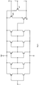
- a data source supplies a driving voltage to input I of the first stage of a cascade of d.c. coupled CMOS inverters.
- Each stage of this cascade is composed of two CMOS transistors, one p-type and one n-type, with gates and drains connected together and with sources connected respectively to the positive power supply terminal Vdd and to ground.
- Vdd positive power supply terminal
- one transistor is saturated while the other one is cut off, so no current flows between Vdd and ground and no power dissipation occurs.
- both transistors can conduct but the phenomenon is very rapid and therefore dissipated power is modest.
- the output of the last stage of this cascade is connected to the gate of a CMOS transistor MS, of the p-type.
- This transistor drain is connected to a terminal L, which can be connected to the anode of an optical source to be driven, for example a laser diode with grounded cathode; the source of MS, instead, is connected to the drain of a transistor MM, whose gate is in turn connected to an external terminal M which receives a voltage controlling the modulation current, and whose source is connected to power supply terminal Vdd.
- Vdd and L there is also a p-type transistor MP, whose gate is connected to the outside terminal P which receives the voltage controlling the bias current.
- the dimensions of the transistors used in the various stages of the cascade of inverters increase as the final stage is approached.
- the parasitic capacities at the input of these inverter stages and the output currents that they can supply or absorb are directly proportional to the surface areas of the transistors utilised. Proceeding from the first to the last stage, therefore, the input capacity of the inverter stage increases, as well as the available output current.
- the charging and discharging time of the input capacity of a driven stage inversely proportional to the switching speed of the input voltage, decreases as the output current respectively supplied or absorbed by the driving stage increases.
- the cascade of inverters having the transistor-dimensioning characteristics described above allows to drive with sufficient speed the input capacity of transistor MS, whose area is relatively large precisely to allow it to provide fast enough current variations on the load.
- the problem of driving in an analogous way the gates of transistors MM and MP, both of which have an area that is comparable to that of MS, need not be addressed, since they are subjected to voltages that remain constant once they have been set at the desired value.
- the number of inverter stages is odd.
- the gate of MS is at high logic level and since the transistor is of the p-type, it is cut off, so that only the bias current supplied by MP can flow toward terminal L; conversely, when the voltage on I is at high logic level, the gate of MS is at low logic level and the transistor is saturated, i.e. it behaves like a switch switched on, and therefore the current that can flow toward terminal L is given by the sum of the bias current and of the modulation current supplied by MM.
- These two currents depend on the voltages to which terminals M and P are subjected.
- both the tension on M and that on P can be adjusted independently from each other, for instance connecting to each terminal the cursor of a multi-turn potentiometer connected between the power supply and ground and varying the positions of these cursors according to the voltages one desires to impose.
- Fig. 2 represents a circuit similar to the one described above, suitable for driving an optical source whose terminals are insulated from the case.
- the signal supplied by an information source, not shown, is supplied to input I of a cascade of inverters, which drives the gate of a n-type CMOS transistor, indicated as MS'.
- This transistor which acts as a switch for the modulation current, is connected through terminal L to the cathode of an optical source.
- a n-type CMOS transistor, indicated as MM' is arranged in series with transistor MS' and its source is grounded while its gate is connected to a terminal M.
- the voltage on M can be adjusted externally, for instance by means of a variable resistor, and on this voltage depends the maximum value of the modulation current.
- a n-type CMOS transistor MP' has its gate connected to a terminal P, its source connected to ground and its drain connected to terminal L. Setting the voltage on terminal P externally, it is possible to control the bias current flowing through the optical source.
- an even number of stages is used in the cascade of inverters: to a high logic level at the input of the cascade of inverters a high logic level corresponds on the gate of MS', which is thus saturated and lets the modulation current supplied by MM' flow to ground. In this operating condition, a current given by the sum of the modulation and bias currents flows in the optical source. Conversely, when at the input of the cascade of inverters there is a low logic level, the gate of MS' is itself at low logic level and that transistor is cut off, to that only the bias current is drained from the optical source.
- Fig. 3 represents the eye diagram related to the schematic diagram in Fig. 1 for a flow of data at 622 Mbit/s, where time (625 ps/division) is reported on the x-coordinates and the signal amplitude (100 mV/division) is reported on the y-coordinates. From this diagram it is evident that noise is limited and inter-symbol error is practically absent. This means that the voltage that determines the value of the bias current and the voltage that determines the value of the modulation current are not influenced by the voltage variations on the gate of the modulation switch transistor even for high bit rates.
Landscapes
- Physics & Mathematics (AREA)
- Condensed Matter Physics & Semiconductors (AREA)
- General Physics & Mathematics (AREA)
- Electromagnetism (AREA)
- Optics & Photonics (AREA)
- Semiconductor Lasers (AREA)
- Optical Communication System (AREA)
Applications Claiming Priority (2)
| Application Number | Priority Date | Filing Date | Title |
|---|---|---|---|
| IT94TO000462A IT1268070B1 (it) | 1994-06-06 | 1994-06-06 | Circuito in tecnologia cmos per il pilotaggo ad alta velocita' di sorgenti ottiche. |
| ITTO940462 | 1994-06-06 |
Publications (3)
| Publication Number | Publication Date |
|---|---|
| EP0687046A2 true EP0687046A2 (de) | 1995-12-13 |
| EP0687046A3 EP0687046A3 (de) | 1996-04-24 |
| EP0687046B1 EP0687046B1 (de) | 1997-05-21 |
Family
ID=11412578
Family Applications (1)
| Application Number | Title | Priority Date | Filing Date |
|---|---|---|---|
| EP95108625A Expired - Lifetime EP0687046B1 (de) | 1994-06-06 | 1995-06-05 | Hochgeschwindigkeitstreiberstufe in CMOS-Technologie für optische Quellen |
Country Status (6)
| Country | Link |
|---|---|
| US (1) | US5589786A (de) |
| EP (1) | EP0687046B1 (de) |
| JP (1) | JP2640443B2 (de) |
| CA (1) | CA2150656C (de) |
| DE (2) | DE687046T1 (de) |
| IT (1) | IT1268070B1 (de) |
Cited By (2)
| Publication number | Priority date | Publication date | Assignee | Title |
|---|---|---|---|---|
| EP0803947A2 (de) * | 1996-04-24 | 1997-10-29 | CSELT Centro Studi e Laboratori Telecomunicazioni S.p.A. | Hochgeschwindigkeitsschaltung in cmos Technologie für optische Quellen |
| US6449297B1 (en) | 1999-10-25 | 2002-09-10 | Kabushiki Kaisha Toshiba | Power supply unit for solid-state laser, solid state laser, and laser beam generator |
Families Citing this family (27)
| Publication number | Priority date | Publication date | Assignee | Title |
|---|---|---|---|---|
| US6246278B1 (en) * | 1995-12-22 | 2001-06-12 | Lsi Logic Corporation | High speed single phase to dual phase clock divider |
| US5978393A (en) * | 1997-08-25 | 1999-11-02 | Digital Optics Corporation | Laser diode power output controller and method thereof |
| US6211659B1 (en) * | 2000-03-14 | 2001-04-03 | Intel Corporation | Cascode circuits in dual-Vt, BICMOS and DTMOS technologies |
| JP2001326569A (ja) * | 2000-05-16 | 2001-11-22 | Toshiba Corp | Led駆動回路及び光送信モジュール |
| US6493275B2 (en) | 2000-08-07 | 2002-12-10 | Matsushita Electric Industrial Co., Ltd. | Semiconductor integrated circuit device and electronic equipment |
| US7173551B2 (en) | 2000-12-21 | 2007-02-06 | Quellan, Inc. | Increasing data throughput in optical fiber transmission systems |
| US6590916B2 (en) * | 2001-02-08 | 2003-07-08 | Quantum Devices, Inc. | Method for fabricating a wave division laser array multiplexer |
| US7149256B2 (en) | 2001-03-29 | 2006-12-12 | Quellan, Inc. | Multilevel pulse position modulation for efficient fiber optic communication |
| US7307569B2 (en) | 2001-03-29 | 2007-12-11 | Quellan, Inc. | Increasing data throughput in optical fiber transmission systems |
| EP1384338B1 (de) | 2001-04-04 | 2010-12-15 | Quellan, Inc. | Verfahren und system zum decodieren von mehrpegelsignalen |
| US7212580B2 (en) | 2002-02-15 | 2007-05-01 | Quellan, Inc. | Multi-level signal clock recovery technique |
| WO2003077423A2 (en) | 2002-03-08 | 2003-09-18 | Quellan, Inc. | High speed analog-to-digital converter using a unique gray code having minimal bit transitions |
| US7035361B2 (en) | 2002-07-15 | 2006-04-25 | Quellan, Inc. | Adaptive noise filtering and equalization for optimal high speed multilevel signal decoding |
| US7934144B2 (en) | 2002-11-12 | 2011-04-26 | Quellan, Inc. | High-speed analog-to-digital conversion with improved robustness to timing uncertainty |
| GB2421674B (en) | 2003-08-07 | 2006-11-15 | Quellan Inc | Method and system for crosstalk cancellation |
| US7804760B2 (en) | 2003-08-07 | 2010-09-28 | Quellan, Inc. | Method and system for signal emulation |
| US7039258B2 (en) * | 2003-08-15 | 2006-05-02 | Luxtera, Inc. | Distributed amplifier optical modulators |
| US7515775B1 (en) * | 2003-08-15 | 2009-04-07 | Luxtera, Inc. | Distributed amplifier optical modulator |
| DE602004030032D1 (de) | 2003-11-17 | 2010-12-23 | Quellan Inc | Verfahren und system zur löschung von antennenstörungen |
| US7616700B2 (en) | 2003-12-22 | 2009-11-10 | Quellan, Inc. | Method and system for slicing a communication signal |
| FR2872630B1 (fr) * | 2004-07-01 | 2006-12-01 | St Microelectronics Sa | Circuit integre tolerant au phenomene de verrouillage |
| US7725079B2 (en) | 2004-12-14 | 2010-05-25 | Quellan, Inc. | Method and system for automatic control in an interference cancellation device |
| US7522883B2 (en) | 2004-12-14 | 2009-04-21 | Quellan, Inc. | Method and system for reducing signal interference |
| US9252983B2 (en) | 2006-04-26 | 2016-02-02 | Intersil Americas LLC | Method and system for reducing radiated emissions from a communications channel |
| US8763877B2 (en) | 2010-09-30 | 2014-07-01 | Ethicon Endo-Surgery, Inc. | Surgical instruments with reconfigurable shaft segments |
| JP6244674B2 (ja) * | 2013-06-04 | 2017-12-13 | 富士通株式会社 | 光通信装置及び光通信装置制御方法 |
| US20200375483A1 (en) * | 2019-05-30 | 2020-12-03 | Welch Allyn, Inc. | Photoplethysmography device with a compensation current source |
Family Cites Families (7)
| Publication number | Priority date | Publication date | Assignee | Title |
|---|---|---|---|---|
| US4412140A (en) * | 1981-11-19 | 1983-10-25 | Motorola, Inc. | Circuit for reducing current to light emitting diode of optically coupled driver |
| US4819241A (en) * | 1985-08-16 | 1989-04-04 | Kabushiki Kaisha Toshiba | Laser diode driving circuit |
| SU1372612A1 (ru) * | 1985-11-29 | 1988-02-07 | Предприятие П/Я М-5912 | Устройство передачи цифровых сигналов с гальваническим разделением |
| IT1201859B (it) * | 1986-12-10 | 1989-02-02 | Sgs Microelettronica Spa | Circuito logico cmos |
| US5111065A (en) * | 1990-03-23 | 1992-05-05 | Massachusetts Institute Of Technology | Diode driver circuit utilizing discrete-value DC current source |
| US5089727A (en) * | 1990-04-02 | 1992-02-18 | Motorola, Inc. | Pulsed driver circuit |
| DE4227097A1 (de) * | 1992-08-17 | 1994-02-24 | Sel Alcatel Ag | Schaltungsanordnung zur Amplitudenmodulation des Ansteuersignals eines Lasers |
-
1994
- 1994-06-06 IT IT94TO000462A patent/IT1268070B1/it active IP Right Grant
-
1995
- 1995-05-31 CA CA002150656A patent/CA2150656C/en not_active Expired - Fee Related
- 1995-06-01 US US08/456,712 patent/US5589786A/en not_active Expired - Fee Related
- 1995-06-05 DE DE0687046T patent/DE687046T1/de active Pending
- 1995-06-05 EP EP95108625A patent/EP0687046B1/de not_active Expired - Lifetime
- 1995-06-05 DE DE69500311T patent/DE69500311T2/de not_active Expired - Fee Related
- 1995-06-06 JP JP7161584A patent/JP2640443B2/ja not_active Expired - Lifetime
Non-Patent Citations (1)
| Title |
|---|
| "Custom Integrated Circuits Conference", 1992, IEEE, article M. STEYAERT ET AL.: "150 Mbit/s CMOS LED-driver and PIN-receiver IC for Optical Communication" |
Cited By (3)
| Publication number | Priority date | Publication date | Assignee | Title |
|---|---|---|---|---|
| EP0803947A2 (de) * | 1996-04-24 | 1997-10-29 | CSELT Centro Studi e Laboratori Telecomunicazioni S.p.A. | Hochgeschwindigkeitsschaltung in cmos Technologie für optische Quellen |
| EP0803947A3 (de) * | 1996-04-24 | 2000-03-22 | CSELT Centro Studi e Laboratori Telecomunicazioni S.p.A. | Hochgeschwindigkeitsschaltung in cmos Technologie für optische Quellen |
| US6449297B1 (en) | 1999-10-25 | 2002-09-10 | Kabushiki Kaisha Toshiba | Power supply unit for solid-state laser, solid state laser, and laser beam generator |
Also Published As
| Publication number | Publication date |
|---|---|
| DE69500311T2 (de) | 1997-10-02 |
| DE687046T1 (de) | 1996-11-28 |
| CA2150656C (en) | 1999-09-14 |
| JPH07335957A (ja) | 1995-12-22 |
| CA2150656A1 (en) | 1995-12-07 |
| EP0687046A3 (de) | 1996-04-24 |
| ITTO940462A0 (it) | 1994-06-06 |
| EP0687046B1 (de) | 1997-05-21 |
| IT1268070B1 (it) | 1997-02-20 |
| JP2640443B2 (ja) | 1997-08-13 |
| US5589786A (en) | 1996-12-31 |
| ITTO940462A1 (it) | 1995-12-06 |
| DE69500311D1 (de) | 1997-06-26 |
Similar Documents
| Publication | Publication Date | Title |
|---|---|---|
| EP0687046B1 (de) | Hochgeschwindigkeitstreiberstufe in CMOS-Technologie für optische Quellen | |
| EP0563580B1 (de) | Steuerschaltung für lichtemittierende Vorrichtung | |
| US7411987B2 (en) | System and method for using an output transformer for laser diode drivers | |
| JP3130571B2 (ja) | 半導体レーザアレイ装置 | |
| CA1229655A (en) | Led driver circuit | |
| US4799224A (en) | Driver for a semiconductor laser | |
| IL133819A (en) | Fast semiconductor laser driving circuits | |
| US8705979B2 (en) | LD driver with an improved falling edge of driving signal and optical transmitter providing the same | |
| NZ200193A (en) | Optical receiver | |
| US20050123013A1 (en) | Laser diode driver circuit and optical communication device | |
| US4339822A (en) | Diode laser digital modulator | |
| EP0110317B1 (de) | Treiberschaltung mit geringem Stromverbrauch für Übertragungsleitungen für Digitalsignale grosser Geschwindigkeit | |
| US5734170A (en) | Driver for light emitting device | |
| US8737442B2 (en) | Driver circuit for laser diode outputting pre-emphasized signal | |
| US6483345B1 (en) | High speed level shift circuit for low voltage output | |
| US6778569B2 (en) | Optical source driver with improved input stage | |
| EP0577896A1 (de) | Vorverstärker | |
| KR20090098746A (ko) | 구동 회로, 구동 회로의 작동 방법, 및 구동 회로의 전류 미러의 사용 방법 | |
| US6516015B1 (en) | Laser driver and optical transceiver | |
| CA2203489C (en) | Circuit in cmos technology for high speed driving of optical sources | |
| US7006543B2 (en) | System and circuit for a multi-channel optoelectronic device driver | |
| JP3092630B2 (ja) | 制御回路及びその制御回路により制御される集積回路 | |
| US4633525A (en) | Light-emitting diode device for suppressing thermal time-constant effects | |
| JP3482165B2 (ja) | レーザー駆動回路および光送受信装置 | |
| US6680468B1 (en) | Electrical-supply-free MOS integrated circuit |
Legal Events
| Date | Code | Title | Description |
|---|---|---|---|
| PUAI | Public reference made under article 153(3) epc to a published international application that has entered the european phase |
Free format text: ORIGINAL CODE: 0009012 |
|
| AK | Designated contracting states |
Kind code of ref document: A2 Designated state(s): DE FR GB IT NL SE |
|
| PUAL | Search report despatched |
Free format text: ORIGINAL CODE: 0009013 |
|
| AK | Designated contracting states |
Kind code of ref document: A3 Designated state(s): DE FR GB IT NL SE |
|
| EL | Fr: translation of claims filed | ||
| 17P | Request for examination filed |
Effective date: 19960531 |
|
| TCNL | Nl: translation of patent claims filed | ||
| DET | De: translation of patent claims | ||
| GRAG | Despatch of communication of intention to grant |
Free format text: ORIGINAL CODE: EPIDOS AGRA |
|
| 17Q | First examination report despatched |
Effective date: 19970122 |
|
| GRAH | Despatch of communication of intention to grant a patent |
Free format text: ORIGINAL CODE: EPIDOS IGRA |
|
| GRAH | Despatch of communication of intention to grant a patent |
Free format text: ORIGINAL CODE: EPIDOS IGRA |
|
| GRAA | (expected) grant |
Free format text: ORIGINAL CODE: 0009210 |
|
| AK | Designated contracting states |
Kind code of ref document: B1 Designated state(s): DE FR GB IT NL SE |
|
| REF | Corresponds to: |
Ref document number: 69500311 Country of ref document: DE Date of ref document: 19970626 |
|
| ET | Fr: translation filed | ||
| PLBE | No opposition filed within time limit |
Free format text: ORIGINAL CODE: 0009261 |
|
| STAA | Information on the status of an ep patent application or granted ep patent |
Free format text: STATUS: NO OPPOSITION FILED WITHIN TIME LIMIT |
|
| 26N | No opposition filed | ||
| PGFP | Annual fee paid to national office [announced via postgrant information from national office to epo] |
Ref country code: SE Payment date: 19990525 Year of fee payment: 5 |
|
| PGFP | Annual fee paid to national office [announced via postgrant information from national office to epo] |
Ref country code: GB Payment date: 19990602 Year of fee payment: 5 |
|
| PGFP | Annual fee paid to national office [announced via postgrant information from national office to epo] |
Ref country code: DE Payment date: 19990617 Year of fee payment: 5 |
|
| PGFP | Annual fee paid to national office [announced via postgrant information from national office to epo] |
Ref country code: FR Payment date: 19990628 Year of fee payment: 5 |
|
| PGFP | Annual fee paid to national office [announced via postgrant information from national office to epo] |
Ref country code: NL Payment date: 19990630 Year of fee payment: 5 |
|
| PG25 | Lapsed in a contracting state [announced via postgrant information from national office to epo] |
Ref country code: GB Free format text: LAPSE BECAUSE OF NON-PAYMENT OF DUE FEES Effective date: 20000605 |
|
| PG25 | Lapsed in a contracting state [announced via postgrant information from national office to epo] |
Ref country code: SE Free format text: LAPSE BECAUSE OF NON-PAYMENT OF DUE FEES Effective date: 20000606 |
|
| PG25 | Lapsed in a contracting state [announced via postgrant information from national office to epo] |
Ref country code: NL Free format text: LAPSE BECAUSE OF NON-PAYMENT OF DUE FEES Effective date: 20010101 |
|
| GBPC | Gb: european patent ceased through non-payment of renewal fee |
Effective date: 20000605 |
|
| EUG | Se: european patent has lapsed |
Ref document number: 95108625.5 |
|
| PG25 | Lapsed in a contracting state [announced via postgrant information from national office to epo] |
Ref country code: FR Free format text: LAPSE BECAUSE OF NON-PAYMENT OF DUE FEES Effective date: 20010228 |
|
| NLV4 | Nl: lapsed or anulled due to non-payment of the annual fee |
Effective date: 20010101 |
|
| REG | Reference to a national code |
Ref country code: FR Ref legal event code: ST |
|
| PG25 | Lapsed in a contracting state [announced via postgrant information from national office to epo] |
Ref country code: DE Free format text: LAPSE BECAUSE OF NON-PAYMENT OF DUE FEES Effective date: 20010403 |
|
| PGFP | Annual fee paid to national office [announced via postgrant information from national office to epo] |
Ref country code: IT Payment date: 20140625 Year of fee payment: 20 |