EP0676484A2 - Transparent diamond films and method for making - Google Patents
Transparent diamond films and method for making Download PDFInfo
- Publication number
- EP0676484A2 EP0676484A2 EP95201231A EP95201231A EP0676484A2 EP 0676484 A2 EP0676484 A2 EP 0676484A2 EP 95201231 A EP95201231 A EP 95201231A EP 95201231 A EP95201231 A EP 95201231A EP 0676484 A2 EP0676484 A2 EP 0676484A2
- Authority
- EP
- European Patent Office
- Prior art keywords
- diamond
- hydrogen
- diamond film
- film
- substrate
- Prior art date
- Legal status (The legal status is an assumption and is not a legal conclusion. Google has not performed a legal analysis and makes no representation as to the accuracy of the status listed.)
- Granted
Links
Images


Classifications
-
- C—CHEMISTRY; METALLURGY
- C23—COATING METALLIC MATERIAL; COATING MATERIAL WITH METALLIC MATERIAL; CHEMICAL SURFACE TREATMENT; DIFFUSION TREATMENT OF METALLIC MATERIAL; COATING BY VACUUM EVAPORATION, BY SPUTTERING, BY ION IMPLANTATION OR BY CHEMICAL VAPOUR DEPOSITION, IN GENERAL; INHIBITING CORROSION OF METALLIC MATERIAL OR INCRUSTATION IN GENERAL
- C23C—COATING METALLIC MATERIAL; COATING MATERIAL WITH METALLIC MATERIAL; SURFACE TREATMENT OF METALLIC MATERIAL BY DIFFUSION INTO THE SURFACE, BY CHEMICAL CONVERSION OR SUBSTITUTION; COATING BY VACUUM EVAPORATION, BY SPUTTERING, BY ION IMPLANTATION OR BY CHEMICAL VAPOUR DEPOSITION, IN GENERAL
- C23C16/00—Chemical coating by decomposition of gaseous compounds, without leaving reaction products of surface material in the coating, i.e. chemical vapour deposition [CVD] processes
- C23C16/22—Chemical coating by decomposition of gaseous compounds, without leaving reaction products of surface material in the coating, i.e. chemical vapour deposition [CVD] processes characterised by the deposition of inorganic material, other than metallic material
- C23C16/26—Deposition of carbon only
- C23C16/27—Diamond only
- C23C16/271—Diamond only using hot filaments
-
- C—CHEMISTRY; METALLURGY
- C01—INORGANIC CHEMISTRY
- C01B—NON-METALLIC ELEMENTS; COMPOUNDS THEREOF; METALLOIDS OR COMPOUNDS THEREOF NOT COVERED BY SUBCLASS C01C
- C01B32/00—Carbon; Compounds thereof
- C01B32/25—Diamond
-
- C—CHEMISTRY; METALLURGY
- C23—COATING METALLIC MATERIAL; COATING MATERIAL WITH METALLIC MATERIAL; CHEMICAL SURFACE TREATMENT; DIFFUSION TREATMENT OF METALLIC MATERIAL; COATING BY VACUUM EVAPORATION, BY SPUTTERING, BY ION IMPLANTATION OR BY CHEMICAL VAPOUR DEPOSITION, IN GENERAL; INHIBITING CORROSION OF METALLIC MATERIAL OR INCRUSTATION IN GENERAL
- C23C—COATING METALLIC MATERIAL; COATING MATERIAL WITH METALLIC MATERIAL; SURFACE TREATMENT OF METALLIC MATERIAL BY DIFFUSION INTO THE SURFACE, BY CHEMICAL CONVERSION OR SUBSTITUTION; COATING BY VACUUM EVAPORATION, BY SPUTTERING, BY ION IMPLANTATION OR BY CHEMICAL VAPOUR DEPOSITION, IN GENERAL
- C23C16/00—Chemical coating by decomposition of gaseous compounds, without leaving reaction products of surface material in the coating, i.e. chemical vapour deposition [CVD] processes
- C23C16/01—Chemical coating by decomposition of gaseous compounds, without leaving reaction products of surface material in the coating, i.e. chemical vapour deposition [CVD] processes on temporary substrates, e.g. substrates subsequently removed by etching
-
- C—CHEMISTRY; METALLURGY
- C23—COATING METALLIC MATERIAL; COATING MATERIAL WITH METALLIC MATERIAL; CHEMICAL SURFACE TREATMENT; DIFFUSION TREATMENT OF METALLIC MATERIAL; COATING BY VACUUM EVAPORATION, BY SPUTTERING, BY ION IMPLANTATION OR BY CHEMICAL VAPOUR DEPOSITION, IN GENERAL; INHIBITING CORROSION OF METALLIC MATERIAL OR INCRUSTATION IN GENERAL
- C23C—COATING METALLIC MATERIAL; COATING MATERIAL WITH METALLIC MATERIAL; SURFACE TREATMENT OF METALLIC MATERIAL BY DIFFUSION INTO THE SURFACE, BY CHEMICAL CONVERSION OR SUBSTITUTION; COATING BY VACUUM EVAPORATION, BY SPUTTERING, BY ION IMPLANTATION OR BY CHEMICAL VAPOUR DEPOSITION, IN GENERAL
- C23C16/00—Chemical coating by decomposition of gaseous compounds, without leaving reaction products of surface material in the coating, i.e. chemical vapour deposition [CVD] processes
- C23C16/22—Chemical coating by decomposition of gaseous compounds, without leaving reaction products of surface material in the coating, i.e. chemical vapour deposition [CVD] processes characterised by the deposition of inorganic material, other than metallic material
- C23C16/26—Deposition of carbon only
- C23C16/27—Diamond only
- C23C16/279—Diamond only control of diamond crystallography
-
- Y—GENERAL TAGGING OF NEW TECHNOLOGICAL DEVELOPMENTS; GENERAL TAGGING OF CROSS-SECTIONAL TECHNOLOGIES SPANNING OVER SEVERAL SECTIONS OF THE IPC; TECHNICAL SUBJECTS COVERED BY FORMER USPC CROSS-REFERENCE ART COLLECTIONS [XRACs] AND DIGESTS
- Y10—TECHNICAL SUBJECTS COVERED BY FORMER USPC
- Y10S—TECHNICAL SUBJECTS COVERED BY FORMER USPC CROSS-REFERENCE ART COLLECTIONS [XRACs] AND DIGESTS
- Y10S428/00—Stock material or miscellaneous articles
- Y10S428/922—Static electricity metal bleed-off metallic stock
- Y10S428/9335—Product by special process
- Y10S428/938—Vapor deposition or gas diffusion
Definitions
- the present invention relates to vapor deposited transparent polycrystalline diamond films. More particularly, the present invention relates the method of introducing a particular mixture of hydrogen and methane into a heated reaction zone adjacent to a substrate such as molybdenum, to effect polycrystalline diamond film deposition.
- thermoforming materials in the form of free-standing polycrystalline transparent diamond films having thicknesses of from 50 to 5000 microns with lateral dimensions exceeding 10 millimeters.
- the present invention is based on the discovery that vapor deposited transparent polycrystalline diamond film can be made at thicknesses greater than 50 microns by passing a particular hydrogen-methane mixture through a filament heated reaction zone adjacent to a suitable substrate, such as a molybdenum substrate, where the hydrogen-methane mixture introduced into the reaction zone has from about 1.5 to about 2 volume percent of methane, based on the total volume of hydrogen and methane.
- a transparent non-adherent polycrystalline diamond film having an optical absorbance of 2.1 cm ⁇ 1 to 32 cm ⁇ 1 can be formed at a growth rate of about 0.4 to 1.0 microns per hour. Thicknesses of at least 50 microns, and as high as 5000 microns or more, can be made having lateral dimensions exceeding 25 centimeters.
- a continuous free-standing, substantially transparent, polycrystalline diamond film having a thickness of at least 50 microns comprising (A) substantially vertical columnar diamond crystals having an average diameter of from about 20 to about 200 microns and a ⁇ 110 ⁇ orientation perpendicular to the base and up to 10,000 parts per million of chemically combined hydrogen which is sufficient to substantially saturate dangling carbon bonds at diamond crystal grain boundaries, carbon dislocations, and carbon vacancies and (B) diamond crystal grain boundaries separating the columnar diamond crystals of (A) where the diamond crystal grain boundaries have a 70°-90° orientation to the diamond crystal base.
- a method of growing a non-adherent substantially transparent polycrystalline diamond film on a substrate which comprises, passing a hydrogen-methane mixture through a heated reaction zone at a temperature of about 600° to about 1000°C and at a pressure from about 3 to about 24 torr which is sufficient to generate active carbon-hydrogen species in the heated reaction zone maintained at a distance of from about 0.3 to about 1 centimeter from the surface of the substrate, where the hydrogen-methane mixture introduced into the heated reaction zone has from 1.5 to about 2 volume percent of methane, based on the total volume of hydrogen and methane.
- Figure 1 shows a quartz bell jar having a metal flange which rests on a base. Inside the quartz bell jar, there is shown a support structure for a filament and several adjacent substrate sections.
- a quartz bell jar at 10 which can be 20"-30" tall and about 4"-6" wide having a metal collar at its base at 11 and a gas inlet at the top at 12.
- the metal collar portion rests on a rubber seal at 13 which can be Neoprene rubber.
- the rubber seal is supported by a metal base, such as steel base structure at 14 which has a vacuum opening at 15.
- the filament is secured by a screw at 21 to a metal plug at 22 which passes through a quartz insulating collar at 23 which is supported by an extension at 24. Electrical contacts are shown from the plug at 25 to a stud at 26 which is insulated from the metal base at 27.
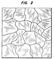
- Figure 2 showing a top view through an optical microscope of 10 to 200 micron columnar diamond crystals of the polycrystalline diamond film of the present invention separated by atomic grain boundaries such as shown at 30.
- FIG. 3 and Figure 3A A further reference to the polycrystalline diamond film of the present invention is shown by Figure 3 and Figure 3A.
- a side view of the polycrystalline diamond film in cross Section, and a detail at 3A further illustrates the substantially transparent columns of diamond crystals having a ⁇ 110 ⁇ orientation perpendicular to the base. Grain boundaries between adjacent diamond crystals having hydrogen atoms saturating dangling carbon bonds are shown at 40 and in detail at 41, where at least 50% of the carbon atoms are believed to be tetrahedrally bonded based on Raman spectroscopy, infrared and X-ray analysis.
- the above mechanism is one possible explanation as to how the transparent diamond film grows on the substrate.
- polycrystalline diamond films made in accordance with the practice of the present invention can be used in a variety of glazing applications as well as heat sinks or semiconductors.
- the tungsten filament was maintained at a temperature between about 2020 to 2040 .
- a separation of about 7-8 millimeters was maintained between the filament and the molybdenum substrate during the deposition which lasted approximately 30 days.
- the substrate temperature was estimated at about 800 . C during the deposition period.
- Transparent polycrystalline diamond films having thicknesses of about 500 microns and lateral dimensions equivalent to the substrates separated from the substrate during the cooling period.
- the diamond films were found to be of good crystalline quality as shown by Raman spectra having an intense peak at 1332 cm ⁇ 1.
- the diamond films were also found to have the characteristic two phonon adsorption of material diamond in the range of 1600-2650 cm ⁇ 1 by infrared spectroscopy.
Abstract
Description
- The present invention relates to vapor deposited transparent polycrystalline diamond films. More particularly, the present invention relates the method of introducing a particular mixture of hydrogen and methane into a heated reaction zone adjacent to a substrate such as molybdenum, to effect polycrystalline diamond film deposition.
- As taught by Spear, Diamond-Ceramic Coating Of The Future, Journal of American Ceramics Society, 72[2]171-91 (1989), the growth of single-crystal films of diamond is critical to many electronic and optical applications, but it is a feat that has not been achieved except for homoepitaxial growth on diamond substrates. There is reported by Peter K. Backmann, et al in the May 15, 1989, edition of Chemical and Engineering News, on page 38, that vapor deposited diamond heat sinks have been developed using plasma jet deposition to produce polycrystalline material up to 4 x 6 x 1 millimeter.
- In Japanese patent 85,141,697, it is reported that free-standing diamond films have been found useful as diaphragms for speakers. S. Kawachi et al, Japanese patent 85(60)-127,292, reports that 10 micron diamond films have been deposited on a graphite substrate. K. Fujii, et al, Japanese patent 85(60)-186,500 teaches that a 6.5 micron thick transparent film can be produced on a substrate using a methane- hydrogen mixture.
- Although various procedures have been developed to make vapor deposited polycrystalline diamond film, it would be desirable to provide glazing materials in the form of free-standing polycrystalline transparent diamond films having thicknesses of from 50 to 5000 microns with lateral dimensions exceeding 10 millimeters.
- The present invention is based on the discovery that vapor deposited transparent polycrystalline diamond film can be made at thicknesses greater than 50 microns by passing a particular hydrogen-methane mixture through a filament heated reaction zone adjacent to a suitable substrate, such as a molybdenum substrate, where the hydrogen-methane mixture introduced into the reaction zone has from about 1.5 to about 2 volume percent of methane, based on the total volume of hydrogen and methane. Surprisingly, a transparent non-adherent polycrystalline diamond film having an optical absorbance of 2.1 cm⁻¹ to 32 cm⁻¹ can be formed at a growth rate of about 0.4 to 1.0 microns per hour. Thicknesses of at least 50 microns, and as high as 5000 microns or more, can be made having lateral dimensions exceeding 25 centimeters.
- There is provided by the present invention, a continuous free-standing, substantially transparent, polycrystalline diamond film having a thickness of at least 50 microns comprising (A) substantially vertical columnar diamond crystals having an average diameter of from about 20 to about 200 microns and a 〈110〉 orientation perpendicular to the base and up to 10,000 parts per million of chemically combined hydrogen which is sufficient to substantially saturate dangling carbon bonds at diamond crystal grain boundaries, carbon dislocations, and carbon vacancies and (B) diamond crystal grain boundaries separating the columnar diamond crystals of (A) where the diamond crystal grain boundaries have a 70°-90° orientation to the diamond crystal base.
- In another aspect of the present invention, there is provided a method of growing a non-adherent substantially transparent polycrystalline diamond film on a substrate which comprises, passing a hydrogen-methane mixture through a heated reaction zone at a temperature of about 600° to about 1000°C and at a pressure from about 3 to about 24 torr which is sufficient to generate active carbon-hydrogen species in the heated reaction zone maintained at a distance of from about 0.3 to about 1 centimeter from the surface of the substrate, where the hydrogen-methane mixture introduced into the heated reaction zone has from 1.5 to about 2 volume percent of methane, based on the total volume of hydrogen and methane.
- A typical apparatus which can be used to form the transparent polycrystalline diamond film of the present invention is shown by Figure 1. Figure 1 shows a quartz bell jar having a metal flange which rests on a base. Inside the quartz bell jar, there is shown a support structure for a filament and several adjacent substrate sections.
- More particularly, there is shown a quartz bell jar at 10 which can be 20"-30" tall and about 4"-6" wide having a metal collar at its base at 11 and a gas inlet at the top at 12. The metal collar portion rests on a rubber seal at 13 which can be Neoprene rubber. The rubber seal is supported by a metal base, such as steel base structure at 14 which has a vacuum opening at 15.
- Inside the quartz bell jar there is shown a supporting stand at 16 for an extension at 17 for holding several substrate structures, such as molybdenum at 18 and 19 and a filament at 20. The filament is secured by a screw at 21 to a metal plug at 22 which passes through a quartz insulating collar at 23 which is supported by an extension at 24. Electrical contacts are shown from the plug at 25 to a stud at 26 which is insulated from the metal base at 27.
- Reference also is made to Figure 2, showing a top view through an optical microscope of 10 to 200 micron columnar diamond crystals of the polycrystalline diamond film of the present invention separated by atomic grain boundaries such as shown at 30.
- A further reference to the polycrystalline diamond film of the present invention is shown by Figure 3 and Figure 3A. A side view of the polycrystalline diamond film in cross Section, and a detail at 3A further illustrates the substantially transparent columns of diamond crystals having a 〈110〉 orientation perpendicular to the base. Grain boundaries between adjacent diamond crystals having hydrogen atoms saturating dangling carbon bonds are shown at 40 and in detail at 41, where at least 50% of the carbon atoms are believed to be tetrahedrally bonded based on Raman spectroscopy, infrared and X-ray analysis.
- A detailed discussion of Miller Indices describing crystal planes of atoms differentiating between 〈010〉, 〈110〉 and 〈111〉 orientation is shown on pages 65-69 in Elements of Material Science, Second Edition, 1964, by Lawrence H. VanVlack of Addison-Wisley Publishing Company, Reading, Massachusetts which is incorporated herein by reference.
- A detailed discussion on chemical bonding and structure discussing the hybridization theory and molecular geometry with respect to tetrahedral bonding of carbon atoms with hydrogen is shown by Ernest Griswold, Chemical Bonding and Structure, pages 55-102, 1968, Raytheon Education Company, which is incorporated herein by reference.
- The following shows that dissociation of hydrogen and methane on a heated tungsten filament in accordance with the practice of the method of the present invention.

- The above mechanism is one possible explanation as to how the transparent diamond film grows on the substrate.
- As described by Ch. Wild et al. in the First Proceedings For International ECS Symposium on Diamond and Diamond-Like Films, Los Angeles, May 7-12, 1989 for "Optical and Structural Characterization of CVD Diamond", which is incorporated herein by reference, infrared and Raman spectroscopy as well as X-ray diffraction have been used to investigate polycrystalline diamond films prepared by the method of the present invention. The absorption spectrum of a 400 micron thick free-standing diamond wafer established that the film had a hydrogen concentration of about 5000 part per million. Raman spectroscopy was used to establish that the observed polycrystalline film was significantly different from graphite, since it contained a significant level of tetrahydral carbon atoms. X-ray diffraction measurements revealed that the polycrystalline film made in accordance with the practice of the present invention had a preferential alignment of the 〈110〉 planes perpendicular to the growth direction and indicated that the diamond crystal grain boundaries had a 70.-90. orientation to the base.
- The polycrystalline diamond films made in accordance with the practice of the present invention can be used in a variety of glazing applications as well as heat sinks or semiconductors.
- In order that those skilled in the art will be better able to practice the present invention, the following example is given by way of illustration and not by way of limitation.
- A mixture of 1.75 volume % of methane and 98.25 volume % of hydrogen, measured under atmospheric conditions, was introduced into a reaction vessel as shown by Figure 1. A gas flow rate of about 400 cubic centimeters per minute was maintained. There was used two 1 1/4" x 1/4" x 9" molybdenum substrates and a 9 1/2" #218 tungsten filament having a diameter of .030". The tungsten filament was maintained at a temperature between about 2020 to 2040.C. A separation of about 7-8 millimeters was maintained between the filament and the molybdenum substrate during the deposition which lasted approximately 30 days. The substrate temperature was estimated at about 800.C during the deposition period.
- At the termination of the 30 day deposition period, the apparatus was allowed to cool to room temperature. Transparent polycrystalline diamond films having thicknesses of about 500 microns and lateral dimensions equivalent to the substrates separated from the substrate during the cooling period.
- The diamond films were found to be of good crystalline quality as shown by Raman spectra having an intense peak at 1332 cm⁻¹. The diamond films were also found to have the characteristic two phonon adsorption of material diamond in the range of 1600-2650 cm⁻¹ by infrared spectroscopy.
- Although the above example is directed to only a few of the very many variables which can be used in the practice of the method of the present invention to make the polycrystalline diamond films, it should be understood that a much broader variety of conditions, apparatus arrangements and materials can be used as set forth in the description preceding this example.
Claims (7)
- A transparent or substantially transparent polycrystalline diamond film having a thickness of at least about 50 microns.
- A transparent or substantially transparent diamond film in accordance with Claim 1, wherein the diamond film has a thickness between about 200 microns and about 500 microns.
- A transparent or substantially transparent diamond film in accordance with Claim 1 or Claim 2 wherein the diamond film comprises substantially vertical columnar diamond crystals having a preferred [110] orientation perpendicular to the base of the film.
- A substantially transparent diamond film in accordance with any preceding claim having up to 10,000 ppm of chemically combined hydrogen.
- A substantially transparent diamond film in accordance with any preceding claim, having diamond grain boundaries separating the columnar diamond crystals where said boundaries have between a 70⁰ to a 90⁰ orientation to the base of the film.
- A method of growing a non-adherent substantially transparent polycrystalline diamond film on a substrate which comprises passing a hydrogen-methane mixture through a heated zone at a temperature of about 600⁰C to about 1000⁰C at a pressure of about 3 to about 24 torr which is sufficient to generate active carbon-hydrogen species in the heated zone maintained at a distance of from about 0.3 to about 1 centimeter on the surface of the substrate, where the hydrogen-methane mixture introduced into the heated zone has from about 1.5 to about 2 volume% of methane based on the total volume of hydrogen and methane.
- A method in accordance with Claim 6, where the substrate is a molybdenum substrate.
Applications Claiming Priority (3)
| Application Number | Priority Date | Filing Date | Title |
|---|---|---|---|
| US407179 | 1989-09-14 | ||
| US07/407,179 US5110579A (en) | 1989-09-14 | 1989-09-14 | Transparent diamond films and method for making |
| EP90116058A EP0417512B1 (en) | 1989-09-14 | 1990-08-22 | Transparent diamond films and method for making |
Related Parent Applications (1)
| Application Number | Title | Priority Date | Filing Date |
|---|---|---|---|
| EP90116058A Division EP0417512B1 (en) | 1989-09-14 | 1990-08-22 | Transparent diamond films and method for making |
Publications (3)
| Publication Number | Publication Date |
|---|---|
| EP0676484A2 true EP0676484A2 (en) | 1995-10-11 |
| EP0676484A3 EP0676484A3 (en) | 1995-12-06 |
| EP0676484B1 EP0676484B1 (en) | 1999-03-24 |
Family
ID=23610962
Family Applications (2)
| Application Number | Title | Priority Date | Filing Date |
|---|---|---|---|
| EP90116058A Revoked EP0417512B1 (en) | 1989-09-14 | 1990-08-22 | Transparent diamond films and method for making |
| EP95201231A Revoked EP0676484B1 (en) | 1989-09-14 | 1990-08-22 | Transparent diamond films and method for making |
Family Applications Before (1)
| Application Number | Title | Priority Date | Filing Date |
|---|---|---|---|
| EP90116058A Revoked EP0417512B1 (en) | 1989-09-14 | 1990-08-22 | Transparent diamond films and method for making |
Country Status (8)
| Country | Link |
|---|---|
| US (1) | US5110579A (en) |
| EP (2) | EP0417512B1 (en) |
| JP (2) | JP3176614B2 (en) |
| KR (2) | KR970005187B1 (en) |
| AT (2) | ATE178102T1 (en) |
| CA (1) | CA2021113A1 (en) |
| DE (2) | DE69023847T2 (en) |
| IE (1) | IE73671B1 (en) |
Cited By (3)
| Publication number | Priority date | Publication date | Assignee | Title |
|---|---|---|---|---|
| WO1999001589A1 (en) * | 1997-07-01 | 1999-01-14 | E.I. Du Pont De Nemours And Company | Colorless diamond-like carbon coatings |
| GB2397826A (en) * | 2002-12-18 | 2004-08-04 | Bosch Gmbh Robert | Tribologically stressed structural element coated with diamond-like carbon and gas engine or internal combustion engine provided therewith |
| US8114505B2 (en) | 2003-12-05 | 2012-02-14 | Morgan Advanced Ceramics, Inc. | Free-standing silicon carbide articles formed by chemical vapor deposition and methods for their manufacture |
Families Citing this family (37)
| Publication number | Priority date | Publication date | Assignee | Title |
|---|---|---|---|---|
| US6413589B1 (en) | 1988-11-29 | 2002-07-02 | Chou H. Li | Ceramic coating method |
| US5273731A (en) * | 1989-09-14 | 1993-12-28 | General Electric Company | Substantially transparent free standing diamond films |
| KR930011413B1 (en) | 1990-09-25 | 1993-12-06 | 가부시키가이샤 한도오따이 에네루기 겐큐쇼 | Plasma cvd method for using pulsed waveform |
| US5902640A (en) * | 1991-11-25 | 1999-05-11 | The University Of Chicago | Method of improving field emission characteristics of diamond thin films |
| US5286524A (en) * | 1991-12-13 | 1994-02-15 | General Electric Company | Method for producing CVD diamond film substantially free of thermal stress-induced cracks |
| US5443032A (en) * | 1992-06-08 | 1995-08-22 | Air Products And Chemicals, Inc. | Method for the manufacture of large single crystals |
| GB9214479D0 (en) * | 1992-07-08 | 1992-08-19 | Atomic Energy Authority Uk | Pressure transducers |
| US5377522A (en) * | 1993-10-27 | 1995-01-03 | General Electric Company | Diamond wire die with positioned opening |
| US5361621A (en) * | 1993-10-27 | 1994-11-08 | General Electric Company | Multiple grained diamond wire die |
| US5465603A (en) * | 1993-11-05 | 1995-11-14 | General Electric Company | Optically improved diamond wire die |
| US5514242A (en) * | 1993-12-30 | 1996-05-07 | Saint Gobain/Norton Industrial Ceramics Corporation | Method of forming a heat-sinked electronic component |
| EP0668371A1 (en) * | 1994-02-16 | 1995-08-23 | General Electric Company | Semi-transparent diamond film |
| EP0668372A1 (en) * | 1994-02-16 | 1995-08-23 | General Electric Company | Semi-transparent diamond film |
| EP0678592A1 (en) * | 1994-04-20 | 1995-10-25 | General Electric Company | Improved CVD diamond |
| US5507987A (en) * | 1994-04-28 | 1996-04-16 | Saint Gobain/Norton Industrial Ceramics Corp. | Method of making a free-standing diamond film with reduced bowing |
| US5811631A (en) * | 1994-04-29 | 1998-09-22 | Motorola, Inc. | Apparatus and method for decomposition of chemical compounds using a self-supporting member |
| US5672395A (en) * | 1994-05-05 | 1997-09-30 | General Electric Company | Method for enhancing the toughness of CVD diamond |
| US5451430A (en) * | 1994-05-05 | 1995-09-19 | General Electric Company | Method for enhancing the toughness of CVD diamond |
| US5551277A (en) * | 1994-09-23 | 1996-09-03 | General Electric Company | Annular diamond bodies |
| US5634369A (en) * | 1995-07-07 | 1997-06-03 | General Electric Company | Composite diamond wire die |
| US5636545A (en) * | 1995-07-07 | 1997-06-10 | General Electric Company | Composite diamond wire die |
| US5634370A (en) * | 1995-07-07 | 1997-06-03 | General Electric Company | Composite diamond wire die |
| US5620745A (en) * | 1995-12-19 | 1997-04-15 | Saint Gobain/Norton Industrial Ceramics Corp. | Method for coating a substrate with diamond film |
| US6143412A (en) * | 1997-02-10 | 2000-11-07 | President And Fellows Of Harvard College | Fabrication of carbon microstructures |
| US5937514A (en) | 1997-02-25 | 1999-08-17 | Li; Chou H. | Method of making a heat-resistant system |
| US6286206B1 (en) | 1997-02-25 | 2001-09-11 | Chou H. Li | Heat-resistant electronic systems and circuit boards |
| US6582513B1 (en) * | 1998-05-15 | 2003-06-24 | Apollo Diamond, Inc. | System and method for producing synthetic diamond |
| US8591856B2 (en) * | 1998-05-15 | 2013-11-26 | SCIO Diamond Technology Corporation | Single crystal diamond electrochemical electrode |
| US6858080B2 (en) * | 1998-05-15 | 2005-02-22 | Apollo Diamond, Inc. | Tunable CVD diamond structures |
| US6458017B1 (en) | 1998-12-15 | 2002-10-01 | Chou H. Li | Planarizing method |
| US6976904B2 (en) * | 1998-07-09 | 2005-12-20 | Li Family Holdings, Ltd. | Chemical mechanical polishing slurry |
| US6676492B2 (en) | 1998-12-15 | 2004-01-13 | Chou H. Li | Chemical mechanical polishing |
| AU2001281404B2 (en) | 2001-08-08 | 2008-07-03 | Apollo Diamond, Inc. | System and method for producing synthetic diamond |
| US20050123713A1 (en) | 2003-12-05 | 2005-06-09 | Forrest David T. | Articles formed by chemical vapor deposition and methods for their manufacture |
| US7469569B2 (en) * | 2003-12-10 | 2008-12-30 | Diamond Innovations, Inc. | Wire drawing die and method of making |
| US20050181210A1 (en) * | 2004-02-13 | 2005-08-18 | Doering Patrick J. | Diamond structure separation |
| JP6133647B2 (en) * | 2013-03-25 | 2017-05-24 | シチズン時計株式会社 | Electronic equipment with orientation measurement function |
Citations (3)
| Publication number | Priority date | Publication date | Assignee | Title |
|---|---|---|---|---|
| EP0254560A1 (en) * | 1986-07-23 | 1988-01-27 | Sumitomo Electric Industries Limited | Gaseous phase synthesized diamond and method for synthesizing same |
| EP0286306A1 (en) * | 1987-04-03 | 1988-10-12 | Fujitsu Limited | Method and apparatus for vapor deposition of diamond |
| JPS63307196A (en) * | 1987-06-05 | 1988-12-14 | Kobe Steel Ltd | Diamond multilayered thin film and its production |
Family Cites Families (18)
| Publication number | Priority date | Publication date | Assignee | Title |
|---|---|---|---|---|
| US3030187A (en) * | 1958-07-23 | 1962-04-17 | Union Carbide Corp | Synthesis of diamond |
| US3630679A (en) * | 1968-06-26 | 1971-12-28 | Univ Case Western Reserve | Diamond growth process |
| JPS5927754B2 (en) * | 1981-12-17 | 1984-07-07 | 科学技術庁無機材質研究所長 | Diamond synthesis method |
| JPS58135117A (en) * | 1982-01-29 | 1983-08-11 | Natl Inst For Res In Inorg Mater | Preparation of diamond |
| JPS5918197A (en) * | 1982-07-19 | 1984-01-30 | Sumitomo Electric Ind Ltd | Gaseous phase synthesis of diamond |
| JPS60112699A (en) * | 1983-11-24 | 1985-06-19 | Nec Corp | Manufacture of diamond |
| JPS60118694A (en) * | 1983-11-29 | 1985-06-26 | Mitsubishi Metal Corp | Method for synthesizing diamond under low pressure |
| JPS60127292A (en) * | 1983-12-15 | 1985-07-06 | Asahi Chem Ind Co Ltd | Production of diamond |
| JPS60141697A (en) * | 1983-12-27 | 1985-07-26 | Pioneer Electronic Corp | Manufacture of diamond diaphragm |
| JPS60186500A (en) * | 1984-03-06 | 1985-09-21 | Nec Corp | Method for synthesizing diamond from vapor phase |
| US4816286A (en) * | 1985-11-25 | 1989-03-28 | Showa Denko Kabushiki Kaisha | Process for synthesis of diamond by CVD |
| JPS63107898A (en) * | 1986-10-23 | 1988-05-12 | Natl Inst For Res In Inorg Mater | Method for synthesizing diamond with plasma |
| JPS63153815A (en) * | 1986-12-17 | 1988-06-27 | Fujitsu Ltd | Method for vapor phase synthesis of diamond |
| JPS63201601A (en) * | 1987-02-18 | 1988-08-19 | Res Dev Corp Of Japan | Optical window material and its production |
| US4830702A (en) * | 1987-07-02 | 1989-05-16 | General Electric Company | Hollow cathode plasma assisted apparatus and method of diamond synthesis |
| US4925701A (en) * | 1988-05-27 | 1990-05-15 | Xerox Corporation | Processes for the preparation of polycrystalline diamond films |
| US4958592A (en) * | 1988-08-22 | 1990-09-25 | General Electric Company | Resistance heater for diamond production by CVD |
| US4970986A (en) * | 1989-08-03 | 1990-11-20 | General Electric Company | Apparatus for synthetic diamond deposition including spring-tensioned filaments |
-
1989
- 1989-09-14 US US07/407,179 patent/US5110579A/en not_active Expired - Lifetime
-
1990
- 1990-07-12 CA CA002021113A patent/CA2021113A1/en not_active Abandoned
- 1990-07-13 IE IE256190A patent/IE73671B1/en not_active IP Right Cessation
- 1990-08-22 EP EP90116058A patent/EP0417512B1/en not_active Revoked
- 1990-08-22 AT AT95201231T patent/ATE178102T1/en active
- 1990-08-22 AT AT90116058T patent/ATE130876T1/en not_active IP Right Cessation
- 1990-08-22 DE DE69023847T patent/DE69023847T2/en not_active Revoked
- 1990-08-22 DE DE69033022T patent/DE69033022T2/en not_active Revoked
- 1990-08-22 EP EP95201231A patent/EP0676484B1/en not_active Revoked
- 1990-09-11 JP JP23916090A patent/JP3176614B2/en not_active Expired - Lifetime
- 1990-09-13 KR KR1019900014427A patent/KR970005187B1/en not_active IP Right Cessation
-
1997
- 1997-02-12 KR KR97004067A patent/KR0134248B1/en not_active IP Right Cessation
- 1997-07-01 JP JP9175070A patent/JPH1067596A/en active Pending
Patent Citations (3)
| Publication number | Priority date | Publication date | Assignee | Title |
|---|---|---|---|---|
| EP0254560A1 (en) * | 1986-07-23 | 1988-01-27 | Sumitomo Electric Industries Limited | Gaseous phase synthesized diamond and method for synthesizing same |
| EP0286306A1 (en) * | 1987-04-03 | 1988-10-12 | Fujitsu Limited | Method and apparatus for vapor deposition of diamond |
| JPS63307196A (en) * | 1987-06-05 | 1988-12-14 | Kobe Steel Ltd | Diamond multilayered thin film and its production |
Non-Patent Citations (5)
| Title |
|---|
| DIAMOND OPTICS II, DIAMOND OPTICS II, SAN DIEGO, CA, USA, 7-8 AUG. 1989, vol. 1146, ISSN 0277-786X, PROCEEDINGS OF THE SPIE - THE INTERNATIONAL SOCIETY FOR OPTICAL ENGINEERING, 1990, USA, pages 144-151, XP 000109281 K.A. SNAIL ET AL 'HEMISPHERICAL TRANSMITTANCEOF SEVERAL FREE STANDING DIAMOND FILMS' * |
| DIAMOND OPTICS II, DIAMOND OPTICS II, SAN DIEGO, CA, USA, 7-8 AUG. 1989, vol. 1146, ISSN 0277-786X, PROCEEDINGS OF THE SPIE - THE INTERNATIONAL SOCIETY FOR OPTICAL ENGINEERING, 1990, USA, pages 192-200, XP 000109278 X.X.BI ET AL 'OPTICAL TRANSMISSION AND REFLECTION OF FREESTANDING FILAMENT ASSISTED CVD DIAMOND FILMS' * |
| DIAMOND OPTICS II, DIAMOND OPTICS II, SAN DIEGO, CA, USA, 7-8 AUG. 1989, vol. 1146, ISSN 0277-786X, PROCEEDINGS OF THE SPIE - THE INTERNATIONAL SOCIETY FOR OPTICAL ENGINEERING, 1990, USA, pages 208-216, XP 000109288 T. OBATA ET AL 'FREE-STANDING DIAMOND FILMS --- PLATES, TUBES, AND CURVED DIAPHRAGMS' * |
| JOURNAL OF THE AMERICAN CERAMIC SOCIETY, FEB. 1989, USA, vol. 72, no. 2, ISSN 0002-7820, pages 171-191, SPEAR K E 'Diamond-ceramic coating of the future' * |
| PATENT ABSTRACTS OF JAPAN vol. 013 no. 145 (C-583) ,10 April 1989 & JP-A-63 307196 (KOBE STEEL LTD) 14 December 1988, * |
Cited By (5)
| Publication number | Priority date | Publication date | Assignee | Title |
|---|---|---|---|---|
| WO1999001589A1 (en) * | 1997-07-01 | 1999-01-14 | E.I. Du Pont De Nemours And Company | Colorless diamond-like carbon coatings |
| GB2397826A (en) * | 2002-12-18 | 2004-08-04 | Bosch Gmbh Robert | Tribologically stressed structural element coated with diamond-like carbon and gas engine or internal combustion engine provided therewith |
| GB2397826B (en) * | 2002-12-18 | 2005-07-27 | Bosch Gmbh Robert | Tribologically stressed structural element and gas engine or internal combustion engine therewith |
| US7455906B2 (en) | 2002-12-18 | 2008-11-25 | Robert Bosch Gmbh | Tribologically loaded component and accompanying gas engine or internal combustion engine |
| US8114505B2 (en) | 2003-12-05 | 2012-02-14 | Morgan Advanced Ceramics, Inc. | Free-standing silicon carbide articles formed by chemical vapor deposition and methods for their manufacture |
Also Published As
| Publication number | Publication date |
|---|---|
| EP0676484A3 (en) | 1995-12-06 |
| EP0417512B1 (en) | 1995-11-29 |
| DE69033022T2 (en) | 1999-09-16 |
| KR0134248B1 (en) | 1998-04-21 |
| JPH1067596A (en) | 1998-03-10 |
| DE69023847D1 (en) | 1996-01-11 |
| EP0676484B1 (en) | 1999-03-24 |
| CA2021113A1 (en) | 1991-03-15 |
| KR910006143A (en) | 1991-04-27 |
| EP0417512A1 (en) | 1991-03-20 |
| JPH03150297A (en) | 1991-06-26 |
| DE69023847T2 (en) | 1996-05-30 |
| IE73671B1 (en) | 1997-07-02 |
| JP3176614B2 (en) | 2001-06-18 |
| DE69033022D1 (en) | 1999-04-29 |
| ATE178102T1 (en) | 1999-04-15 |
| US5110579A (en) | 1992-05-05 |
| IE902561A1 (en) | 1991-03-27 |
| ATE130876T1 (en) | 1995-12-15 |
| KR970005187B1 (en) | 1997-04-14 |
Similar Documents
| Publication | Publication Date | Title |
|---|---|---|
| US5110579A (en) | Transparent diamond films and method for making | |
| US5273731A (en) | Substantially transparent free standing diamond films | |
| US4623425A (en) | Method of fabricating single-crystal substrates of silicon carbide | |
| US6162412A (en) | Chemical vapor deposition method of high quality diamond | |
| US4873115A (en) | Method of sythesizing carbon film and carbon particles in a vapor phase | |
| US7736435B2 (en) | Method of producing single crystal | |
| JPH0375298A (en) | Production of single crystal of high-pressure phase substance | |
| US20050056209A1 (en) | Method of creating a synthetic diamond | |
| US5023068A (en) | Diamond growth | |
| IE904441A1 (en) | Single-crystal diamond of very high thermal conductivity | |
| Badzian et al. | Vapor deposition synthesis of diamond films | |
| Bäuerle et al. | Laser grown single crystals of silicon | |
| Saito et al. | Diamond-like carbon films prepared from CH 4-H 2-H 2 O mixed gas using a microwave plasma | |
| US5310447A (en) | Single-crystal diamond of very high thermal conductivity | |
| US5523160A (en) | Highly-oriented diamond film | |
| EP0668372A1 (en) | Semi-transparent diamond film | |
| EP0617141A1 (en) | Improved method for growing continuous diamond films | |
| CA2042269A1 (en) | Radiation-hard optical articles from single-crystal diamond of high isotopic purity | |
| Avigal et al. | Silicon carbide contamination of epitaxial silicon grown by pyrolysis of tetramethyl silane | |
| EP0668371A1 (en) | Semi-transparent diamond film | |
| JPS6152119B2 (en) | ||
| EP0413974A1 (en) | Method of making a single crystal CVD diamond | |
| JPH1081590A (en) | Diamond comprising carbon isotope at suitable ratio of number of atoms and its production | |
| Moriyoshi et al. | Recent Advances in Producing Cubic BN and Single Crystal Diamond Films by CVD Methods | |
| KR20020014481A (en) | Method for growing carbon nanotube without catalyst |
Legal Events
| Date | Code | Title | Description |
|---|---|---|---|
| PUAI | Public reference made under article 153(3) epc to a published international application that has entered the european phase |
Free format text: ORIGINAL CODE: 0009012 |
|
| AC | Divisional application: reference to earlier application |
Ref document number: 417512 Country of ref document: EP |
|
| AK | Designated contracting states |
Kind code of ref document: A2 Designated state(s): AT BE CH DE FR GB LI SE |
|
| PUAL | Search report despatched |
Free format text: ORIGINAL CODE: 0009013 |
|
| AK | Designated contracting states |
Kind code of ref document: A3 Designated state(s): AT BE CH DE FR GB LI SE |
|
| 17P | Request for examination filed |
Effective date: 19960607 |
|
| 17Q | First examination report despatched |
Effective date: 19970929 |
|
| GRAG | Despatch of communication of intention to grant |
Free format text: ORIGINAL CODE: EPIDOS AGRA |
|
| GRAG | Despatch of communication of intention to grant |
Free format text: ORIGINAL CODE: EPIDOS AGRA |
|
| GRAH | Despatch of communication of intention to grant a patent |
Free format text: ORIGINAL CODE: EPIDOS IGRA |
|
| GRAH | Despatch of communication of intention to grant a patent |
Free format text: ORIGINAL CODE: EPIDOS IGRA |
|
| GRAA | (expected) grant |
Free format text: ORIGINAL CODE: 0009210 |
|
| AC | Divisional application: reference to earlier application |
Ref document number: 417512 Country of ref document: EP |
|
| AK | Designated contracting states |
Kind code of ref document: B1 Designated state(s): AT BE CH DE FR GB LI SE |
|
| REF | Corresponds to: |
Ref document number: 178102 Country of ref document: AT Date of ref document: 19990415 Kind code of ref document: T |
|
| REG | Reference to a national code |
Ref country code: CH Ref legal event code: NV Representative=s name: RITSCHER & SEIFERT Ref country code: CH Ref legal event code: EP |
|
| ET | Fr: translation filed | ||
| REF | Corresponds to: |
Ref document number: 69033022 Country of ref document: DE Date of ref document: 19990429 |
|
| PLBQ | Unpublished change to opponent data |
Free format text: ORIGINAL CODE: EPIDOS OPPO |
|
| PLBI | Opposition filed |
Free format text: ORIGINAL CODE: 0009260 |
|
| PLBQ | Unpublished change to opponent data |
Free format text: ORIGINAL CODE: EPIDOS OPPO |
|
| PLBI | Opposition filed |
Free format text: ORIGINAL CODE: 0009260 |
|
| 26 | Opposition filed |
Opponent name: FRAUNHOFER-GESELLSCHAFT ZUR FOERDERUNG DER ANGEWAN Effective date: 19991223 |
|
| 26 | Opposition filed |
Opponent name: SUMITOMO ELECTRIC IND., LTD. Effective date: 19991223 Opponent name: FRAUNHOFER-GESELLSCHAFT ZUR FOERDERUNG DER ANGEWAN Effective date: 19991223 |
|
| PLBF | Reply of patent proprietor to notice(s) of opposition |
Free format text: ORIGINAL CODE: EPIDOS OBSO |
|
| PLBF | Reply of patent proprietor to notice(s) of opposition |
Free format text: ORIGINAL CODE: EPIDOS OBSO |
|
| PLBF | Reply of patent proprietor to notice(s) of opposition |
Free format text: ORIGINAL CODE: EPIDOS OBSO |
|
| PGFP | Annual fee paid to national office [announced via postgrant information from national office to epo] |
Ref country code: FR Payment date: 20010801 Year of fee payment: 12 |
|
| PGFP | Annual fee paid to national office [announced via postgrant information from national office to epo] |
Ref country code: SE Payment date: 20010802 Year of fee payment: 12 Ref country code: DE Payment date: 20010802 Year of fee payment: 12 |
|
| PGFP | Annual fee paid to national office [announced via postgrant information from national office to epo] |
Ref country code: GB Payment date: 20010803 Year of fee payment: 12 Ref country code: CH Payment date: 20010803 Year of fee payment: 12 Ref country code: AT Payment date: 20010803 Year of fee payment: 12 |
|
| PGFP | Annual fee paid to national office [announced via postgrant information from national office to epo] |
Ref country code: BE Payment date: 20010903 Year of fee payment: 12 |
|
| REG | Reference to a national code |
Ref country code: GB Ref legal event code: IF02 |
|
| RDAH | Patent revoked |
Free format text: ORIGINAL CODE: EPIDOS REVO |
|
| RDAG | Patent revoked |
Free format text: ORIGINAL CODE: 0009271 |
|
| STAA | Information on the status of an ep patent application or granted ep patent |
Free format text: STATUS: PATENT REVOKED |
|
| 27W | Patent revoked |
Effective date: 20020222 |
|
| GBPR | Gb: patent revoked under art. 102 of the ep convention designating the uk as contracting state |
Free format text: 20020222 |
|
| REG | Reference to a national code |
Ref country code: CH Ref legal event code: PL |
|
| PLAB | Opposition data, opponent's data or that of the opponent's representative modified |
Free format text: ORIGINAL CODE: 0009299OPPO |
|
| PLAB | Opposition data, opponent's data or that of the opponent's representative modified |
Free format text: ORIGINAL CODE: 0009299OPPO |