EP0667679A1 - Verbindungsarchitekturen - Google Patents
Verbindungsarchitekturen Download PDFInfo
- Publication number
- EP0667679A1 EP0667679A1 EP94309766A EP94309766A EP0667679A1 EP 0667679 A1 EP0667679 A1 EP 0667679A1 EP 94309766 A EP94309766 A EP 94309766A EP 94309766 A EP94309766 A EP 94309766A EP 0667679 A1 EP0667679 A1 EP 0667679A1
- Authority
- EP
- European Patent Office
- Prior art keywords
- segment
- antifuses
- programmable
- capacitance
- conductors
- Prior art date
- Legal status (The legal status is an assumption and is not a legal conclusion. Google has not performed a legal analysis and makes no representation as to the accuracy of the status listed.)
- Granted
Links
Images


Classifications
-
- H—ELECTRICITY
- H03—ELECTRONIC CIRCUITRY
- H03K—PULSE TECHNIQUE
- H03K19/00—Logic circuits, i.e. having at least two inputs acting on one output; Inverting circuits
- H03K19/02—Logic circuits, i.e. having at least two inputs acting on one output; Inverting circuits using specified components
- H03K19/173—Logic circuits, i.e. having at least two inputs acting on one output; Inverting circuits using specified components using elementary logic circuits as components
- H03K19/177—Logic circuits, i.e. having at least two inputs acting on one output; Inverting circuits using specified components using elementary logic circuits as components arranged in matrix form
- H03K19/17736—Structural details of routing resources
-
- H—ELECTRICITY
- H03—ELECTRONIC CIRCUITRY
- H03K—PULSE TECHNIQUE
- H03K19/00—Logic circuits, i.e. having at least two inputs acting on one output; Inverting circuits
- H03K19/02—Logic circuits, i.e. having at least two inputs acting on one output; Inverting circuits using specified components
- H03K19/173—Logic circuits, i.e. having at least two inputs acting on one output; Inverting circuits using specified components using elementary logic circuits as components
- H03K19/177—Logic circuits, i.e. having at least two inputs acting on one output; Inverting circuits using specified components using elementary logic circuits as components arranged in matrix form
- H03K19/17704—Logic circuits, i.e. having at least two inputs acting on one output; Inverting circuits using specified components using elementary logic circuits as components arranged in matrix form the logic functions being realised by the interconnection of rows and columns
-
- H—ELECTRICITY
- H03—ELECTRONIC CIRCUITRY
- H03K—PULSE TECHNIQUE
- H03K19/00—Logic circuits, i.e. having at least two inputs acting on one output; Inverting circuits
- H03K19/02—Logic circuits, i.e. having at least two inputs acting on one output; Inverting circuits using specified components
- H03K19/173—Logic circuits, i.e. having at least two inputs acting on one output; Inverting circuits using specified components using elementary logic circuits as components
- H03K19/177—Logic circuits, i.e. having at least two inputs acting on one output; Inverting circuits using specified components using elementary logic circuits as components arranged in matrix form
- H03K19/1778—Structural details for adapting physical parameters
Definitions
- the present invention generally relates to integrated circuit technology and, more particularly, to a routing architecture for integrated circuits such as field programmable gate arrays, programmable logic devices, and the like.
- Integrated electronic circuits are usually fabricated with all internal connections set during the manufacturing process. However, because of the high circuit design and development costs, as well as high tooling costs for making such circuits, a new type of integrated circuits is appearing in the integrated circuit marketplace. These circuits are called user-programmable circuits because a user may program them using a series of programmable links within the circuit. Programmable links are electrical interconnects that the user breaks or makes at selected electronic nodes in the fully fabricated and packaged integrated circuit device. These interconnects occur by programming which activates or deactivates the selected electronic nodes to make the integrated circuit perform the desired functions or set of functions that the user desires.
- antifuse link creates a short or relatively low resistance (e.g., less than 1 KQ) link between two or more connectors.
- Antifuse links, or simply antifuses consist typically of two conductor or semiconductor elements having some kind of dielectric or insulating material between them. During programming, the dielectric at selected points between the conductive elements breaks down due to a current that develops from applying a pre-determined programming voltage to the conductive elements of selected antifuses. This electrically connects the conducting or semiconducting elements.
- Undesirable capacitances and leakage currents of unused antifuses are problems that occur in user-programmable integrated circuits that use antifuses. That is, the antifuse, which is normally an open device in its unprogrammed condition, has an associated leakage current between the connectors and produces some degree of capacitance between the connectors. Some antifuses have different characteristics in their non-programmed state. For example, some have lower capacitance (e.g., in the 1 pF range) and others have larger capacitances (e.g., in the 8 pF range). Some antifuses, on the other hand, have lower leakage current levels than others (e.g., less than 1 nA verses 30 nA). They all, however, have leakage currents and capacitances that adversely affect the operation of the user-programmable integrated electronic circuits that use them.
- the present invention accordingly provides an improved routing architecture for programmable logic devices such as field programmable gate arrays (FPGAs) that overcomes or reduces disadvantages and limitations associated with prior integrated electronic circuit routing architectures.
- FPGAs field programmable gate arrays
- One aspect of the invention is an integrated electronic circuit architecture that has low leakage current and capacitance and that includes a programmable integrated circuit design having a plurality of designed conductors and a plurality of designed functional circuit blocks.
- a plurality of programmable antifuse elements connect to the plurality of conductors and the plurality of functional circuit blocks.
- the plurality of programmable antifuses connect the plurality of conductors with one another and to the plurality of functional circuit blocks.
- the plurality of conductors is segregated into at least two groups having associated ones of the programmable antifuse elements and including a first group and a second group.
- the first group of antifuse elements includes a sufficiently large number of the programmable antifuse elements so that the associated ones of the programmable antifuse elements contribute a larger portion to the total leakage current and capacitance of the first group than do antifuse elements of the second group contribute to the total leakage current and capacitance of the second group.
- the antifuse elements that associate with the first group are selectively depopulated to optimally reduce the leakage current and capacitance of the first group and, thereby, lower the leakage current and capacitance of the electronic circuit while minimally reducing programmability of the programmable integrated circuit.
- a technical advantage of the present invention is that it reduces the number of antifuses on segments of various lengths in a way that is optimal for the particular gate density of the integrated electronic circuit.
- Integrated electronic circuits with antifuses use the concepts of the present invention experience reduced signal propagation delays, and reduced peak and average CMOS currents. This is due to the fact that current, i, has the relationship:
- Another technical advantage of the present invention is that it provides reduced leakage and reduced net capacitance without increasing the costs of either the associated integrated circuit or the integrated circuit design.
- Yet another technical advantage of the present invention is that it reduces the leakage and net capacitance of an integrated electronic circuit that employs the concepts of the present invention without an appreciable loss in the flexibility of the programmable circuit.
- FIGURE 1 shows user-programmable integrated electronic circuit 10 that includes, for example, logic module 0 (LMO) at reference number 12, LM1 at 14, LM2 at 16, and LM3 at 18.
- LMO logic module 0
- LM1 at 14
- LM2 at 16
- LM3 at 18.
- Connecting to each of LMO through LM3 are conductors in the form of input pins such as input pins A, B, and C at respective reference numerals 20, 22, and 24 that may connect to other conductors in the form of tracks such as track 0 at reference numeral 26, track 1 at 28 and track 2 at 30.
- Antifuses may be in the integrated circuit such as antifuse 32 for connecting track 0 to input pin A, antifuse 34 for connecting track 1 to input pin B, and antifuse 36 for connecting track 2 to input pin C.
- antifuse 34 connects track 1 to input pin B as the only antifuse link.
- other user-programmable antifuses further may connect to at least one input/output functional circuit for communicating with external bond pads that connect to the integrated circuit.
- An inventive concept of the present embodiment is a methodology for reducing the number of antifuses on segments of various lengths.
- One using the present embodiment may, therefore, remove antifuses from the segment according to the length of the segment or according to the amount that is optimal for the particular gate density of the device. For example, the gate density of a field programmable gate array (FPGA) an optimal gate density may be selected.
- FPGA field programmable gate array
- the present embodiment takes advantage of the observation that antifuses may be reduced from a long track with a minimal loss of flexibility as compared to removing a similar number of antifuse interconnects from a short track. Therefore, removing antifuses from a long track will reasonably maintain the flexibility of the long track and, therefore, the flexibility of the integrated circuit using the antifuses.
- User-programmable integrated circuit 10 of FIGURE 1 possesses attractive connection capabilities coupled with a generally lower leakage current and reduced capacitance in comparison to known user-programmable circuits having equivalent logic module and conductor configurations.
- the architecture for designing user-programmable integrated circuit 10 is to segregate the circuit layout of conductors such as track 0, track 1, and track 2 into at least two groups of conductors.
- the first group has a sufficiently large number of antifuse elements so that the antifuse elements contribute a larger proportion to the total current leakage and capacitance of the group than do the antifuses associated with the second group contribute to the total leakage current and capacitance of the second group.
- the present architecture contemplates depopulating selected ones of the antifuse elements from the first group.
- the selected antifuses are selected to minimally reduce the programmability of the user-programmable integrated circuit while optimally reducing the total leakage and capacitance of the first group.
- the following example illustrates one way to calculate the capacitance and leakage current of a user-programmable integrated circuit having antifuses. These calculations make it possible to group segments into groups for which selective depopulation will reduce leakage currents and capacitances significantly. This type of distinction makes possible to calculate the total leakage current and capacitance reduction that selective depopulation may achieve.
- the calculations proceed from an analysis of the capacitance of a segment and its associated leakage current.
- the segment capacitance may be calculated using the following formula:
- the capacitance for various depopulation configurations may be the following.
- Table 1 provides sample tabulations for the capacitance associated with various length tracks.
- a further example relates to the case of a segment crossing multiple lines.
- the present embodiment therefore, provides as much as a 25% reduction in net loading by depopulating segments from 4 to 8 logic modules long by 50%. We could achieve a 40% reduction in net load by depopulating segments 28 logic modules long by 75%.
- Table 2 uses the equation (7) through (10) to derive sample capacitance values for tracks of varying lengths. This allows illustrating the impact of depopulation on capacitance.
- certain antifuse defective materials are not ideal insulators (such as amorphous silicon, a-Si).
- Selective depopulation can be employed to reduce the leakage current without an unacceptable reduction in signal routability or programmability. If leakage current is 50 nA per antifuse at 5 volts and 125°C and can be attributed entirely due to a-Si antifuses in defect-free CMOS, then the values of Table 3 can be calculated to study the impact of depopulation on leakage.
- the parameters NT means number of tracks
- SL means segment length
- NA means number of antifuses
- AL means antifuse leakage.
- FIGURE 2 shows an alternative embodiment that adjoins a selectively depopulated long segment of an integrated circuit with a densely populated short segment through a set of segmentation transistors.
- selectively depopulated integrated circuit 40 there appears selectively depopulated long segments 42 that adjoins fully and densely populated segments 44 by way of segmentation transistor/antifuses 46.
- Selectively depopulated long segment 42 includes, for example, logic modules LMO through LM6. For each logic module LMO through LM6, three input pins A, B, and C lead to track 0, track 1, and track 2.
- segmentation transistors 48, 49, and 50 respectively, connect to short segment tracks 52, 54, and 56.
- LM7 also has input pins A, B, and C that intersect track 0 at segment 52, track 1 at segment 54, and track 2 segment 56.
- short segments 44 includes an antifuse at each of the input pins A, B, and C for each of the short segments 52, 54, and 56. The result is a total of nine antifuses for the short segments.
- segmentation fuses 46 may jumper to track 0 segment 52 by programming the segmentation antifuse which is electrically parallel to transistor 48.
- segmentation transistor 49 may maintain an open between track 1 segment 45 and segment 54 so that the higher per-unit-length leakage current and capacitance of the dense antifuse portion of segment 54 does not affect the operation of long segment 42.
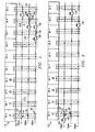
- FIGURE 3 illustrates a further embodiment of the present invention that includes spatially distributed or staggered segmentation points of similar track segments. This type of staggering improves routability in the user-programmable integrated circuit 60.
- the staggered user-programmable integrated circuit 60 includes logic modules LMO through LM5, each having associated input pins A, B, and C.
- segmentation transistors such as transistors 62, 64, 66, 68, 70 and 72.
- the segmentation transistors may be placed at other points within user-programmable integrated circuit 60.
- the segmentation transistors of FIGURE 23 are at different points along the various tracks. The result is an improvement in the general routability of user-programmable integrated circuit 60 or the similar user programmable integrated circuit 10 of FIGURE 1.
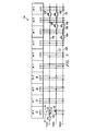
- FIGURE 4 shows another example of long segments that have different lengths.
- the circuit diagrams of FIGURES 1 through 7 show very simple three-input logic modules to illustrate this invention.
- typical logic modules may have six to ten inputs or more in antifuse-based FPGA architectures.
- the sparsely-populated segments may have more than one potential populated input antifuse location.
- circuitry architects may apply information from the macro library and the associated statistics of macro utilization to determine which logic module inputs to most frequently populate or, conversely, which logic module inputs to depopulate more frequently. At the same time, designers should consider minimizing the reductions in routability due to depopulation.
- User-programmable integrated circuit 80 of FIGURE 4 illustrates dense segments of various lengths.
- dense segment 82 appears on track 0 and through segmentation transistor 84 joins track 0 portion 86.
- segmentation transistor 88 separates track 1 portion 90 from the short dense segment 92.
- sparsely populated segment 86 of track 0 and sparsely populated segment 90 of track 1 have different lengths.
- densely populated segment 82 and densely populated segment 92 In a similar fashion, segmentation transistors 94 and 96 separate track 2 into three segments. Two segments are sparsely populated, i.e., segments 98 and 100, while short, densely populated segment 102 is isolated by segmentation transistors 94 and 96.
- FIGURE 5 shows user-programmable integrated circuit 10 which is similar to that of FIGURE 4 and illustrates the desirability of distributing the logic module inputs that are to be populated on sparsely populated segments.
- segmentation transistor 114 separates sparsely populated segment 112 from densely populated segment 116.
- segmentation transistors 122 and 124 respectively, separate sparsely populated segments 118 and 120 from short, densely populated segment 126.
- segmentation transistors 128 and 130 separate, respectively, selectively depopulated segments 132 and 134 from densely populated short segment 136.
- User-programmable integrated circuit 110 therefore, achieves a desired effect of providing a sparse segment to access two different functional inputs. This may be important for architectures that use logic modules (such as multiplexer-based logic modules) which have asymmetric input functionality. For example, if the logic modules were to perform a two-input NAND gate, the inputs may be required at input pins B and C of the logic module such that input pins A and C may not achieve the desired result. Shifting populated inputs around on a segment allows the placement tool to shift the macro instance into routable positions.
- logic modules such as multiplexer-based logic modules
- FIGURE 6 appears yet a further embodiment of user-programmable integrated circuit 140 that includes segmentation transistors 142 on track 0, segmentation transistor 144, and segmentation transistor 146 on track 2.
- the embodiment of FIGURE 6 illustrates the concept of variable depopulation within an individual segment.
- One of the concepts that user-programmable integrated circuit 140 of FIGURE 6 embodies is that of increasing routability while still achieving significant reduction in the number of antifuses and their associated parasitic leakage current and capacitance characteristics.
- User-programmable integrated circuit 140 allows a segment to traverse a significant distance between a driving node such as LMO and a destination point such as LM8 or LM9 as they connect with track 0, for example.
- the signal may be required very infrequently. As such, this distance is selectively depopulated. Increasing the density of the antifuse population near the ends of the segment, the probability is increased that the segment's signal will be available to the required logic module input. This also may reduce the frequency of requiring a short, dense segment being connected to the long, sparse segment.
- FIGURE 7 includes a long track 0 segmentation transistor 152 that connects to densely populated portions of long segment 154. These densely populated portions go to LMO and LM1. Another densely populated portion of long segment 154 appears at LM7 and LM8. Separating LM8 from LM9, which is also densely populated is segmentation transistor 156. On track 1 appears densely populated segment LMO that is sparsely populated until the densely populated portion associated with LM6 and LM7. Segmentation transistor 158 separates LM7 and LM8 connections along track 1, while segmentation transistor 160 separates LM8 and LM9 antifuses along track 1.
- segmentation transistor 164 separates LM6 and LM7, while segmentation transistor 166 separates short segment 168 from densely populated segment 170.
- User-programmable integrated circuit 150 of FIGURE 7 therefore, illustrates the combination of including a variably depopulated long sparse segment having densely populated portions or segments ends together with an adjoining short, densely populated segments.
- the short, densely populated segments of user-programmable integrated circuit 150 of FIGURE 7 may be of variable length.
- FIGURE 8 shows yet a further embodiment of the present invention in the form of user-programmable integrated circuit 180 that shows how inventive concepts of the various embodiments may be employed in both X and Y dimensions of a routing architecture.
- LMO has input pins A, B, and C that, respectively, have antifuse links 182, 184, and 186 that associate, again respectively, with track 0, track 1 and track 2. These are the above-described connections that appear in the y direction. Also, however, output pin Q may exit LMO to intersect vertical tracks 188 and 190 and antifuses 192 and 194, respectively.
- Vertical tracks 188 and 190 may also intersect at antifuses 196 and 198 with track 0, and antifuses 200 and 202 with track 1 and, for example at antifuse 204 with track 2.
- segmentation transistors 206 and 208 may, for example, isolate vertical tracks 188 and 190 from vertical track portions 210 and 212 that may connect to output pin Q of LM4 via antifuse links 214 and 216.
- User-programmable integrated circuit 180 attempts to illustrate that the ideas of the various embodiments may be employed in both the x and y dimensions of a routing architecture.
- the simple case of user-programmable integrated circuit 180 shows the long sparse segments as only two logic module rows. The densely populated short segments are a single row tall. In practical cases, the vertical segment lengths would be longer and may vary.
- the output shown in FIGURE 8 is shown as fusible to the two vertical segments in each column, the output could be hard connected to either vertical or horizontal segments while still being fusible to additional segments running in the same direction or onto external segments adjoining the output segments.
- a technical advantage of the present invention is that it provides a way of differentiating between connectors in an integrated electronic circuit for which leakage and capacitance from antifuses contribute more than a desirable amount to the total leakage and capacitance of the connectors.
- Another technical advantage of the present invention is that it may be used for a variety of programmable logic devices including, for example, a field programmable gate array (FPGA) to optimize the FPGA's programmability while minimizing the undesirable effects of leakage and capacitance associated with the antifuses that connect the FPGA logic modules to various tracks.
- FPGA field programmable gate array
- Another technical advantage of the present invention is that it permits selecting particular antifuses to depopulate from a candidate routing architecture according to the potential macros that may be used to program the integrated electronic circuit.
- the present invention includes various embodiments such as a method and system for reducing the total leakage and capacitance in a user-programmable integrated electronic circuit.
- the user-programmable integrated circuit having conductors that may be connected to one another and to functional circuit blocks by programming the user-programmable antifuses that connect to the conductors and to the functional circuit blocks to form the electronic circuit.
- the steps of the method include segregating the conductors into at least two segments each having antifuses.
- the two conductor segments include a first segment and a second segment.
- the first segment has a sufficiently large number of potential antifuse sites so that if antifuses were located at each of the potential antifuse sites, then the antifuses would contribute a larger proportion to the total leakage current and capacitance of the first segment than do the antifuses of the second segment contribute to the total leakage current and capacitance of the second segment.
- the method further includes the step of depopulating selected ones of the potential antifuse location of the first segment.
- the selected antifuses being selected to minimally reduce programmability of the user-programmable integrated circuit while optimally reducing the total leakage current and capacitance of the first design group for, thereby reducing the total leakage capacitance of the electronic circuit.
Applications Claiming Priority (2)
| Application Number | Priority Date | Filing Date | Title |
|---|---|---|---|
| US17823094A | 1994-01-06 | 1994-01-06 | |
| US178230 | 1998-10-23 |
Publications (2)
| Publication Number | Publication Date |
|---|---|
| EP0667679A1 true EP0667679A1 (de) | 1995-08-16 |
| EP0667679B1 EP0667679B1 (de) | 1997-06-25 |
Family
ID=22651736
Family Applications (1)
| Application Number | Title | Priority Date | Filing Date |
|---|---|---|---|
| EP19940309766 Expired - Lifetime EP0667679B1 (de) | 1994-01-06 | 1994-12-23 | Verbindungsarchitekturen |
Country Status (3)
| Country | Link |
|---|---|
| EP (1) | EP0667679B1 (de) |
| JP (1) | JPH07282127A (de) |
| DE (1) | DE69403949T2 (de) |
Cited By (1)
| Publication number | Priority date | Publication date | Assignee | Title |
|---|---|---|---|---|
| US7107566B1 (en) * | 2004-01-22 | 2006-09-12 | Altera Corporation | Programmable logic device design tools with gate leakage reduction capabilities |
Citations (2)
| Publication number | Priority date | Publication date | Assignee | Title |
|---|---|---|---|---|
| EP0469728A1 (de) * | 1990-08-01 | 1992-02-05 | Actel Corporation | Programmierbare Verbindungsarchitektur |
| US5250464A (en) * | 1992-03-11 | 1993-10-05 | Texas Instruments Incorporated | Method of making a low capacitance, low resistance sidewall antifuse structure |
-
1994
- 1994-12-23 DE DE1994603949 patent/DE69403949T2/de not_active Expired - Lifetime
- 1994-12-23 EP EP19940309766 patent/EP0667679B1/de not_active Expired - Lifetime
-
1995
- 1995-01-06 JP JP7000830A patent/JPH07282127A/ja active Pending
Patent Citations (2)
| Publication number | Priority date | Publication date | Assignee | Title |
|---|---|---|---|---|
| EP0469728A1 (de) * | 1990-08-01 | 1992-02-05 | Actel Corporation | Programmierbare Verbindungsarchitektur |
| US5250464A (en) * | 1992-03-11 | 1993-10-05 | Texas Instruments Incorporated | Method of making a low capacitance, low resistance sidewall antifuse structure |
Non-Patent Citations (3)
| Title |
|---|
| A. EL GAMAL ET AL.:: "An Architecture for Electrically Configurable Gate Arrays", IEEE JOURNAL OF SOLID-STATE CIRCUITS, vol. 24, no. 2, April 1989 (1989-04-01), NEW YORK, US, pages 394 - 398, XP000004546, DOI: doi:10.1109/4.18600 * |
| A. HAINES:: "Field-programmable gate array with non-volatile configuration", MICROPROCESSORS &MICROSYSTEMS, vol. 13, no. 5, June 1989 (1989-06-01), LONDON, GB, pages 305 - 312, XP000119062, DOI: doi:10.1016/0141-9331(89)90086-0 * |
| W. ANDREWS:: "User-configurable arrays bridge gap between gate arrays and PLDs", COMPUTER DESIGN, vol. 27, no. 14, 1 August 1988 (1988-08-01), LITTLETON, MA, US, pages 32 - 36, XP000104723 * |
Cited By (1)
| Publication number | Priority date | Publication date | Assignee | Title |
|---|---|---|---|---|
| US7107566B1 (en) * | 2004-01-22 | 2006-09-12 | Altera Corporation | Programmable logic device design tools with gate leakage reduction capabilities |
Also Published As
| Publication number | Publication date |
|---|---|
| DE69403949D1 (de) | 1997-07-31 |
| EP0667679B1 (de) | 1997-06-25 |
| DE69403949T2 (de) | 1997-12-18 |
| JPH07282127A (ja) | 1995-10-27 |
Similar Documents
| Publication | Publication Date | Title |
|---|---|---|
| US5600265A (en) | Programmable interconnect architecture | |
| US5187393A (en) | Reconfigurable programmable interconnect architecture | |
| US5172014A (en) | Programmable interconnect architecture | |
| US6828824B2 (en) | Heterogeneous interconnection architecture for programmable logic devices | |
| US5191241A (en) | Programmable interconnect architecture | |
| US5132571A (en) | Programmable interconnect architecture having interconnects disposed above function modules | |
| US4910417A (en) | Universal logic module comprising multiplexers | |
| US4873459A (en) | Programmable interconnect architecture | |
| Rose et al. | Architecture of field-programmable gate arrays | |
| US5038192A (en) | Gate array cell having FETs of different and optimized sizes | |
| US5631578A (en) | Programmable array interconnect network | |
| EP0463746B1 (de) | Segmentierung von Spuren in FPGA Verdrahtungs-Kanälen | |
| US4207556A (en) | Programmable logic array arrangement | |
| US5777887A (en) | FPGA redundancy | |
| US20040105207A1 (en) | Via programmable gate array interconnect architecture | |
| EP0612153A1 (de) | FPGA mit verteilter Schaltmatrix | |
| US5378941A (en) | Bipolar transistor MOS transistor hybrid semiconductor integrated circuit device | |
| US5341043A (en) | Series linear antifuse array | |
| US6630842B1 (en) | Routing architecture for a programmable logic device | |
| US5166547A (en) | Programmable DCVS logic circuits | |
| KR930003838B1 (ko) | 유니트 블록(unit block)구조를 갖는 바이폴라 집적회로 | |
| US5469078A (en) | Programmable logic device routing architecture | |
| EP0667679A1 (de) | Verbindungsarchitekturen | |
| KR0150778B1 (ko) | 반도체 집적회로 장치 및 그 설계방법 | |
| JP3202601B2 (ja) | 論理回路及び半導体集積回路配列 |
Legal Events
| Date | Code | Title | Description |
|---|---|---|---|
| PUAI | Public reference made under article 153(3) epc to a published international application that has entered the european phase |
Free format text: ORIGINAL CODE: 0009012 |
|
| AK | Designated contracting states |
Kind code of ref document: A1 Designated state(s): DE FR GB IT NL |
|
| 17P | Request for examination filed |
Effective date: 19960216 |
|
| GRAG | Despatch of communication of intention to grant |
Free format text: ORIGINAL CODE: EPIDOS AGRA |
|
| 17Q | First examination report despatched |
Effective date: 19960729 |
|
| GRAH | Despatch of communication of intention to grant a patent |
Free format text: ORIGINAL CODE: EPIDOS IGRA |
|
| GRAH | Despatch of communication of intention to grant a patent |
Free format text: ORIGINAL CODE: EPIDOS IGRA |
|
| GRAA | (expected) grant |
Free format text: ORIGINAL CODE: 0009210 |
|
| AK | Designated contracting states |
Kind code of ref document: B1 Designated state(s): DE FR GB IT NL |
|
| REF | Corresponds to: |
Ref document number: 69403949 Country of ref document: DE Date of ref document: 19970731 |
|
| EN | Fr: translation not filed | ||
| PLBE | No opposition filed within time limit |
Free format text: ORIGINAL CODE: 0009261 |
|
| STAA | Information on the status of an ep patent application or granted ep patent |
Free format text: STATUS: NO OPPOSITION FILED WITHIN TIME LIMIT |
|
| ET | Fr: translation filed | ||
| REG | Reference to a national code |
Ref country code: FR Ref legal event code: RN Ref country code: FR Ref legal event code: FC |
|
| 26N | No opposition filed | ||
| REG | Reference to a national code |
Ref country code: GB Ref legal event code: IF02 |
|
| PGFP | Annual fee paid to national office [announced via postgrant information from national office to epo] |
Ref country code: IT Payment date: 20061231 Year of fee payment: 13 |
|
| PG25 | Lapsed in a contracting state [announced via postgrant information from national office to epo] |
Ref country code: IT Free format text: LAPSE BECAUSE OF NON-PAYMENT OF DUE FEES Effective date: 20071223 |
|
| PGFP | Annual fee paid to national office [announced via postgrant information from national office to epo] |
Ref country code: NL Payment date: 20091222 Year of fee payment: 16 |
|
| PGFP | Annual fee paid to national office [announced via postgrant information from national office to epo] |
Ref country code: GB Payment date: 20091106 Year of fee payment: 16 Ref country code: FR Payment date: 20091215 Year of fee payment: 16 |
|
| PGFP | Annual fee paid to national office [announced via postgrant information from national office to epo] |
Ref country code: DE Payment date: 20091230 Year of fee payment: 16 |
|
| REG | Reference to a national code |
Ref country code: NL Ref legal event code: V1 Effective date: 20110701 |
|
| GBPC | Gb: european patent ceased through non-payment of renewal fee |
Effective date: 20101223 |
|
| REG | Reference to a national code |
Ref country code: FR Ref legal event code: ST Effective date: 20110831 |
|
| PG25 | Lapsed in a contracting state [announced via postgrant information from national office to epo] |
Ref country code: FR Free format text: LAPSE BECAUSE OF NON-PAYMENT OF DUE FEES Effective date: 20110103 |
|
| REG | Reference to a national code |
Ref country code: DE Ref legal event code: R119 Ref document number: 69403949 Country of ref document: DE Effective date: 20110701 |
|
| PG25 | Lapsed in a contracting state [announced via postgrant information from national office to epo] |
Ref country code: GB Free format text: LAPSE BECAUSE OF NON-PAYMENT OF DUE FEES Effective date: 20101223 Ref country code: DE Free format text: LAPSE BECAUSE OF NON-PAYMENT OF DUE FEES Effective date: 20110701 |
|
| PG25 | Lapsed in a contracting state [announced via postgrant information from national office to epo] |
Ref country code: NL Free format text: LAPSE BECAUSE OF NON-PAYMENT OF DUE FEES Effective date: 20110701 |