EP0664508B1 - Datenprozessor zur leistungsfähigen Bitübertragung und Verfahren dafür - Google Patents
Datenprozessor zur leistungsfähigen Bitübertragung und Verfahren dafür Download PDFInfo
- Publication number
- EP0664508B1 EP0664508B1 EP95100682A EP95100682A EP0664508B1 EP 0664508 B1 EP0664508 B1 EP 0664508B1 EP 95100682 A EP95100682 A EP 95100682A EP 95100682 A EP95100682 A EP 95100682A EP 0664508 B1 EP0664508 B1 EP 0664508B1
- Authority
- EP
- European Patent Office
- Prior art keywords
- address
- destination
- source
- bit
- operand
- Prior art date
- Legal status (The legal status is an assumption and is not a legal conclusion. Google has not performed a legal analysis and makes no representation as to the accuracy of the status listed.)
- Expired - Lifetime
Links
Images


Classifications
-
- G—PHYSICS
- G06—COMPUTING OR CALCULATING; COUNTING
- G06F—ELECTRIC DIGITAL DATA PROCESSING
- G06F9/00—Arrangements for program control, e.g. control units
- G06F9/06—Arrangements for program control, e.g. control units using stored programs, i.e. using an internal store of processing equipment to receive or retain programs
- G06F9/30—Arrangements for executing machine instructions, e.g. instruction decode
- G06F9/30003—Arrangements for executing specific machine instructions
- G06F9/30007—Arrangements for executing specific machine instructions to perform operations on data operands
- G06F9/30018—Bit or string instructions
-
- G—PHYSICS
- G06—COMPUTING OR CALCULATING; COUNTING
- G06F—ELECTRIC DIGITAL DATA PROCESSING
- G06F9/00—Arrangements for program control, e.g. control units
- G06F9/06—Arrangements for program control, e.g. control units using stored programs, i.e. using an internal store of processing equipment to receive or retain programs
- G06F9/30—Arrangements for executing machine instructions, e.g. instruction decode
- G06F9/30003—Arrangements for executing specific machine instructions
- G06F9/30007—Arrangements for executing specific machine instructions to perform operations on data operands
- G06F9/30032—Movement instructions, e.g. MOVE, SHIFT, ROTATE, SHUFFLE
-
- G—PHYSICS
- G06—COMPUTING OR CALCULATING; COUNTING
- G06F—ELECTRIC DIGITAL DATA PROCESSING
- G06F9/00—Arrangements for program control, e.g. control units
- G06F9/06—Arrangements for program control, e.g. control units using stored programs, i.e. using an internal store of processing equipment to receive or retain programs
- G06F9/30—Arrangements for executing machine instructions, e.g. instruction decode
- G06F9/30145—Instruction analysis, e.g. decoding, instruction word fields
- G06F9/3016—Decoding the operand specifier, e.g. specifier format
- G06F9/30167—Decoding the operand specifier, e.g. specifier format of immediate specifier, e.g. constants
Definitions
- This invention relates generally to data processors, and more particularly, to data processors for communications systems and the like.
- DSPs digital signal processors
- MAC dedicated multiplier/accumulator
- bit interleaving and de-interleaving operations in order to reduce the effect of errors due to noise bursts.
- bit interleaving operations provide increased immunity to noise bursts by spreading the data stream over several frames prior to transmission.
- noise burst which may corrupt the data in one transmitted frame, is likely to only affect bits that are widely scattered in the original data stream.
- the receiver may thus be able to recover the correct data despite the noise burst.
- a typical data processor first calculates the address of the operand which contains the source bit, then calculates the address of the operand which contains the destination bit position in which the source bit is to be written, fetches the source operand, applies a mask to the source operand to obtain the bit, writes the bit to the appropriate bit position of the destination operand, and stores the destination operand.
- This sequence requires approximately 6 to 10 instruction cycles on known microprocessors to complete. During long data transmission or reception sequences, the number of instruction cycles becomes excessive, resulting in increased CPU architectural complexity, clock speed, and higher power consumption. The high power consumption further decreases battery life in battery-based applications.
- bit move instructions which improve their performance over conventional data processors which do not have bit move instructions.
- further improvement is desirable.
- known processors with bit movement instructions must first compute the address of the processor word which contains the desired source bit and the address (position) of that source bit within the word.
- a similar computation must determine the address of the processor word which contains the destination bit and the address (position) of the destination bit within that word.
- the addressed source bit is moved into the address destination bit.
- the extract bit field (BFEXT) instruction moves a specified bit(s) in a source operand to the low-order bit(s) of a register.
- the insert bit field (BFINS) instruction moves the low-order bit(s) of this register to a specified position in a destination operand.
- EP 0 382 246 discloses a bit addressing system which may be used for an instruction requiring bit addressing, such as extraction, insertion, or comparison.
- the system generates an effective byte address and an effective bit offset address using a byte base address and a bit displacement from the byte base address.
- K.L. Kloker in "The Motorola DSP56000 Digital Signal Processor," IEEE Micro, vol. 6, no. 6, December 1, 1986, pp. 29-48 discloses a digital signal processing system having an address generator which generates two independent memory addresses each instruction cycle.
- the present invention provides, in one form, a data processor with an efficient bit move capability, including an instruction decoder, an address generator, a bus controller, and an execution unit, as recited in claim 1.
- the present invention provides a method for efficiently moving bits between operands in a data processor in response to receiving a bit move instruction, as recited in claim 8.
- FIG. 1 illustrates in block diagram form a general bit movement operation.
- FIG. 2 illustrates in block diagram form a particular bit movement operation.
- FIG. 3 illustrates in block diagram form a data processor with an efficient bit move capability according to the present invention.
- FIG. 4 illustrates in partial block and partial logic diagram form one portion of the data processor of FIG. 3.
- FIG. 5 illustrates in block diagram form a portion of the execution unit of FIG. 3 for performing bit move instructions.
- FIG. 1 illustrates in block diagram form a general bit movement operation.
- This bit movement operation is illustrated in the context of a memory space 20 having a contiguous source memory space 21 and a contiguous destination memory space 25.
- Source memory space 21 and destination memory space 25 are not necessarily restricted to occupying separate spaces.
- Source memory space 21 includes n operands each having a given width such as 8-bit (byte), 16-bit (word), 32-bit (long word), etc.
- a source bit 23 is identified as the bit to be moved.
- source bit 23 may be located at any bit position in any of the operands in source memory space 21.
- destination memory space 25 includes n operands of the given width.
- a destination bit 27 is identified as the bit address to which source bit 23 is to be moved. Depending on the sequence of bit movements to be performed, destination bit 27 may be located at any bit position in any of the destination operands. In FIG. 1, an arrow represents a bit movement operation from source bit 23 to destination bit 27.
- FIG. 2 illustrates in block diagram form a particular bit movement operation.
- This bit movement operation is an interleaving operation specified in the Groupe Speciale Mobile (GSM) cellular telephone standard known as the Stand-alone Dedicated Control Channel (SDCCH).
- GSM Groupe Speciale Mobile
- SDCCH Stand-alone Dedicated Control Channel
- the SDCCH interleaving example is illustrated in the context of a memory space 30 having a contiguous control buffer memory space 31 and four contiguous buffers 32-35.
- Conventional processors do not have the capability to efficiently implement the SDCCH interleaving scheme shown above, because they do not provide the indexed modulo addressing modes combined with the required bit movement capability within a single instruction.
- FIG. 3 illustrates in block diagram form a data processor with an efficient bit move capability 40 according to the present invention.
- Data processor 40 includes generally an instruction decoder 41, an address generation unit (AGU) 42, a register file 43, a bus controller 44, and an execution unit 45.
- AGU address generation unit
- data processor 40 is connected indirectly to a memory 50 through a source address bus (SAB) 51, a source data bus (SDB) 52, a destination address bus (DAB) 53, and a destination data bus (DDB) 54.
- SAB source address bus
- SDB source data bus
- DDB destination address bus
- DDB destination data bus
- memory 50 and buses 51-54 may be external to data processor 40.
- Instruction decoder 41 has an input for receiving data labelled "PDATA", which represents any of a number of instructions to be executed by data processor 40.
- PDATA data labelled "PDATA”
- the actual set of instructions that instruction decoder 41 responds to will vary from embodiment to embodiment but typically includes data movement instructions, arithmetic and logical instructions, and the like.
- instruction decoder 41 is responsive to a bit movement instruction designated an "MBIT" instruction, which copies a selected bit within a source memory space into a selected bit position within a destination memory space, such as during the GSM SDDCH control frame data interleaving algorithm illustrated in FIG. 2.
- MBIT bit movement instruction
- instruction decoder 41 provides three decoded control signals, labelled "SOURCE UPDATE”, “DESTINATION UPDATE”, and a control bit also labelled "MBIT”.
- AGU 42 is an address generator with modulo-addressing capabilities which allow it to efficiently perform digital signal processing (DSP) functions.
- AGU 42 has two portions capable of performing independent source and destination address calculation. A first portion is responsive to signal SOURCE UPDATE in order to update a present source address to a next source address according to a source offset and a source modulus value. Likewise, a second portion is responsive to signal DESTINATION UPDATE in order to update a present destination address to a next destination address according to a destination offset and a destination modulus value.
- AGU 42 is connected to memory 50 via SDB 52 and DDB 54 to receive the initial addresses and offset and modulus values for use in the source and destination address updates.
- AGU 42 provides the present calculated address values, labelled "PRESENT SOURCE ADDRESS” and "PRESENT DESTINATION ADDRESS”, to register file 43, which stores these values for presentation to bus controller 44.
- AGU 42 updates these address while bus controller 44 is using them, i.e., performs a post-update. However, in other embodiments, AGU 42 could perform a pre-update as well.
- Bus controller 44 receives the PRESENT SOURCE ADDRESS and PRESENT DESTINATION ADDRESS from register file 43, and provides two corresponding operand addresses, labelled "SOURCE OPERAND ADDRESS” and "DESTINATION OPERAND ADDRESS” to SAB 51 and DAB 53, respectively. In addition, bus controller 44 provides additional control signals which are not illustrated in FIG. 3. Bus controller 44 provides the SOURCE OPERAND ADDRESS and DESTINATION OPERAND ADDRESS differently according to the type of instruction. During most instructions, the SOURCE OPERAND ADDRESS and DESTINATION OPERAND ADDRESS are identical to the PRESENT SOURCE ADDRESS and PRESENT DESTINATION ADDRESS, respectively.
- bus controller 44 recognizes that the PRESENT SOURCE ADDRESS and PRESENT DESTINATION ADDRESS represent bit addresses in response to signal MBIT.
- bus controller 44 separates the PRESENT SOURCE ADDRESS into two fields, the SOURCE OPERAND ADDRESS and a field labelled "SOURCE BIT FIELD", which bus controller 44 provides to execution unit 45.
- bus controller 44 separates the PRESENT DESTINATION ADDRESS into two fields, the DESTINATION OPERAND ADDRESS and a field labelled "DESTINATION BIT FIELD", which bus controller 44 provides to execution unit 45.
- bus controller 44 divides the present address by the number of bits in the operand to provide the operand address.
- the bit field is an encoded signal to select one bit of a number of bits equal to the number of bits per operand.
- the operand address would be equal to the present address divided by 8, and the bit field would be the three least significant bits of the present address.
- the number of bits per operand is completely arbitrary, although bus controller 44 and execution unit 45 can be implemented more easily with an operand size which is an integer power of two.
- data processing systems most frequently organize memory into byte, 16-bit (word), and 32-bit (long word) sizes.
- Execution unit 45 has inputs for receiving the SOURCE BIT FIELD and the DESTINATION BIT FIELD, a control input for receiving signal MBIT, and bidirectional connections to SDB 52 for conducting a data element labelled "SOURCE OPERAND", and to DDB 54 for conducting a data element labelled "DESTINATION OPERAND”.
- bus controller 44 provides the SOURCE OPERAND ADDRESS and control signals, not shown, to access the SOURCE OPERAND, which is received by execution unit 45.
- bus controller 44 provides the DESTINATION OPERAND ADDRESS and control signals, not shown, to access the DESTINATION OPERAND, which is also received by execution unit 45.
- Execution unit 45 then copies a bit of the SOURCE OPERAND selected by the SOURCE BIT FIELD, into a bit position of the DESTINATION OPERAND selected by the DESTINATION BIT FIELD.
- bus controller 44 again provides the DESTINATION OPERAND ADDRESS and control signals to store the result of the MBIT instruction as an updated DESTINATION OPERAND, provided by execution unit 45.
- the overall advantages of the MBIT capability of data processor 40 are to efficiently combine source and destination operand addresses and bit position addresses with bit movement execution in one machine instruction which has the same execution time as all other instructions of the processor.
- the MBIT instruction effectively converts a byte addressable processor into a bit addressable processor for source and destination addresses combined with bit movement execution.
- Data processor 40 implements one bit interleave operation in each machine cycle. In the same cycle, the positions of the subsequent source and destination bit locations are calculated and updated. In contrast, known data processors in general, consume a large number of CPU cycles during each interleave operation generating the byte and bit locations for the source and destination operands. Depending on the processor used, typically 6 to 10 cycles are required to perform a single bit interleave operation.
- a code segment illustrating the use of the MBIT instruction to perform the SDCCH interleaving operation is shown below: where "mov” represents a data movement instruction from memory to an on-chip register, "#” represents immediate data, “r j " represents the jth register, “DO” represents a do loop, “rep” represents a repeat instruction, and “nop” represents a no-operation instruction (which still allows address register updates).
- Memory system 20, which stores the MBIT "SOURCE” and "DESTINATION” operands, can be integrated on the silicon, located off-chip, or be partly on-chip and partly off-chip.
- AGU 42 The advantage of placing the address separation in bus controller 44, is that alternate address generators or sources can be used without affecting the structure of AGU 42 itself.
- Fixed address data port(s) is one example where the address could be provided by a register or read-only memory (ROM) as a register indirect address or absolute address. This would be advantageous in a multi-processor system.
- FIG. 4 illustrates in partial block and partial logic diagram form one portion of data processor 40 of FIG. 3.
- This portion of data processor 40 further illustrates AGU 42, register file 43, and bus controller 44, and the same reference numbers are used to identify these blocks in FIG. 4 as well.
- AGU 42 includes generally three AGUs, namely an "S1" AGU 60, an "S2" AGU 61, and a "D" AGU 62.
- S1 AGU 60 is chosen as the source AGU
- another one of these AGUs preferably S2 AGU 61
- Each AGU performs an identical function, of which only AGU 60 will be illustrated in detail.
- AGU 60 includes an address pointer register 64, an offset register 65, a modulus register 66, a summing device 67, and an division device 68.
- S1 AGU 60 is operative in response to a signal labelled "S1 UPDATE", which in the illustrated embodiment is the same as signal SOURCE UPDATE.
- Address pointer register 64 includes either the initial address or the address value calculated at the last update, and provides this value to one input of summing device 67.
- Offset register 65 provides the present offset, and modulus register 66 the present modulus. Note that the offset and modulus values may be updated from time to time.
- Summing device 67 adds the offset provided by offset register 65 to the present address value provided by address pointer register 64, to provide a sum thereof. This sum is then brought within the range specified by the modulus value in divider 68, which divides the sum of the address plus the offset by the modulus value.
- AGU 61 may be implemented by well-known modulo adjusting circuitry.
- the SDCCH algorithm requires the MBIT instruction to be used in the following form: MBIT (r a +64,%456),(r b +2) where r a and r b refer to internal registers in the register file of data processor 40.
- the first part of this instruction accesses the source bit using the indirect address specified by register r a , and subsequently calculates the position of the next source bit by adding 64 to the present r a value according to a modulus of 456.
- the second part of the instruction stores the destination bit using the indirect bit position specified by register r b , and calculates the position of the next destination bit by adding 2 to the present r b value.
- Each of AGUs 60-62 provide an address value having (m + 1) bits to register file 43.
- Register file 43 includes three registers 70-72 for storing the output of AGUs 60-62, respectively.
- the outputs of registers 70-72 are thereafter available for use in bus controller 44.
- Bus controller 44 includes three shifter/multiplexers (SHIFT/MUXes) 80-82.
- SHIFT/MUXes 80-82 each have inputs for receiving outputs of a corresponding one of registers 70-72, control inputs for receiving signal MBIT, inputs for receiving a corresponding index labelled "S1 INDEX", "S2 INDEX”, and "D INDEX", respectively, and outputs for providing a corresponding operand address.
- SHIFT/MUXes 80 and 81 have outputs for providing a corresponding bit field.
- SHIFT/MUX 80 includes a bit shifter 84 and a multiplexer 85.
- Bit shifter 84 converts a present address labelled the "PRESENT S1 ADDRESS", a bit address, to a "CONVERTED S1 ADDRESS", an (m + 1)-bit address accessing 8-bit (byte) operands.
- Bit shifter 84 in essence divides the PRESENT S1 ADDRESS by 8, by mapping the (m + 1 - n) most significant bits of the PRESENT S1 ADDRESS to bit positions (m + 1 - n) to 0 of the CONVERTED S1 ADDRESS.
- Bit shifter 84 also maps n-bit S1 INDEX onto the n most-significant bit positions of the CONVERTED S1 ADDRESS.
- MUX 85 has a first input for receiving the CONVERTED S1 ADDRESS, a second input for receiving the PRESENT S1 ADDRESS, a control input for receiving signal MBIT, and an output for providing the S1 OPERAND ADDRESS.
- S1 OPERAND ADDRESS is the same as the SOURCE OPERAND ADDRESS.
- the S1 BIT FIELD which in the illustrated embodiment is the same as the SOURCE BIT FIELD, is taken as the n least significant bits of the PRESENT S1 ADDRESS.
- AGU 42 is a conventional circular buffer AGU.
- the modest addition of the shifter/multiplexer in bus controller 44 facilitates the implementation of the MBIT instruction by separating the operand address portion from the bit field address portion of the present address as calculated by the AGU.
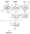
- FIG. 5 illustrates in block diagram form a portion of execution unit 45 of FIG. 3 for performing bit move instructions, designated MBIT portion 90.
- MBIT portion 90 includes those blocks of execution unit 45 relevant to the MBIT instruction. Note that execution unit 45 also performs additional operations including multiplications, multiply-and-accumulates, additions, and the like. However, the blocks which perform these conventional operations are not shown in FIG. 5.
- MBIT portion 90 is operative to complete the MBIT instruction in one clock cycle. This clock cycle is divided in half by two nonoverlapping clock signals labelled "CLK1" and "CLK2".
- a register 91 labelled “S2 OPERAND ADDRESS REGISTER” latches the (m + 1)-bit S2 OPERAND ADDRESS from bus controller 44 in response to clock signal CLK1.
- a latch portion 92 includes a selectable 1-bit latch receiving one of the (m + 1) bits in the S1 OPERAND ADDRESS, selected by (m + 1) corresponding select signals, and is operative in response to signal CLK1.
- a decoder 93 provides these select signals by decoding the n-bit S1 BIT FIELD into (m + 1) select signals. Decoder 93 also has a control input for receiving signal MBIT and a clock input for receiving signal CLK1.
- Register 91 and latch portion 92 each has an (m + 1)-bit output which is provided to corresponding inputs of a set of (m + 1) 2-to-1 MUXes 94.
- MUXes 94 also have (m + 1) control inputs for receiving corresponding ones of a set of (m + 1) select signals.
- a decoder 95 provides these select signals by decoding the n-bit S2 BIT FIELD into (m + 1) select signals.
- Decoder 93 also has a control input for receiving signal MBIT and a clock input for receiving signal CLK2.
- MUXes 94 have an (m + 1)-bit output connected to an input of an output drivers block 96.
- Output drivers block 96 has an output for providing an (m + 1)-bit output labelled "RESULT", and a clock input for receiving signal CLK2.
- MBIT portion 90 is a dedicated hardware module for the MBIT instruction which is simple and occupies only a small amount of integrated circuit area.
- the instruction decode and bit field decodes occur in the clock phase prior to the execution clock. This allows the destination operand and the selected bit in the source operand to be latched in the first phase of the execution clock cycle (CLK1). Then, in the second phase of the execution clock cycle (CLK2), the latched bit of the source operand is multiplexed into the selected bit of the destination operand, and the result is driven out through output drivers 96. This operation results in a single-clock execution of moving the addressed bit in the source operand into the addressed bit position of the destination operand.
- the combined effect of the AGU, bus controller, and execution unit achieve an efficient implementation of the bit movement function which results in fewer processor cycles being required to complete the data interleaving/deinterleaving requirement of the GSM standard. Since all transmitted data are interleaved in GSM, the MBIT capability of the processor allows for substantially fewer instruction cycles and correspondingly lower power consumption which is critical to a battery-powered application.
Landscapes
- Engineering & Computer Science (AREA)
- Software Systems (AREA)
- Theoretical Computer Science (AREA)
- Physics & Mathematics (AREA)
- General Engineering & Computer Science (AREA)
- General Physics & Mathematics (AREA)
- Executing Machine-Instructions (AREA)
- Microcomputers (AREA)
Claims (10)
- Datenprozessor (40) mit leistungsfähiger Bitübertragung, der einen Befehlsdecodierer (41) mit einem Eingang zum Empfang eines Befehls einer Vielzahl von Befehlen, einen Adressengenerator (42), der mit dem Befehlsdecodierer (41) gekoppelt ist, mit Ursprungs- (60) und Ziel-(61) Teilen davon, einen Buscontroller (44) und eine Ausführungseinheit (45) aufweist, die mit Ursprungs- (51) und Ziel- (53) Datenwegen zum Empfang von Ursprungs- und Zieloperanden an Adressen, die jeweils durch Ursprungs- beziehungsweise Zieloperandenadressen dargestellt werden, gekoppelt ist, dadurch gekennzeichnet, dass:die Vielzahl von Befehlen einen Bitübertragungsbefehl umfasst, wobei der Befehlsdecodierer (41) einen Ausgang zum Bereitstellen erster, zweiter und dritter decodierter Signale als Antwort auf den Bitübertragungsbefehl aufweist;der Ursprungsteil (60) eine derzeitige Ursprungsadresse bereitstellt und die derzeitige Ursprungsadresse gemäß einem Ursprungsoffset (65) aktualisiert, als Antwort auf das erste decodierte Signal, wobei die derzeitige Ursprungsadresse eine Bitadresse ist und der Ursprungsoffset (65) ein Bitoffset ist;der Zielteil (61) eine derzeitige Zieladresse bereitstellt und die derzeitige Zieladresse gemäß einem Zieloffset aktualisiert, als Antwort auf das zweite decodierte Signal, wobei die derzeitige Zieladresse eine Bitadresse ist und der Zieloffset ein Bitoffset ist;der Buscontroller (44) Ursprungs- und Zieladresseneingänge zum Empfang der derzeitigen Ursprungsbeziehungsweise Zieladressen aufweist und eine Ursprungsoperandenadresse und ein Ursprungsbitfeld aus der derzeitigen Ursprungsadresse und eine Zieloperandenadresse und ein Zielbitfeld aus der derzeitigen Zieladresse berechnet, als Antwort auf das dritte decodierte Signal; unddie Ausführungseinheit (45) ein Bit des Ursprungsoperanden, das von dem Ursprungsbitfeld gewählt wird, in eine Bitposition des Zieloperanden, die von dem Zielbitfeld gewählt wird, als Antwort auf das dritte decodierte Signal überträgt.
- Datenprozessor (40) nach Anspruch 1, bei dem der Buscontroller (44) Folgendes umfasst:einen Ursprungsadressenwandler (84), der einen Eingang zum Empfang der derzeitigen Ursprungsadresse und einen Ausgang zum Bereitstellen einer umgewandelten Ursprungsadresse aufweist, wobei der Ursprungsadressenwandler (84) die derzeitige Ursprungsadresse durch eine Anzahl von Bits des Ursprungsoperanden teilt, um die umgewandelte Ursprungsadresse zu bilden; undeinen Ursprungsmultiplexer (85), der einen ersten Eingang zum Empfang der derzeitigen Ursprungsadresse, einen zweiten Eingang zum Empfang der umgewandelten Ursprungsadresse, einen Steuereingang zum Empfang des dritten decodierten Signals und einen Ausgang zum Bereitstellen der Ursprungsoperandenadresse aufweist.
- Datenprozessor (40) nach Anspruch 1, bei dem der Buscontroller (44) Folgendes umfasst:einen Zieladressenwandler (84), der einen Eingang zum Empfang der derzeitigen Zieladresse und einen Ausgang zum Bereitstellen einer umgewandelten Zieladresse aufweist, wobei der Zieladressenwandler (84) die derzeitige Zieladresse durch eine Anzahl von Bits des Zieloperanden teilt, um die umgewandelte Zieladresse zu bilden; undeinen Zielmultiplexer (85), der einen ersten Eingang zum Empfang der derzeitigen Zieladresse, einen zweiten Eingang zum Empfang der umgewandelten Zieladresse, einen Steuereingang zum Empfang des dritten decodierten Signals und einen Ausgang zum Bereitstellen der Zieloperandenadresse aufweist.
- Datenprozessor (40) nach Anspruch 1, bei dem der Befehlsdecodierer (41) weiterhin die ersten und zweiten decodierten Signale als Antwort auf Vorherbestimmte der Vielzahl von Befehlen, die andere als der Bitübertragungsbefehl sind, bereitstellt.
- Datenprozessor (40) nach Anspruch 1, bei dem der Adressengenerator (42) eine Adressenerzeugungseinheit (AGU) umfasst, deren Ursprungsteil (60) weiterhin auf einen Ursprungs-Modulus (67) reagiert.
- Datenprozessor (40) nach Anspruch 1, bei dem der Adressengenerator (42) eine Adressenerzeugungseinheit (AGU) umfasst, deren Zielteil (61) weiterhin auf ein Ziel-Modulus (67) reagiert.
- Datenprozessor (40) nach Anspruch 1, bei dem der Buscontroller (44) Mittel zum Speichern des Zieloperanden, der dessen Bitposition umfasst, die durch das Zielbitfeld gewählt wird, an der Zieloperandenadresse aufweist.
- Verfahren zur leistungsfähigen Bitübertragung zwischen Operanden in einem Datenprozessor (40), als Antwort auf den Empfang eines Bitübertragungsbefehls, gekennzeichnet durch folgende Schritte:Umwandeln einer derzeitigen Ursprungsadresse in eine Ursprungsoperandenadresse und ein Ursprungsbitfeld, wobei die derzeitige Ursprungsadresse eine Bitadresse ist;Umwandeln einer derzeitigen Zieladresse in eine Zieloperandenadresse und ein Zielbitfeld, wobei die derzeitige Zieladresse eine Bitadresse ist;Abrufen eines Ursprungsoperanden von einer Adresse, die von der Ursprungsoperandenadresse angegeben wird;Abrufen eines Zieloperanden von einer Adresse, die von der Zieloperandenadresse angegeben wird;Übertragen eines Bits des Ursprungsoperanden, das von dem Ursprungsbitfeld gewählt wird, in eine Bitposition des Zieloperanden, die von dem Zielbitfeld gewählt wird, um einen aktualisierten Zieloperanden bereitzustellen;Aktualisieren der derzeitigen Ursprungsadresse unter Verwendung eines Ursprungsoffsets, wobei der Ursprungsoffset ein Bitoffset ist; undAktualisieren der derzeitigen Zieladresse unter Verwendung eines Zieloffsets, wobei der Zieloffset ein Bitoffset ist.
- Verfahren nach Anspruch 8, das weiterhin den Schritt des gleichzeitigen Ausführens der Schritte des Umwandelns der derzeitigen Ursprungsadresse in die Ursprungsoperandenadresse und das Ursprungsbitfeld und des Umwandeins der derzeitigen Zieladresse in die Zieloperandenadresse und das Zielbitfeld umfasst.
- Verfahren nach Anspruch 8, das weiterhin die folgenden Schritte umfasst:Aktualisieren der derzeitigen Ursprungsadresse unter Verwendung des Ursprungsoffsets in einem Ursprungsadressengenerator (60) des Datenprozessors (40); undAktualisieren der derzeitigen Zieladresse unter Verwendung des Zieloffsets in einem Zieladressengenerator (61) des Datenprozessors (40).
Applications Claiming Priority (2)
| Application Number | Priority Date | Filing Date | Title |
|---|---|---|---|
| US18452994A | 1994-01-21 | 1994-01-21 | |
| US184529 | 1994-01-21 |
Publications (3)
| Publication Number | Publication Date |
|---|---|
| EP0664508A2 EP0664508A2 (de) | 1995-07-26 |
| EP0664508A3 EP0664508A3 (de) | 1997-04-09 |
| EP0664508B1 true EP0664508B1 (de) | 2002-07-17 |
Family
ID=22677283
Family Applications (1)
| Application Number | Title | Priority Date | Filing Date |
|---|---|---|---|
| EP95100682A Expired - Lifetime EP0664508B1 (de) | 1994-01-21 | 1995-01-19 | Datenprozessor zur leistungsfähigen Bitübertragung und Verfahren dafür |
Country Status (5)
| Country | Link |
|---|---|
| US (1) | US5765216A (de) |
| EP (1) | EP0664508B1 (de) |
| JP (1) | JP2932963B2 (de) |
| KR (1) | KR100283827B1 (de) |
| DE (1) | DE69527379T2 (de) |
Families Citing this family (45)
| Publication number | Priority date | Publication date | Assignee | Title |
|---|---|---|---|---|
| US7301541B2 (en) | 1995-08-16 | 2007-11-27 | Microunity Systems Engineering, Inc. | Programmable processor and method with wide operations |
| US5854939A (en) * | 1996-11-07 | 1998-12-29 | Atmel Corporation | Eight-bit microcontroller having a risc architecture |
| FR2770661B1 (fr) | 1997-11-03 | 2001-08-10 | Inside Technologies | Microprocesseur comprenant des moyens de concatenation de bits |
| US6298095B1 (en) * | 1998-04-03 | 2001-10-02 | Telefonaktiebolaget Lm Ericsson (Publ) | Communicating signaling information in a cellular system that has a tight frequency reuse pattern |
| US6438102B1 (en) | 1998-06-03 | 2002-08-20 | Cisco Technology, Inc. | Method and apparatus for providing asynchronous memory functions for bi-directional traffic in a switch platform |
| US6483850B1 (en) * | 1998-06-03 | 2002-11-19 | Cisco Technology, Inc. | Method and apparatus for routing cells having different formats among service modules of a switch platform |
| US6967961B1 (en) | 1998-06-03 | 2005-11-22 | Cisco Technology, Inc. | Method and apparatus for providing programmable memory functions for bi-directional traffic in a switch platform |
| US6542909B1 (en) * | 1998-06-30 | 2003-04-01 | Emc Corporation | System for determining mapping of logical objects in a computer system |
| US6393540B1 (en) | 1998-06-30 | 2002-05-21 | Emc Corporation | Moving a logical object from a set of source locations to a set of destination locations using a single command |
| US7383294B1 (en) | 1998-06-30 | 2008-06-03 | Emc Corporation | System for determining the mapping of logical objects in a data storage system |
| US6883063B2 (en) | 1998-06-30 | 2005-04-19 | Emc Corporation | Method and apparatus for initializing logical objects in a data storage system |
| US6329985B1 (en) | 1998-06-30 | 2001-12-11 | Emc Corporation | Method and apparatus for graphically displaying mapping of a logical object |
| US6282602B1 (en) * | 1998-06-30 | 2001-08-28 | Emc Corporation | Method and apparatus for manipulating logical objects in a data storage system |
| DE69942339D1 (de) * | 1998-08-24 | 2010-06-17 | Microunity Systems Eng | System mit breiter operandenarchitektur und verfahren |
| US7932911B2 (en) * | 1998-08-24 | 2011-04-26 | Microunity Systems Engineering, Inc. | Processor for executing switch and translate instructions requiring wide operands |
| US6332188B1 (en) * | 1998-11-06 | 2001-12-18 | Analog Devices, Inc. | Digital signal processor with bit FIFO |
| US6377999B1 (en) * | 1999-05-10 | 2002-04-23 | Interniche Technologies Inc. | Firmware and software protocol parser |
| DE19948100A1 (de) * | 1999-10-06 | 2001-04-12 | Infineon Technologies Ag | Prozessorsystem |
| US6671797B1 (en) * | 2000-02-18 | 2003-12-30 | Texas Instruments Incorporated | Microprocessor with expand instruction for forming a mask from one bit |
| US6748521B1 (en) * | 2000-02-18 | 2004-06-08 | Texas Instruments Incorporated | Microprocessor with instruction for saturating and packing data |
| US20030005268A1 (en) * | 2001-06-01 | 2003-01-02 | Catherwood Michael I. | Find first bit value instruction |
| US7020788B2 (en) * | 2001-06-01 | 2006-03-28 | Microchip Technology Incorporated | Reduced power option |
| US20020188830A1 (en) * | 2001-06-01 | 2002-12-12 | Brian Boles | Bit replacement and extraction instructions |
| US20020184566A1 (en) * | 2001-06-01 | 2002-12-05 | Michael Catherwood | Register pointer trap |
| US20030023836A1 (en) * | 2001-06-01 | 2003-01-30 | Michael Catherwood | Shadow register array control instructions |
| US20030028696A1 (en) * | 2001-06-01 | 2003-02-06 | Michael Catherwood | Low overhead interrupt |
| US6934728B2 (en) * | 2001-06-01 | 2005-08-23 | Microchip Technology Incorporated | Euclidean distance instructions |
| US6937084B2 (en) * | 2001-06-01 | 2005-08-30 | Microchip Technology Incorporated | Processor with dual-deadtime pulse width modulation generator |
| US6952711B2 (en) * | 2001-06-01 | 2005-10-04 | Microchip Technology Incorporated | Maximally negative signed fractional number multiplication |
| US6985986B2 (en) * | 2001-06-01 | 2006-01-10 | Microchip Technology Incorporated | Variable cycle interrupt disabling |
| US6975679B2 (en) * | 2001-06-01 | 2005-12-13 | Microchip Technology Incorporated | Configuration fuses for setting PWM options |
| US7467178B2 (en) | 2001-06-01 | 2008-12-16 | Microchip Technology Incorporated | Dual mode arithmetic saturation processing |
| US6976158B2 (en) * | 2001-06-01 | 2005-12-13 | Microchip Technology Incorporated | Repeat instruction with interrupt |
| US7003543B2 (en) | 2001-06-01 | 2006-02-21 | Microchip Technology Incorporated | Sticky z bit |
| US7007172B2 (en) * | 2001-06-01 | 2006-02-28 | Microchip Technology Incorporated | Modified Harvard architecture processor having data memory space mapped to program memory space with erroneous execution protection |
| JP2003196259A (ja) * | 2001-12-27 | 2003-07-11 | Sharp Corp | データ駆動型情報処理装置およびデータ処理方法 |
| US7254696B2 (en) * | 2002-12-12 | 2007-08-07 | Alacritech, Inc. | Functional-level instruction-set computer architecture for processing application-layer content-service requests such as file-access requests |
| DE10314928A1 (de) * | 2003-04-02 | 2004-11-04 | Infineon Technologies Ag | Verfahren und programmgesteuerte Einheit zur Bitfeldverschiebung |
| DE102006055514A1 (de) * | 2006-05-24 | 2007-11-29 | Robert Bosch Gmbh | Gateway zum Datentransfer zwischen seriellen Bussen |
| US8732435B1 (en) * | 2008-07-30 | 2014-05-20 | Altera Corporation | Single buffer multi-channel de-interleaver/interleaver |
| US9086872B2 (en) | 2009-06-30 | 2015-07-21 | Intel Corporation | Unpacking packed data in multiple lanes |
| US9785565B2 (en) | 2014-06-30 | 2017-10-10 | Microunity Systems Engineering, Inc. | System and methods for expandably wide processor instructions |
| EP3602277B1 (de) | 2017-03-20 | 2022-08-03 | Intel Corporation | Systeme, verfahren und vorrichtungen für operationen zur dot-erzeugung |
| US11275588B2 (en) | 2017-07-01 | 2022-03-15 | Intel Corporation | Context save with variable save state size |
| US12346695B2 (en) * | 2021-09-25 | 2025-07-01 | Intel Corporation | Copy a subset of status flags from a control and status register to a flags register |
Family Cites Families (12)
| Publication number | Priority date | Publication date | Assignee | Title |
|---|---|---|---|---|
| US4409653A (en) * | 1978-07-31 | 1983-10-11 | Motorola, Inc. | Method of performing a clear and wait operation with a single instruction |
| US4525776A (en) * | 1980-06-02 | 1985-06-25 | Bell Telephone Laboratories, Incorporated | Arithmetic logic unit arranged for manipulating bits |
| JPS57168347A (en) * | 1981-04-09 | 1982-10-16 | Toshiba Corp | Computer system |
| US4742479A (en) * | 1985-03-25 | 1988-05-03 | Motorola, Inc. | Modulo arithmetic unit having arbitrary offset and modulo values |
| US5210835A (en) * | 1986-08-27 | 1993-05-11 | Ken Sakamura | Data processing system having apparatus for increasing the execution speed of bit field instructions |
| JP2565495B2 (ja) * | 1986-08-27 | 1996-12-18 | 株式会社日立製作所 | デ−タ処理システム |
| JP2609618B2 (ja) * | 1987-08-13 | 1997-05-14 | 株式会社東芝 | データ処理装置 |
| JP2748957B2 (ja) * | 1987-09-30 | 1998-05-13 | 健 坂村 | データ処理装置 |
| US5084814A (en) * | 1987-10-30 | 1992-01-28 | Motorola, Inc. | Data processor with development support features |
| EP0382246A3 (de) * | 1989-02-09 | 1991-09-11 | Nec Corporation | Bitadressierungsanordnung |
| US5201056A (en) * | 1990-05-02 | 1993-04-06 | Motorola, Inc. | RISC microprocessor architecture with multi-bit tag extended instructions for selectively attaching tag from either instruction or input data to arithmetic operation output |
| US5249148A (en) * | 1990-11-26 | 1993-09-28 | Motorola, Inc. | Method and apparatus for performing restricted modulo arithmetic |
-
1995
- 1995-01-11 JP JP7018390A patent/JP2932963B2/ja not_active Expired - Fee Related
- 1995-01-19 EP EP95100682A patent/EP0664508B1/de not_active Expired - Lifetime
- 1995-01-19 DE DE69527379T patent/DE69527379T2/de not_active Expired - Fee Related
- 1995-01-19 KR KR1019950000808A patent/KR100283827B1/ko not_active Expired - Lifetime
-
1996
- 1996-06-17 US US08/665,927 patent/US5765216A/en not_active Expired - Lifetime
Non-Patent Citations (1)
| Title |
|---|
| MUMPRECT E.: "Efficient String Handling with Standard Processing Units", IBM TECHNICAL DISCLOSURE BULLETIN, vol. 26, no. 10A, 1 March 1984 (1984-03-01), pages 4912 - 4114, XP000615791 * |
Also Published As
| Publication number | Publication date |
|---|---|
| US5765216A (en) | 1998-06-09 |
| DE69527379T2 (de) | 2002-11-28 |
| EP0664508A3 (de) | 1997-04-09 |
| JP2932963B2 (ja) | 1999-08-09 |
| JPH07219767A (ja) | 1995-08-18 |
| KR950033857A (ko) | 1995-12-26 |
| KR100283827B1 (ko) | 2001-03-02 |
| DE69527379D1 (de) | 2002-08-22 |
| EP0664508A2 (de) | 1995-07-26 |
Similar Documents
| Publication | Publication Date | Title |
|---|---|---|
| EP0664508B1 (de) | Datenprozessor zur leistungsfähigen Bitübertragung und Verfahren dafür | |
| US20240354259A1 (en) | Vector Based Matrix Multiplication | |
| US7062526B1 (en) | Microprocessor with rounding multiply instructions | |
| US11500631B2 (en) | Method and apparatus for implied bit handling in floating point multiplication | |
| US6671797B1 (en) | Microprocessor with expand instruction for forming a mask from one bit | |
| US6990570B2 (en) | Processor with a computer repeat instruction | |
| US20090019269A1 (en) | Methods and Apparatus for a Bit Rake Instruction | |
| EP1117031A1 (de) | Ein Mikroprozessor | |
| US20250251938A1 (en) | Look-up table write | |
| JP2001256038A (ja) | 柔軟な乗算ユニットを有するデータ・プロセッサ | |
| US20030028844A1 (en) | Method and apparatus for implementing a single cycle operation in a data processing system | |
| CN111406286B (zh) | 具有数据元素提升的查找表 | |
| KR100465388B1 (ko) | Risc 구조의 8비트 마이크로 제어기 | |
| US5742621A (en) | Method for implementing an add-compare-select butterfly operation in a data processing system and instruction therefor | |
| JP4267282B2 (ja) | ユーザによりプログラム可能なアドレス指定モードを有するシステム及びその方法 | |
| US6085308A (en) | Protocol processor for the execution of a collection of instructions in a reduced number of operations | |
| US20060259740A1 (en) | Software Source Transfer Selects Instruction Word Sizes | |
| EP0992888B1 (de) | Verfahren und Vorrichtung zur iterativen Befehlsausführung | |
| US6889320B1 (en) | Microprocessor with an instruction immediately next to a branch instruction for adding a constant to a program counter | |
| EP1122688A1 (de) | Verfahren und Vorrichtung zur Datenverarbeitung | |
| US9104426B2 (en) | Processor architecture for processing variable length instruction words | |
| EP1102161A2 (de) | Datenverarbeitungsanlage mit flexibler Multipliziereinheit | |
| EP0992897B1 (de) | Kellerzeigerverwaltung | |
| US6499098B1 (en) | Processor with instruction qualifiers to control MMU operation | |
| US7039790B1 (en) | Very long instruction word microprocessor with execution packet spanning two or more fetch packets with pre-dispatch instruction selection from two latches according to instruction bit |
Legal Events
| Date | Code | Title | Description |
|---|---|---|---|
| PUAI | Public reference made under article 153(3) epc to a published international application that has entered the european phase |
Free format text: ORIGINAL CODE: 0009012 |
|
| AK | Designated contracting states |
Kind code of ref document: A2 Designated state(s): DE FR GB IT SE |
|
| PUAL | Search report despatched |
Free format text: ORIGINAL CODE: 0009013 |
|
| AK | Designated contracting states |
Kind code of ref document: A3 Designated state(s): DE FR GB IT SE |
|
| 17P | Request for examination filed |
Effective date: 19971009 |
|
| 17Q | First examination report despatched |
Effective date: 19971229 |
|
| GRAG | Despatch of communication of intention to grant |
Free format text: ORIGINAL CODE: EPIDOS AGRA |
|
| GRAG | Despatch of communication of intention to grant |
Free format text: ORIGINAL CODE: EPIDOS AGRA |
|
| GRAH | Despatch of communication of intention to grant a patent |
Free format text: ORIGINAL CODE: EPIDOS IGRA |
|
| GRAH | Despatch of communication of intention to grant a patent |
Free format text: ORIGINAL CODE: EPIDOS IGRA |
|
| GRAA | (expected) grant |
Free format text: ORIGINAL CODE: 0009210 |
|
| AK | Designated contracting states |
Kind code of ref document: B1 Designated state(s): DE FR GB IT SE |
|
| REG | Reference to a national code |
Ref country code: GB Ref legal event code: FG4D |
|
| REF | Corresponds to: |
Ref document number: 69527379 Country of ref document: DE Date of ref document: 20020822 |
|
| ET | Fr: translation filed | ||
| PLBE | No opposition filed within time limit |
Free format text: ORIGINAL CODE: 0009261 |
|
| STAA | Information on the status of an ep patent application or granted ep patent |
Free format text: STATUS: NO OPPOSITION FILED WITHIN TIME LIMIT |
|
| 26N | No opposition filed |
Effective date: 20030422 |
|
| PGFP | Annual fee paid to national office [announced via postgrant information from national office to epo] |
Ref country code: SE Payment date: 20050107 Year of fee payment: 11 |
|
| REG | Reference to a national code |
Ref country code: GB Ref legal event code: 732E |
|
| PG25 | Lapsed in a contracting state [announced via postgrant information from national office to epo] |
Ref country code: SE Free format text: LAPSE BECAUSE OF NON-PAYMENT OF DUE FEES Effective date: 20060120 |
|
| PGFP | Annual fee paid to national office [announced via postgrant information from national office to epo] |
Ref country code: IT Payment date: 20060131 Year of fee payment: 12 |
|
| EUG | Se: european patent has lapsed | ||
| PGFP | Annual fee paid to national office [announced via postgrant information from national office to epo] |
Ref country code: GB Payment date: 20061213 Year of fee payment: 13 |
|
| PGFP | Annual fee paid to national office [announced via postgrant information from national office to epo] |
Ref country code: DE Payment date: 20070131 Year of fee payment: 13 |
|
| PGFP | Annual fee paid to national office [announced via postgrant information from national office to epo] |
Ref country code: FR Payment date: 20070103 Year of fee payment: 13 |
|
| GBPC | Gb: european patent ceased through non-payment of renewal fee |
Effective date: 20080119 |
|
| PG25 | Lapsed in a contracting state [announced via postgrant information from national office to epo] |
Ref country code: DE Free format text: LAPSE BECAUSE OF NON-PAYMENT OF DUE FEES Effective date: 20080801 |
|
| REG | Reference to a national code |
Ref country code: FR Ref legal event code: ST Effective date: 20081029 |
|
| PG25 | Lapsed in a contracting state [announced via postgrant information from national office to epo] |
Ref country code: GB Free format text: LAPSE BECAUSE OF NON-PAYMENT OF DUE FEES Effective date: 20080119 |
|
| PG25 | Lapsed in a contracting state [announced via postgrant information from national office to epo] |
Ref country code: FR Free format text: LAPSE BECAUSE OF NON-PAYMENT OF DUE FEES Effective date: 20080131 |
|
| PG25 | Lapsed in a contracting state [announced via postgrant information from national office to epo] |
Ref country code: IT Free format text: LAPSE BECAUSE OF NON-PAYMENT OF DUE FEES Effective date: 20070119 |