EP0664473B1 - Active matrix type display device and manufacturing method thereof - Google Patents
Active matrix type display device and manufacturing method thereof Download PDFInfo
- Publication number
- EP0664473B1 EP0664473B1 EP94309799A EP94309799A EP0664473B1 EP 0664473 B1 EP0664473 B1 EP 0664473B1 EP 94309799 A EP94309799 A EP 94309799A EP 94309799 A EP94309799 A EP 94309799A EP 0664473 B1 EP0664473 B1 EP 0664473B1
- Authority
- EP
- European Patent Office
- Prior art keywords
- electrode
- layer
- forming
- elongated
- active matrix
- Prior art date
- Legal status (The legal status is an assumption and is not a legal conclusion. Google has not performed a legal analysis and makes no representation as to the accuracy of the status listed.)
- Expired - Lifetime
Links
Images


Classifications
-
- G—PHYSICS
- G02—OPTICS
- G02F—OPTICAL DEVICES OR ARRANGEMENTS FOR THE CONTROL OF LIGHT BY MODIFICATION OF THE OPTICAL PROPERTIES OF THE MEDIA OF THE ELEMENTS INVOLVED THEREIN; NON-LINEAR OPTICS; FREQUENCY-CHANGING OF LIGHT; OPTICAL LOGIC ELEMENTS; OPTICAL ANALOGUE/DIGITAL CONVERTERS
- G02F1/00—Devices or arrangements for the control of the intensity, colour, phase, polarisation or direction of light arriving from an independent light source, e.g. switching, gating or modulating; Non-linear optics
- G02F1/01—Devices or arrangements for the control of the intensity, colour, phase, polarisation or direction of light arriving from an independent light source, e.g. switching, gating or modulating; Non-linear optics for the control of the intensity, phase, polarisation or colour
- G02F1/13—Devices or arrangements for the control of the intensity, colour, phase, polarisation or direction of light arriving from an independent light source, e.g. switching, gating or modulating; Non-linear optics for the control of the intensity, phase, polarisation or colour based on liquid crystals, e.g. single liquid crystal display cells
- G02F1/133—Constructional arrangements; Operation of liquid crystal cells; Circuit arrangements
- G02F1/136—Liquid crystal cells structurally associated with a semi-conducting layer or substrate, e.g. cells forming part of an integrated circuit
- G02F1/1362—Active matrix addressed cells
- G02F1/136213—Storage capacitors associated with the pixel electrode
-
- G—PHYSICS
- G02—OPTICS
- G02F—OPTICAL DEVICES OR ARRANGEMENTS FOR THE CONTROL OF LIGHT BY MODIFICATION OF THE OPTICAL PROPERTIES OF THE MEDIA OF THE ELEMENTS INVOLVED THEREIN; NON-LINEAR OPTICS; FREQUENCY-CHANGING OF LIGHT; OPTICAL LOGIC ELEMENTS; OPTICAL ANALOGUE/DIGITAL CONVERTERS
- G02F1/00—Devices or arrangements for the control of the intensity, colour, phase, polarisation or direction of light arriving from an independent light source, e.g. switching, gating or modulating; Non-linear optics
- G02F1/01—Devices or arrangements for the control of the intensity, colour, phase, polarisation or direction of light arriving from an independent light source, e.g. switching, gating or modulating; Non-linear optics for the control of the intensity, phase, polarisation or colour
- G02F1/13—Devices or arrangements for the control of the intensity, colour, phase, polarisation or direction of light arriving from an independent light source, e.g. switching, gating or modulating; Non-linear optics for the control of the intensity, phase, polarisation or colour based on liquid crystals, e.g. single liquid crystal display cells
- G02F1/133—Constructional arrangements; Operation of liquid crystal cells; Circuit arrangements
- G02F1/136—Liquid crystal cells structurally associated with a semi-conducting layer or substrate, e.g. cells forming part of an integrated circuit
-
- G—PHYSICS
- G02—OPTICS
- G02F—OPTICAL DEVICES OR ARRANGEMENTS FOR THE CONTROL OF LIGHT BY MODIFICATION OF THE OPTICAL PROPERTIES OF THE MEDIA OF THE ELEMENTS INVOLVED THEREIN; NON-LINEAR OPTICS; FREQUENCY-CHANGING OF LIGHT; OPTICAL LOGIC ELEMENTS; OPTICAL ANALOGUE/DIGITAL CONVERTERS
- G02F1/00—Devices or arrangements for the control of the intensity, colour, phase, polarisation or direction of light arriving from an independent light source, e.g. switching, gating or modulating; Non-linear optics
- G02F1/01—Devices or arrangements for the control of the intensity, colour, phase, polarisation or direction of light arriving from an independent light source, e.g. switching, gating or modulating; Non-linear optics for the control of the intensity, phase, polarisation or colour
- G02F1/13—Devices or arrangements for the control of the intensity, colour, phase, polarisation or direction of light arriving from an independent light source, e.g. switching, gating or modulating; Non-linear optics for the control of the intensity, phase, polarisation or colour based on liquid crystals, e.g. single liquid crystal display cells
- G02F1/133—Constructional arrangements; Operation of liquid crystal cells; Circuit arrangements
- G02F1/1333—Constructional arrangements; Manufacturing methods
- G02F1/1335—Structural association of cells with optical devices, e.g. polarisers or reflectors
- G02F1/133509—Filters, e.g. light shielding masks
- G02F1/133512—Light shielding layers, e.g. black matrix
-
- G—PHYSICS
- G02—OPTICS
- G02F—OPTICAL DEVICES OR ARRANGEMENTS FOR THE CONTROL OF LIGHT BY MODIFICATION OF THE OPTICAL PROPERTIES OF THE MEDIA OF THE ELEMENTS INVOLVED THEREIN; NON-LINEAR OPTICS; FREQUENCY-CHANGING OF LIGHT; OPTICAL LOGIC ELEMENTS; OPTICAL ANALOGUE/DIGITAL CONVERTERS
- G02F1/00—Devices or arrangements for the control of the intensity, colour, phase, polarisation or direction of light arriving from an independent light source, e.g. switching, gating or modulating; Non-linear optics
- G02F1/01—Devices or arrangements for the control of the intensity, colour, phase, polarisation or direction of light arriving from an independent light source, e.g. switching, gating or modulating; Non-linear optics for the control of the intensity, phase, polarisation or colour
- G02F1/13—Devices or arrangements for the control of the intensity, colour, phase, polarisation or direction of light arriving from an independent light source, e.g. switching, gating or modulating; Non-linear optics for the control of the intensity, phase, polarisation or colour based on liquid crystals, e.g. single liquid crystal display cells
- G02F1/133—Constructional arrangements; Operation of liquid crystal cells; Circuit arrangements
- G02F1/136—Liquid crystal cells structurally associated with a semi-conducting layer or substrate, e.g. cells forming part of an integrated circuit
- G02F1/1362—Active matrix addressed cells
- G02F1/136218—Shield electrodes
-
- G—PHYSICS
- G02—OPTICS
- G02F—OPTICAL DEVICES OR ARRANGEMENTS FOR THE CONTROL OF LIGHT BY MODIFICATION OF THE OPTICAL PROPERTIES OF THE MEDIA OF THE ELEMENTS INVOLVED THEREIN; NON-LINEAR OPTICS; FREQUENCY-CHANGING OF LIGHT; OPTICAL LOGIC ELEMENTS; OPTICAL ANALOGUE/DIGITAL CONVERTERS
- G02F1/00—Devices or arrangements for the control of the intensity, colour, phase, polarisation or direction of light arriving from an independent light source, e.g. switching, gating or modulating; Non-linear optics
- G02F1/01—Devices or arrangements for the control of the intensity, colour, phase, polarisation or direction of light arriving from an independent light source, e.g. switching, gating or modulating; Non-linear optics for the control of the intensity, phase, polarisation or colour
- G02F1/13—Devices or arrangements for the control of the intensity, colour, phase, polarisation or direction of light arriving from an independent light source, e.g. switching, gating or modulating; Non-linear optics for the control of the intensity, phase, polarisation or colour based on liquid crystals, e.g. single liquid crystal display cells
- G02F1/133—Constructional arrangements; Operation of liquid crystal cells; Circuit arrangements
- G02F1/136—Liquid crystal cells structurally associated with a semi-conducting layer or substrate, e.g. cells forming part of an integrated circuit
- G02F1/1362—Active matrix addressed cells
- G02F1/1368—Active matrix addressed cells in which the switching element is a three-electrode device
Definitions
- the present invention relates to an active matrix type display having a pixel electrodes array which employs thin film transistor (TFT) as a switching element, and a method of manufacturing same.
- TFT thin film transistor
- the conventional active matrix type liquid crystal displays have a liquid crystal element interposed between an array substrate and a counter substrate.
- the array substrate includes a matrix array of pixel electrodes disposed on a transparent substrate such as a glass substrate, scanning lines disposed along the column of these pixel electrodes array, signal lines disposed along the row electrodes the pixel electrodes array, TFTs which control the pixel electrodes in response to the voltage signal applied to the scanning lines and the signal lines, and storage capacitor electrodes electrically connected to the pixel electrode through an insulating layer.
- the counter substrate includes a counter electrode disposed on a transparent substrate such as a glass substrate and confronted with the matrix array of the pixel electrodes, and a black matrix which shield between the pixel electrodes.
- a color inking layer is disposed on the area surrounded by the black matrix and faced to the pixel electrodes.
- the liquid crystal display supply "active" voltage to one of the scanning line from the upper column of the matrix array and "non-active" voltage to the other scanning lines.
- the TFT transmits the voltage applied on the signal line to the pixel electrode.
- the voltage transmitted to the pixel electrode is held by the pixel capacitor composed between the pixel electrode and the counter electrode, and the storage capacitor composed between the pixel electrode and the storage electrode.
- the holding interval is equal to the interval from the time cutting off the active voltage to the time supplying the same again.
- the transparency of the liquid crystal layer is changed according to the voltage between the pixel electrode and the counter electrode.
- the LCD displays the image by controlling the distribution of the transparency of the liquid crystal layer and modifying the light from a backlight source.
- the aperture ratio of each pixel is indicated as a ratio of the transparent area to the whole pixel area.
- the aperture ratio is generally 30% to 40%. Accordingly, it is difficult to gain the required brightness.
- it is considered to increase the light intensity of the light source, but this measure has a shortcoming that it increases power consumption.
- an active matrix type display device comprising:
- the elongated electrode serves as an electric shield between the signal line and the pixel electrode, so that the parasitic capacitor between these electrode is reduced sharply. As a result, the distance between these electrode is also reduced to improve the aperture ratio of the active matrix type display device.
- the semiconductor layer and the gate insulating layer is interposed between the signal line and the elongated electrode, short-circuit defect is reduced sharply, moreover the semiconductor layer is thinner enough to reduce the changeability of the parasitic capacitor formed between the elongated electrode and the signal line.
- FIGURE 1 is a plan view of a pixel area of an active matrix type liquid crystal display of the present invention.
- FIGURE 2 is a plan view of the counter substrate of the active matrix type liquid crystal display shown in FIGURE 1.
- FIGURE 3 is a plan view which indicates the effective display area of the active matrix type liquid crystal display shown in FIGURE 1.
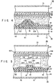
- FIGURE 4 is a cross-sectional view of the active matrix type liquid crystal display, taken on line A-A' of FIGURE 1.
- FIGURE 5 shows a cross-sectional view of the active matrix type liquid crystal display, taken on line B-B' of FIGURE 1.
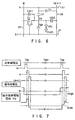
- FIGURE 6 indicates the equivalent circuit of each pixel of the active matrix type liquid crystal display shown in FIGURE 1.
- FIGURE 7 is a timing chart of one example of the driving wave form of the active matrix type liquid crystal display of this invention.
- FIGURE 8 shows a electrical characteristics of the active matrix type liquid crystal display of this invention.
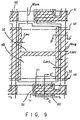
- FIGURE 9 is a plan view of a pixel area of an active matrix type liquid crystal display of the second embodiment of this invention.
- FIGURE 10 shows a play view of a pixel area of an active matrix type liquid crystal display of the third embodiment of this invention.
- FIGURE 11 is a cross-sectional view of the active matrix type liquid crystal display, taken on line E-E' of FIGURE 10.
- FIGURE 12 shows a cross-sectional view of the active matrix type liquid crystal display, taken on line F-F' of FIGURE 10.
- FIGURE 13 shows an example of the chart of the manufacturing process of the active matrix type liquid crystal display of this invention.
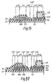
- FIGURE 14 is a plan view of a pixel area of an active matrix type liquid crystal display of an example compared with this invention.
- FIGURE 15 is a cross-sectional view of the active matrix type liquid crystal display, taken on line G-G' of FIGURE 14.
- FIGURE 16 is a plan view of a pixel area of an active matrix type liquid crystal display of another example compared with this invention.
- FIGURE 17 is a cross-sectional view of the active matrix type liquid crystal display, taken on line I-I' of FIGURE 19.
- FIGURE 18 is a plan view of a pixel area of an active matrix type liquid crystal display of a fourth embodiment of the present invention.
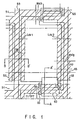
- FIG. 1 shows a plan view of a pixel area of a LCD of the first embodiment of this invention.
- FIG. 2 shows a plan view of the counter substrate of the LCD.
- FIG. 3 shows a plan view which indicates the effective display area of the LCD.
- FIG. 4 shows a cross-sectional view of the LCD, taken on line A-A' of FIG. 1.
- FIG. 5 shows a cross-sectional view of the LCD, taken on line B-B' of FIG. 1 and FIG. 3.
- an array substrate 63 has scanning lines 51 and signal lines 59 disposed on a transparent substrate 50 and crossing each other with a gate insulator 53 interposed therebetween.
- the width Wscn of the scanning line 51 is 14 ⁇ m
- the width Wsig of the signal line 59 is 5 ⁇ m, for example.
- the pixel electrode 58 is disposed on the area sectioned by the scanning line 51 and the signal line 59.
- the distance Lsp1 between the signal line 59 and the pixel electrode 58 is 3 ⁇ m, for example.
- the TFT 71 serves as a switching element which drives and controls the pixel electrode 58, and disposed on the scanning line 51.
- a gate electrode 54 of the TFT 71 is composed of a portion of the scanning line 51
- a semiconductor layer 55 is disposed on the gate electrode 54 with the gate insulator 53 interposed therebetween
- a source electrode 61 and a drain electrode 60 are disposed on the semiconductor layer 55 with passivation insulator 56 therebetween
- the drain electrode 60 is composed of a portion of the signal line 59.
- the channel region of the TFT 71 is disposed so as to be contained in the outline of the scanning line 51.
- the length L of the channel region is indicated as a minimum distance between the contact region of the source electrode 61 and the semiconductor layer 55 and the contact region of the drain electrode 60 and the semiconductor layer 55, and is 12 ⁇ m, in this embodiment.
- the width W of the channel region is indicated as the distance between the edge of the source electrode 61 and the drain electrode, and the width W is 30 ⁇ m.
- the scanning line 51 is elongated under the signal line 59.with the gate insulating layer 53 and the semiconductor layer 55 interposed therebetween, and this elongated portion of the scanning line 51 composes an elongated electrode 52.
- the elongated electrode 52 is disposed so as to shield the gap of the two pixel electrodes 58 neighboring each other, and the width of the electrode 52 is 19 ⁇ m.
- the elongated electrode 52 and the neighboring pixel electrodes 58 are overlapped together having the width Lov1 about 4 ⁇ m.
- each of the elongated electrodes 52 is overlapped with the side edge of the pixel electrode 58, and each of the electrodes 52 has an overlapped portion equal to the length of the pixel electrode 58.
- a counter substrate 68 has a shading layer 65 disposed on a transparent substrate 50 and extending along the scanning line 51, having the width of 40 ⁇ m, and color inking layer 66 of R (red), G (green), B (blue) extending to the cross direction with the shading layer 65, having the width of 97 ⁇ m.
- the distance Lsp2 between the neighboring two color layer 66 is 3 ⁇ m.
- the counter substrate 68 has a counter electrode 67 disposed on the color layer 66 and an orientation layer 70 covering the counter electrode 67.
- the aperture of one pixel is regulated at the area surrounded by the shading layer 65, the elongated electrode 52 and the signal line 59.
- the manufacturing method of the above-mentioned AM-LCD is demonstrated.
- the scanning line 51, the gate electrode which is a part of the scanning line 51 and the elongated electrode 52 are formed by carrying out photo etching process after carrying out the deposition of Ta film on the principal plane of the transparent substrate 50 which consists of glass, by 3000 angstrom thickness using the sputtering method.
- the gate insulating layer 53 is formed on the whole surface by carrying out the deposition of SiOx film to 3500 angstrom thickness using the plasma CVD method, so that it cover these electrodes subsequently.
- i-type hydrogenated amorphous silicon (a-Si) layer by 500 angstrom and SiNx layer by 2000 angstrom are formed in plasma CVD method one by one.
- this SiNx layer is photo-etched as the predetermined configuration, and the passivation insulator 56 is formed. Furthermore, on this, 500 angstrom of n-type a-Si layer is formed using plasma CVD method, and photo etching process of this n-type a-Si layer and the i-type a-Si layer is carried out at the predetermined configuration, and semiconductor layer 55 and ohmic layer 57a and 57b are formed.
- next 1000 angstrom deposition with the sputtering method, and photo etching process of ITO film is carried out at the predetermined configuration, and the pixel electrode 58 are formed.
- Mo film by 700 angstrom and A1 film by 3500 angstrom are deposited using sputtering method, and photo etching process of these films is carried out at the predetermined configuration, so as to form the signal line 59, the drain electrode 60 and the source electrode 61.
- the part of the n-type a-Si layer between the drain electrode 60 and the source electrode 61 is eliminated, with photo-resist on these left.
- the array substrate 63 is obtained by forming on the whole surface passivation layer of SiNx film at last, using plasma CVD method.
- Cr film is deposited by 1000 angstrom on the principal plane of the transparent substrate 64 which consists of glass, using sputtering method and this film is photo etched to the predetermined configuration to form the shading layer 65.
- the color inking layer 66 of R, G, B are formed at the region which is surrounded by the shading layer 65.
- This color inking layer 66 may be obtained by photo-etching a layer of photo-resist with pigment dispersed therein at the predetermined region. Also it may be obtained by transcribe the layer of binder resin with the pigment dispersed therein. In this embodiment, each color inking layer 66 is obtained by attaching a layer of 1.2 ⁇ m with pigment dispersed therein and photo etching this layer. Subsequently, the counter electrode 65 of ITO film is formed by 1500 angstrom using sputtering method, and the counter substrate 68 is obtained.
- the orientation layer 69 and 70 are disposed on the electrode formation side of the array substrate 63 and the counter substrate 68, by printing the low-temperature cure type polyimid film and rubbing these layer to give the orientation of the direction of predetermined.
- liquid crystal cell is obtained by combining the array substrate 63 and the counter substrate 68 so that the orientation axis of these substrates are crossed at the angle of 90 degree.
- FIG. 6 shows the equivalent circuit of each pixel of the AM-LCD.
- This equivalent circuit includes a storage capacitor Cs composed of the capacity coupling of the pixel electrode 58 and the elongated electrode 52, the capacitor Cds1 and Cds2 composed of the capacity coupling of the pixel electrode 58 and two signal lines 59 which is neighboring the pixel electrode 58, the capacitor Cgs composed of the capacity coupling of the gate electrode 54 and the source electrode 61, a liquid crystal capacitor Clc composed of the capacity coupling of the pixel electrode 58 and the counter electrode 67 through the liquid crystal layer 72, and a capacitor Cx composed of the capacity coupling which is mainly yielded at the overlapping portion of the elongated electrode 52 and the signal line 59.
- FIG. 7 indicates a example of timing chart of the driving wave form in this case of the operation.
- the liquid crystal display supply "active" voltage to one of the scanning line from the upper column of the matrix array and "non-active" voltage to the other scanning lines.
- Ton which is equal to a horizontal scanning interval of images which changes each frame interval
- Toff which is equal to a interval form the time cutting off the active voltage to the time supplying the active voltage again.
- this liquid crystal display supply image signal, according to one column line in a horizontal scanning cycle, to the signal line 59.
- the polarity of the image signal is inverted from the reference voltage Vsigc every predetermined cycle, for example every frame cycle.
- the active voltage Vg,on is considered as 25 V
- the reference voltage Vsigc is established as 7 V
- the signal voltage Vsig is inverted by the amplitude of 5 V from the voltage Vsigc, actually Vsig is established from the maximum amplitude 1 V of the negative side to the maximum amplitude 12 V of the positive side.
- the voltage Vp of the pixel electrode 58 is changed to the signal line voltage at the interval Ton, and held at the interval Toff.
- the pixel electrode 58 is capacity coupled with the elongated electrode 52 to make the storage capacitor Cs, so it is able to prevent the significant change of the voltage Vp in the interval Toff.
- And display is performed by optical transmission of liquid crystal layer 71 varying according to electric potential difference of the voltage Vcom of the counter electrode 67 and the voltage Vp of the pixel electrode 58.
- the voltage Vcom is established as 6 V in this case of the operation.
- the aperture ratio of the AM-LCD is resultly 70 % and therefore the utilization effectiveness of transmitted light from the light source rises, and electric power consumption can be reduced significantly.
- high grade display image is obtained owing to shading the interposed region between the pixel electrodes 58 neighboring mutually.
- the voltage of the pixel electrode 58 changes according to the change of the voltage of the signal line 59 at a horizontal scanning interval. Because of the dependency of the change of signal line 59 voltage on the image information, it is difficult to compensate the change of the voltage of the pixel electrode 58 uniformly. Contrary to this, the voltage of the scanning line 51 is fixed to the non-active voltage at the holding interval, and the change of the voltage of the pixel electrode 58 according to the scanning line 51 is substantially definite, so it is able to compensate the change of the voltage of the pixel electrode 58 using appropriate counter electrode voltage, for example.
- the elongated electrode 52 is disposed along the parallel portion between the signal line 59 and the pixel electrode 58, and the overlapped portion is disposed, by the predetermined length, between the elongated electrode 52 and the signal line 59 and between the elongated electrode 52 and the pixel electrode 58.
- the electric shield effect of the elongated electrode 52 which shield the pixel electrode 58 from signal line 59 is gained. Accordingly, it is able to reduce the change of the pixel electrode voltage, and approach the pixel electrode 58 to the signal electrode 59.
- the coupling capacitance between the scanning line 51 and the counter electrode 67 might be increased owing to the setting up the elongated electrode 52. If the capacitance is gained too much, the CR product of the scanning line 51 is increased, and accordingly the distortion of the active pulse is occurred. This distortion is increased according to the distance from the supplying point of the active pulse. On account of this, irregular voltage might be impressed to the pixel electrode 58 because of the turned on interval of the TFT is shortened or the irregular action of the TFT.
- the elongated electrode 52 of this embodiment is interposed between the substrate 50 and gate insulating layer 53 and disposed on the predetermined region corresponding to the pixel electrode 58 and the signal electrode 59, that is, the elongated electrode 52 is disposed so as to being apart from the counter electrode 67.
- the capacitance between the elongated 52 and the counter electrode 67 is established as a serial capacitance of the liquid crystal capacitance and the capacitance of the gate insulating layer, and it is able to reduce the coupling capacitance between the counter electrode 67 and the scanning line 51 and between the counter electrode 67 and the elongated electrode 52.
- the relative dielectric constant of the gate insulating layer 53 is about 4 and the constant of the liquid crystal layer is about 3.5 to 8 in this embodiment.
- the capacitance between the scanning line 51 or elongated electrode 52 and the counter electrode 67 is decreased by 10 % in comparison to the LCD which has no effective insulator such as gate insulating layer between its liquid crystal layer and its elongated electrode or its scanning line. This effect is extremely significant.
- the structure of this embodiment it is able to drive the large scale AM-LCD, which has more than 1920 signal lines and the capacitance belonging to the scanning electrode is risen accordingly.
- the voltage applied on the counter electrode 67 is distortioned when the capacitance and the CR product belonging to the counter electrode is risen too much. Accordingly, the liquid crystal capacitor is not charged up to the predetermined level and the uniformity of the image might be spoiled.
- the capacitance between the scanning line or the elongated electrode and the counter electrode can be reduced in the embodiment of this invention, above-mentioned uniformity is improved. Especially it is effective when the interval of alternating the driving signals is established such as a horizontal scanning interval.
- the elongated electrode 52 and the scanning line 51 are in one piece, so the space can be reduced which is necessary in the case that an independent main electrode is employed which supply voltage to the elongated electrode 52 and is disposed separately from the scanning line.
- the elongated electrode 52 is disposed so that it shades the region between the signal electrode 59 and the pixel electrode, so the area of the shading means is reduced and the aperture ratio of each pixel is gained sharply.
- the AM-LCD according to this embodiment can shade the tilt-reverse along the signal line completely and realize high performance.
- Tilt-reverse phenomenon is owing to the irregular alignment of the liquid crystal material along the electric field between the pixel electrode and the signal line at the peripheral portion of the pixel area to incur the undesirable light passage through the boundary between this irregular alignment region and the regular alignment region.
- this tilt-reverse domain is shaded completely by the adjustment of the width of the overlapping portion between the pixel electrode and the elongated electrode 52.
- the elongated electrode 52 is established substantially as the non-active voltage, that is, 0 V, and the pixel electrode 58 is established as the signal voltage by amplitude as 3 V to 5 V from the center voltage 6 V.
- the liquid crystal layer 71 disposed on the inner pixel area (effective display area) surrounded by the elongated electrode 52 is controlled directly by the electric field between the pixel electrode 58 and the counter electrode 67, and is aligned toward the original direction. Namely, the liquid crystal layer 71 at the effective display area is not effected directly by the electric field from the elongated electrode 52, so it is avoided that another tilt-reverse is generated within the effective display area.
- the tilt-reverse domain generated between the signal line 59 and the pixel electrode 58 can be shaded without another independent shading means, the elongated electrode 52 contributes to gaining the aperture ratio. In this embodiment, tilt-reverse domain along the signal line is not observed.
- the width of the elongated electrode 52 is established so as to be able to shade tilt-reverse domain.
- the width of the scanning line 51 may be established as the same width of the elongated electrode 52, but it is suitable to set the width of the elongated electrode 52 narrower than the scanning electrode 51.
- the operation speed of the TFT 71 is gained in proportion with the shortening the length of the channel region of the TFT 71 which is disposed on the scanning line 51.
- the capacitor Cx acts as a MOS capacitor.
- TEG Transmission Elementary Group 1 1 which includes a capacitor having the same structure as above-mentioned capacitor, is made through the same producing process as the element in the display area of the AM-LCD, and the capacitance is investigated by applying predetermined voltage.
- FIG. 8 shows the result of above investigation.
- the vertical axis indicates the value which normalize the investigated capacitance value C by the value Cox which indicates the capacitance of the capacitor having only gate insulating layer as its dielectric layer, and the horizontal axis indicates the applied voltage.
- the broken line shows the result of the investigation of TEG 1.
- the amplitude of the capacitance change of TEG 1 is 0.04 as long as the applied voltage is established between the range of 15 V and -15 V. This range is considered as actual range which applied on the capacitor disposed on the peripheral portion of each pixel area under general operation.
- the amplitude of the capacitance change of the parasitic capacitor Cx is minimized. So the level shift voltage ⁇ Vp can be compensated by adjusting the capacitance of Cs between the elongated electrode 52 and the pixel electrode 58. Accordingly, unevenness of the image is eliminated in this embodiment.
- the amplitude of the capacitance change of TEG 2 reaches about 0.33. Further the observation is carried out by operating this AM-LCD under above driving method. As a result, unevenness of the images is occurred.
- the AM-LCD which employs the structure of this embodiment has no short-circuit defect between the signal line 59 and the elongated electrode 52.
- the Nth column scanning line 51 and the elongated electrode 52 are disposed in one piece.
- This elongated electrode 52 is electrically coupled with the (N+1)th column pixel electrode 58 to make a capacitor Cs.
- the voltage of pixel electrode 58 is changed at the timing the active voltage is applied on the Nth column scanning line.
- the active voltage is applied on the (N+1)th column pixel electrode 58 and the signal voltage of the signal line 59 is transmitted to the (N+1)th column pixel electrode 58.
- the voltage of the Nth elongated electrode 52 is held within the holding interval. So the interval of holding the original voltage of the pixel electrode 58 is substantially equal to the holding interval.
- the channel region of the TFT 71 is formed within the outline of the scanning line. This formation of the channel region does not limit the formation of the elongated electrode 52, and contributes to gaining the aperture ratio of the AM-LCD.
- two elongated electrode 52 are formed at each side of the pixel electrode 58, and these electrodes have the overlapping portions with the signal line 59 and the pixel electrode 58 of substantially equal length each other. Accordingly, although the positioning of the elongated electrode 52 in concerning with the pixel electrode may be shifted from predetermined position along its length direction, the capacitance of the pixel electrode 58 coupled with the both side of the signal electrodes 59 is as substantially constant value. This structure is suitable while so called “ V-line inversion driving method " is carried out.
- This V-line inversion driving method is that the applied voltage on the neighboring signal lines are inverted with each other concerning with the center voltage of the signal line, and following effect is obtained by carrying out this method. Namely, the pixel electrode voltage is changed in accordance with the change of the signal voltage because of the electrically coupling between these electrodes, but as long as using this method, if the pixel electrode voltage is changed toward the positive side in accordance with the signal electrode disposed in one side of the pixel electrode, the other signal electrode disposed in the other side of the pixel electrode pulls down the pixel electrode voltage to the negative side.
- the change of the pixel electrode voltage is substantially canceled.
- the capacitors formed at both sides of the pixel electrode is not balanced, this cancel effect is spoiled.
- the length of the overlapping portions between the elongated electrode and the signal line or the pixel electrode formed at both side of the pixel electrode are established as substantially equal, resultly the capacitance formed surrounding the pixel electrode are balanced and above cancel effect is not spoiled.
- the storage capacitor Cs may be formed by overlapping the pixel electrode 58 and the elongated electrode 52 with the gate insulating layer interposed therebetween simply, on the other hand the interlayer composed of the gate insulating layer 53 and the semiconductor layer 55 is interposed between the elongated electrode 52 and the signal electrode 59. Accordingly, the capacitance Cs can be established as required value, on the other hand the capacitance of Cx can be reduced.
- FIG. 9 shows the second embodiment of this invention.
- the elongated electrode 52 may be blanched from the independent supply line.
- the aperture ratio is decreased a bit, however the applied voltage on the capacitor Cs can be established at any value so that the freedom of establishing the operating condition is obtained.
- the voltage of the elongated electrode 52 is established as the same voltage as the counter electrode 68.
- the aperture ratio is at 60 % and unevenness of the display is reduced in this embodiment.
- the semiconductor layer 55 formed on the elongated electrode 52 may be substantially aligned with the elongated electrode 52.
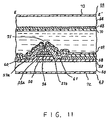
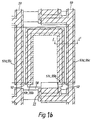
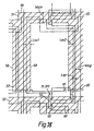
- FIG. 10 indicates the plane view of a pixel region of the AM-LCD of the third embodiment.
- FIG. 11 shows a cross-sectional view, taken in line E-E' shown in FIG. 10
- FIG. 12 shows a cross-sectional view, taken in line F-F' indicated in FIG. 10.
- the fundamental structure of the AM-LCD in this embodiment is substantially the same as the LCD shown in FIG. 1.
- the scanning line 51, the gate electrode which is a part of the scanning line 51 and the elongated electrode 52 are formed by carrying out photo-etching process after carrying out the deposition of Ta film on the principal plane of the transparent substrate 50 which consists of glass by 3000 angstrom thickness using the sputtering method.
- the gate insulating layer 53 is formed on the whole surface by carrying out the deposition of SiOx film to 3500 angstrom thickness using the plasma CVD method, so that it cover these electrodes subsequently.
- i-type a-Si layer by 500 angstrom and SiNx layer by 2000 angstrom are formed in plasma CVD method one by one.
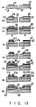
- this SiNx layer is photo-etched as the predetermined configuration, and the passivation insulator 56 is formed as shown in FIG. 13(b). Furthermore, on this, 700 angstrom of n-type a-Si layer is formed using plasma CVD method, and subsequently positive type photo-resist 85 is formed over the whole surface, then the surface including the photo-resist 85 is exposed from the side of the substrate applied no resist, as shown in FIG. 13(c).
- n-type a-Si 57 layer and i-type a-Si layer 55 extend from the portion covered by the photo-resist 85 are eliminated using photo-etching process, resultly these layer 55 and 57 are self-aligned with the gate electrode 54 and the elongated electrode 52, as shown in FIG. 13(d).
- Mo film by 700 angstrom and A1 film by 3500 angstrom are deposited using sputtering method, and photo-etching process of these films is carried out at the predetermined configuration, so as to form the signal line 59, the drain electrode 60 and the source electrode 61.
- the array substrate 63 is obtained by forming on the whole surface passivation layer of SiNx film at last, using plasma CVD method.
- AM-LCD is obtained by following manufacturing method as same as the first embodiment.
- the width Wscn of the scanning line 51 is as 14 ⁇ m
- the width of the signal line 59 is as 5 ⁇ m
- the distance Lsp2 between the signal line 59 and the pixel electrode 58 is as 4 ⁇ m
- the overlapping length Lov of the pixel electrode 58 and the elongated electrode 52 is as 4 ⁇ m.
- the width Ls2 of the elongated electrode 52 is established as 21 ⁇ m.
- FIG. 15 is the cross-sectional view, taken in line G-G' in FIG. 15.
- the semiconductor layer 55b, 55c and the ohmic layer 57c, 57d are not self-aligned with the elongated electrode 52, and formed by usual photo-etching method. Therefore the positioning margin Lm1 is required. And in the step of forming the pixel electrode 58, the margin Lm2 is required while positioning this electrode 58 on the semiconductor layer 55b as the same.
- the margin LM1, LM2 and LM3 are established as 3 ⁇ m and the distance Lsp1 is as 4 ⁇ m, for instance.
- the width Ls1 is as 39 ⁇ m.
- the width of the elongated electrode 52 is about 1/2 in above embodiment, therefore it is understood that the aperture ratio can improve sharply. Moreover, the short-circuit is not occurred at all.
- a further LCD in accordance with the invention is manufactured as shown in FIG. 16 and FIG. 17.
- the insulating layer formed on the elongated electrode is not self-aligned with the elongated electrode, and formed by usual photo-etching method. Therefore, in the step of forming the semiconductor layer 55b, positioning margin (Lm1 + Lm2) is required, and in the step of forming the insulating layer 56b, positioning margin Lm1 and Lm4 is required while positioning this layer on the semiconductor layer 55b.
- the margin Lm1, Lm2, Lm3, Lm4, Lm5 and Lm6 are established as 3 ⁇ m, therefore the width Ls1 is as 55 ⁇ m.
- the width of the elongated electrode 52 is about 1/3 in above embodiment, therefore it is understood that the aperture ratio can improve sharply, moreover the short-circuit not occur at all.
- the pixel electrodes neighboring each other are connected by the a-Si layer in this embodiment. Since this a-Si layer serves as a variable resistor, short-circuiting could occur between these pixel electrodes while electric current leakage is generated in the a-Si layer.
- the leakage between the neighboroing pixel electrodes is sufficiently reduced satisfactory under usual operation. That is considered because the a-Si layer is formed thin enough to reduce the photo-carrier in the same. Therefore the step of separating this a-Si layer into some island configuration can be omitted.
- the aperture ratio can improve sharply, moreover the short-circuit does not occur at all.
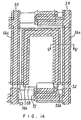
- FIG. 18 shows a fourth embodiment of this invention.
- the configuration of the shading layer 65 formed on the counter substrate 68 is modified. That is, the elongated electrode 52 is extended beyond the edge of the source electrode to the neighborhood of the scanning electrode 51 of next column, and the shading layer 65 is formed so as to cross the elongated electrode 52 and the source electrode 61.
- This structure can reduce the shading area between the scanning electrode 51 and the pixel electrode 58 by using the source electrode 61 as a shading means, and improve the aperture ratio still more.
- an optical black stripe layer may be formed on the signal electrode 59 directly, with any layer inserted therebetween, or formed on the portion of the counter substrate faced to the signal electrode 59.
- the contrast can be improved sharply by sectioning the neighboring pixel area. While the width of the stripe layer is established as less than or equal to the width of the elongated electrode 52, the contrast of display can be improved without reducing the aperture ratio.
- the stripe layer for instance, some metallic material or oxide material, such as Cr, can be applied. Or a resin layer with black pigment or metallic filler dispersed therein is also suitable. Moreover the stack of above material can be employed. Also it is suitable to overlap the neighboring color inking layer 66 each other at the portion of the counter substrate 68 faced to the signal electrode 59. By selecting anti-reflective material from above example, the reflection of outer ray can be reduced to obtain high contrast display.
Landscapes
- Physics & Mathematics (AREA)
- Nonlinear Science (AREA)
- Engineering & Computer Science (AREA)
- Microelectronics & Electronic Packaging (AREA)
- Mathematical Physics (AREA)
- Chemical & Material Sciences (AREA)
- Crystallography & Structural Chemistry (AREA)
- General Physics & Mathematics (AREA)
- Optics & Photonics (AREA)
- Power Engineering (AREA)
- Liquid Crystal (AREA)
- Thin Film Transistor (AREA)
Description
- The present invention relates to an active matrix type display having a pixel electrodes array which employs thin film transistor (TFT) as a switching element, and a method of manufacturing same.
- The conventional active matrix type liquid crystal displays (AM-LCDs) have a liquid crystal element interposed between an array substrate and a counter substrate.
- The array substrate includes a matrix array of pixel electrodes disposed on a transparent substrate such as a glass substrate, scanning lines disposed along the column of these pixel electrodes array, signal lines disposed along the row electrodes the pixel electrodes array, TFTs which control the pixel electrodes in response to the voltage signal applied to the scanning lines and the signal lines, and storage capacitor electrodes electrically connected to the pixel electrode through an insulating layer.
- The counter substrate includes a counter electrode disposed on a transparent substrate such as a glass substrate and confronted with the matrix array of the pixel electrodes, and a black matrix which shield between the pixel electrodes. When the AM-LCD is used in a color display system, a color inking layer is disposed on the area surrounded by the black matrix and faced to the pixel electrodes.
- The liquid crystal display supply "active" voltage to one of the scanning line from the upper column of the matrix array and "non-active" voltage to the other scanning lines. When each TFT is turned on through a switching interval, the TFT transmits the voltage applied on the signal line to the pixel electrode. And when each TFT is turned off through a holding interval, the voltage transmitted to the pixel electrode is held by the pixel capacitor composed between the pixel electrode and the counter electrode, and the storage capacitor composed between the pixel electrode and the storage electrode.
- The holding interval is equal to the interval from the time cutting off the active voltage to the time supplying the same again. The transparency of the liquid crystal layer is changed according to the voltage between the pixel electrode and the counter electrode. The LCD displays the image by controlling the distribution of the transparency of the liquid crystal layer and modifying the light from a backlight source.
- The aperture ratio of each pixel is indicated as a ratio of the transparent area to the whole pixel area. In the conventional LCDs, the aperture ratio is generally 30% to 40%. Accordingly, it is difficult to gain the required brightness. As a countermeasure to this problem, it is considered to increase the light intensity of the light source, but this measure has a shortcoming that it increases power consumption.
- It is considered to decrease the area of a driving circuit of each pixel as another measure, but makes it difficult to maintain the yield on the production.
- An example of an active matrix device is disclosed in JP 5 203 9994 A or EP 0592 063 A published after the priority of the present application.
- It is therefore an object of the present invention to provide an active matrix type display which is suitable for a high performance display device and for high productivity.
- Accordingly the present invention provides an active matrix type display device comprising:
- a plurality of scanning lines disposed on an insulating substrate;
- a plurality of signal lines crossing the scanning lines;
- a gate insulating layer interposed between the scanning lines and the signal lines;
- a plurality of thin film transistors having a semiconductor layer disposed on the gate insulating layer and a passivation layer disposed on the semiconductor layer,
- a plurality of capacity actuation type pixels disposed by the crossing point of the scanning line and the signal line, wherein each pixel has a pixel electrode which is electrically coupled with the signal line through the thin film transistor; and
- a plurality of storage capacitors each having a first electrode as a part of one of the pixel electrodes; further comprising a plurality of elongated electrodes respectively disposed along and under each signal line, wherein each elongated electrode is wider than the signal electrode and has an overlap portion therewith through a dielectric layer composed of the same layer as the gate insulating layer and the semiconductor layer; whereby a part of the elongated electrode serves as a second electrode of the storage capacitor, characterised in that the semiconductor layer is comprised of part of the semiconductor layer of the thin film transistor and extends along the signal line, the semiconductor layer being interposed between the opposing edges of adjacent pixel electrodes, respectively, and the channel region of the thin film transistor being formed on the scanning line within the outlines of the scanning line.
-
- The advantages offered by the invention are mainly that the elongated electrode serves as an electric shield between the signal line and the pixel electrode, so that the parasitic capacitor between these electrode is reduced sharply. As a result, the distance between these electrode is also reduced to improve the aperture ratio of the active matrix type display device.
- While the semiconductor layer and the gate insulating layer is interposed between the signal line and the elongated electrode, short-circuit defect is reduced sharply, moreover the semiconductor layer is thinner enough to reduce the changeability of the parasitic capacitor formed between the elongated electrode and the signal line.
- FIGURE 1 is a plan view of a pixel area of an active matrix type liquid crystal display of the present invention.
- FIGURE 2 is a plan view of the counter substrate of the active matrix type liquid crystal display shown in FIGURE 1.
- FIGURE 3 is a plan view which indicates the effective display area of the active matrix type liquid crystal display shown in FIGURE 1.
- FIGURE 4 is a cross-sectional view of the active matrix type liquid crystal display, taken on line A-A' of FIGURE 1.
- FIGURE 5 shows a cross-sectional view of the active matrix type liquid crystal display, taken on line B-B' of FIGURE 1.
- FIGURE 6 indicates the equivalent circuit of each pixel of the active matrix type liquid crystal display shown in FIGURE 1.
- FIGURE 7 is a timing chart of one example of the driving wave form of the active matrix type liquid crystal display of this invention.
- FIGURE 8 shows a electrical characteristics of the active matrix type liquid crystal display of this invention.
- FIGURE 9 is a plan view of a pixel area of an active matrix type liquid crystal display of the second embodiment of this invention.
- FIGURE 10 shows a play view of a pixel area of an active matrix type liquid crystal display of the third embodiment of this invention.
- FIGURE 11 is a cross-sectional view of the active matrix type liquid crystal display, taken on line E-E' of FIGURE 10.
- FIGURE 12 shows a cross-sectional view of the active matrix type liquid crystal display, taken on line F-F' of FIGURE 10.
- FIGURE 13 shows an example of the chart of the manufacturing process of the active matrix type liquid crystal display of this invention.
- FIGURE 14 is a plan view of a pixel area of an active matrix type liquid crystal display of an example compared with this invention.
- FIGURE 15 is a cross-sectional view of the active matrix type liquid crystal display, taken on line G-G' of FIGURE 14.
- FIGURE 16 is a plan view of a pixel area of an active matrix type liquid crystal display of another example compared with this invention.
- FIGURE 17 is a cross-sectional view of the active matrix type liquid crystal display, taken on line I-I' of FIGURE 19.
- FIGURE 18 is a plan view of a pixel area of an active matrix type liquid crystal display of a fourth embodiment of the present invention.
- FIG. 1 shows a plan view of a pixel area of a LCD of the first embodiment of this invention. FIG. 2 shows a plan view of the counter substrate of the LCD. FIG. 3 shows a plan view which indicates the effective display area of the LCD. FIG. 4 shows a cross-sectional view of the LCD, taken on line A-A' of FIG. 1. FIG. 5 shows a cross-sectional view of the LCD, taken on line B-B' of FIG. 1 and FIG. 3.
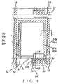
- As shown in FIG. 1, FIG. 4 and FIG. 5, an
array substrate 63 hasscanning lines 51 andsignal lines 59 disposed on atransparent substrate 50 and crossing each other with agate insulator 53 interposed therebetween. The width Wscn of thescanning line 51 is 14 µm, and the width Wsig of thesignal line 59 is 5 µm, for example. - The
pixel electrode 58 is disposed on the area sectioned by thescanning line 51 and thesignal line 59. The distance Lsp1 between thesignal line 59 and thepixel electrode 58 is 3 µm, for example. - The TFT 71 serves as a switching element which drives and controls the
pixel electrode 58, and disposed on thescanning line 51. Namely, agate electrode 54 of theTFT 71 is composed of a portion of thescanning line 51, asemiconductor layer 55 is disposed on thegate electrode 54 with thegate insulator 53 interposed therebetween, asource electrode 61 and adrain electrode 60 are disposed on thesemiconductor layer 55 withpassivation insulator 56 therebetween, and thedrain electrode 60 is composed of a portion of thesignal line 59. - The channel region of the TFT 71 is disposed so as to be contained in the outline of the
scanning line 51. The length L of the channel region is indicated as a minimum distance between the contact region of thesource electrode 61 and thesemiconductor layer 55 and the contact region of thedrain electrode 60 and thesemiconductor layer 55, and is 12 µ m, in this embodiment. And the width W of the channel region is indicated as the distance between the edge of thesource electrode 61 and the drain electrode, and the width W is 30 µ m. - The
scanning line 51 is elongated under the signal line 59.with thegate insulating layer 53 and thesemiconductor layer 55 interposed therebetween, and this elongated portion of thescanning line 51 composes anelongated electrode 52. Theelongated electrode 52 is disposed so as to shield the gap of the twopixel electrodes 58 neighboring each other, and the width of theelectrode 52 is 19 µm. Theelongated electrode 52 and the neighboringpixel electrodes 58 are overlapped together having the width Lov1 about 4 µm. And each of theelongated electrodes 52 is overlapped with the side edge of thepixel electrode 58, and each of theelectrodes 52 has an overlapped portion equal to the length of thepixel electrode 58. - As shown in FIG. 2 and FIG. 4, a
counter substrate 68 has ashading layer 65 disposed on atransparent substrate 50 and extending along thescanning line 51, having the width of 40 µm, andcolor inking layer 66 of R (red), G (green), B (blue) extending to the cross direction with theshading layer 65, having the width of 97 µm. The distance Lsp2 between the neighboring twocolor layer 66 is 3 µm. Thecounter substrate 68 has acounter electrode 67 disposed on thecolor layer 66 and anorientation layer 70 covering thecounter electrode 67. - As shown in FIG. 3, the aperture of one pixel is regulated at the area surrounded by the
shading layer 65, theelongated electrode 52 and thesignal line 59. - Next, the manufacturing method of the above-mentioned AM-LCD is demonstrated. First, the
scanning line 51, the gate electrode which is a part of thescanning line 51 and theelongated electrode 52 are formed by carrying out photo etching process after carrying out the deposition of Ta film on the principal plane of thetransparent substrate 50 which consists of glass, by 3000 angstrom thickness using the sputtering method. - The
gate insulating layer 53 is formed on the whole surface by carrying out the deposition of SiOx film to 3500 angstrom thickness using the plasma CVD method, so that it cover these electrodes subsequently. - Next, i-type hydrogenated amorphous silicon (a-Si) layer by 500 angstrom and SiNx layer by 2000 angstrom are formed in plasma CVD method one by one.
- Subsequently this SiNx layer is photo-etched as the predetermined configuration, and the
passivation insulator 56 is formed. Furthermore, on this, 500 angstrom of n-type a-Si layer is formed using plasma CVD method, and photo etching process of this n-type a-Si layer and the i-type a-Si layer is carried out at the predetermined configuration, andsemiconductor layer 55 andohmic layer - Next 1000 angstrom deposition with the sputtering method, and photo etching process of ITO film is carried out at the predetermined configuration, and the
pixel electrode 58 are formed. And subsequently, Mo film by 700 angstrom and A1 film by 3500 angstrom are deposited using sputtering method, and photo etching process of these films is carried out at the predetermined configuration, so as to form thesignal line 59, thedrain electrode 60 and thesource electrode 61. And the part of the n-type a-Si layer between thedrain electrode 60 and thesource electrode 61 is eliminated, with photo-resist on these left. And thearray substrate 63 is obtained by forming on the whole surface passivation layer of SiNx film at last, using plasma CVD method. - On the other hand, Cr film is deposited by 1000 angstrom on the principal plane of the
transparent substrate 64 which consists of glass, using sputtering method and this film is photo etched to the predetermined configuration to form theshading layer 65. And thecolor inking layer 66 of R, G, B are formed at the region which is surrounded by theshading layer 65. - This
color inking layer 66 may be obtained by photo-etching a layer of photo-resist with pigment dispersed therein at the predetermined region. Also it may be obtained by transcribe the layer of binder resin with the pigment dispersed therein. In this embodiment, eachcolor inking layer 66 is obtained by attaching a layer of 1.2 µm with pigment dispersed therein and photo etching this layer. Subsequently, thecounter electrode 65 of ITO film is formed by 1500 angstrom using sputtering method, and thecounter substrate 68 is obtained. - Then, the
orientation layer array substrate 63 and thecounter substrate 68, by printing the low-temperature cure type polyimid film and rubbing these layer to give the orientation of the direction of predetermined. - And the liquid crystal cell is obtained by combining the
array substrate 63 and thecounter substrate 68 so that the orientation axis of these substrates are crossed at the angle of 90 degree. - At this time, positioning of the
array substrate 63 with thecounter substrate 68 is carried out using the alignment mark prepared in the predetermined location of thetransparent substrate polarization films 73 and 74 are stuck on the outer plane of thearray substrate 63 and thecounter substrate 68, and the AM-LCD of this embodiment is obtained. - Next, the example of an operation of the above-mentioned AM-LCD is demonstrated.
- FIG. 6 shows the equivalent circuit of each pixel of the AM-LCD. This equivalent circuit includes a storage capacitor Cs composed of the capacity coupling of the
pixel electrode 58 and theelongated electrode 52, the capacitor Cds1 and Cds2 composed of the capacity coupling of thepixel electrode 58 and twosignal lines 59 which is neighboring thepixel electrode 58, the capacitor Cgs composed of the capacity coupling of thegate electrode 54 and thesource electrode 61, a liquid crystal capacitor Clc composed of the capacity coupling of thepixel electrode 58 and thecounter electrode 67 through theliquid crystal layer 72, and a capacitor Cx composed of the capacity coupling which is mainly yielded at the overlapping portion of theelongated electrode 52 and thesignal line 59. - FIG. 7 indicates a example of timing chart of the driving wave form in this case of the operation. The liquid crystal display supply "active" voltage to one of the scanning line from the upper column of the matrix array and "non-active" voltage to the other scanning lines. At each
scanning line 51, the active voltage is maintained at the switching interval Ton which is equal to a horizontal scanning interval of images which changes each frame interval, and the non-active voltage is maintained at the holding interval Toff which is equal to a interval form the time cutting off the active voltage to the time supplying the active voltage again. - On the other hand, this liquid crystal display supply image signal, according to one column line in a horizontal scanning cycle, to the
signal line 59. The polarity of the image signal is inverted from the reference voltage Vsigc every predetermined cycle, for example every frame cycle. In this embodiment, the active voltage Vg,on is considered as 25 V, the non-active voltage Vg,off -2 V. And the reference voltage Vsigc is established as 7 V, and the signal voltage Vsig is inverted by the amplitude of 5 V from the voltage Vsigc, actually Vsig is established from the maximum amplitude 1 V of the negative side to the maximum amplitude 12 V of the positive side. - The voltage Vp of the
pixel electrode 58 is changed to the signal line voltage at the interval Ton, and held at the interval Toff. Thepixel electrode 58 is capacity coupled with theelongated electrode 52 to make the storage capacitor Cs, so it is able to prevent the significant change of the voltage Vp in the interval Toff. - And display is performed by optical transmission of
liquid crystal layer 71 varying according to electric potential difference of the voltage Vcom of thecounter electrode 67 and the voltage Vp of thepixel electrode 58. The voltage Vcom is established as 6 V in this case of the operation. - In this embodiment, the aperture ratio of the AM-LCD is resultly 70 % and therefore the utilization effectiveness of transmitted light from the light source rises, and electric power consumption can be reduced significantly. And high grade display image is obtained owing to shading the interposed region between the
pixel electrodes 58 neighboring mutually. - Namely, the voltage of the
pixel electrode 58 changes according to the change of the voltage of thesignal line 59 at a horizontal scanning interval. Because of the dependency of the change ofsignal line 59 voltage on the image information, it is difficult to compensate the change of the voltage of thepixel electrode 58 uniformly. Contrary to this, the voltage of thescanning line 51 is fixed to the non-active voltage at the holding interval, and the change of the voltage of thepixel electrode 58 according to thescanning line 51 is substantially definite, so it is able to compensate the change of the voltage of thepixel electrode 58 using appropriate counter electrode voltage, for example. - In this point of view, the
elongated electrode 52 is disposed along the parallel portion between thesignal line 59 and thepixel electrode 58, and the overlapped portion is disposed, by the predetermined length, between theelongated electrode 52 and thesignal line 59 and between theelongated electrode 52 and thepixel electrode 58. Employing this structure, the electric shield effect of theelongated electrode 52 which shield thepixel electrode 58 fromsignal line 59 is gained. Accordingly, it is able to reduce the change of the pixel electrode voltage, and approach thepixel electrode 58 to thesignal electrode 59. - Apart from that, the coupling capacitance between the scanning
line 51 and thecounter electrode 67 might be increased owing to the setting up theelongated electrode 52. If the capacitance is gained too much, the CR product of thescanning line 51 is increased, and accordingly the distortion of the active pulse is occurred. This distortion is increased according to the distance from the supplying point of the active pulse. On account of this, irregular voltage might be impressed to thepixel electrode 58 because of the turned on interval of the TFT is shortened or the irregular action of the TFT. - On the contrary, the
elongated electrode 52 of this embodiment is interposed between thesubstrate 50 andgate insulating layer 53 and disposed on the predetermined region corresponding to thepixel electrode 58 and thesignal electrode 59, that is, theelongated electrode 52 is disposed so as to being apart from thecounter electrode 67. In this case, the capacitance between the elongated 52 and thecounter electrode 67 is established as a serial capacitance of the liquid crystal capacitance and the capacitance of the gate insulating layer, and it is able to reduce the coupling capacitance between thecounter electrode 67 and thescanning line 51 and between thecounter electrode 67 and theelongated electrode 52. - The relative dielectric constant of the
gate insulating layer 53 is about 4 and the constant of the liquid crystal layer is about 3.5 to 8 in this embodiment. In this case, it is realized that the capacitance between the scanningline 51 orelongated electrode 52 and thecounter electrode 67 is decreased by 10 % in comparison to the LCD which has no effective insulator such as gate insulating layer between its liquid crystal layer and its elongated electrode or its scanning line. This effect is extremely significant. - According to use of the structure of this embodiment, it is able to drive the large scale AM-LCD, which has more than 1920 signal lines and the capacitance belonging to the scanning electrode is risen accordingly.
- Further, another driving method which employs the alternating wave form of the counter electrode voltage within the same cycle as the alternation of the signal electrode voltage is known. By using this method, the pressure of the signal line driver can be reduced and it is useful to reduce the manufacturing cost of the display device.
- In this case, however, the voltage applied on the
counter electrode 67 is distortioned when the capacitance and the CR product belonging to the counter electrode is risen too much. Accordingly, the liquid crystal capacitor is not charged up to the predetermined level and the uniformity of the image might be spoiled. - On the other hand, the capacitance between the scanning line or the elongated electrode and the counter electrode can be reduced in the embodiment of this invention, above-mentioned uniformity is improved. Especially it is effective when the interval of alternating the driving signals is established such as a horizontal scanning interval.
- Furthermore, the
elongated electrode 52 and thescanning line 51 are in one piece, so the space can be reduced which is necessary in the case that an independent main electrode is employed which supply voltage to theelongated electrode 52 and is disposed separately from the scanning line. And theelongated electrode 52 is disposed so that it shades the region between thesignal electrode 59 and the pixel electrode, so the area of the shading means is reduced and the aperture ratio of each pixel is gained sharply. - This effect of gaining the aperture ratio is explained in more details. In the field of AM-LCD, it is known that the liquid crystal material shows irregular alignment at the edge portion of the pixel region as a " tilt-reverse " phenomenon, the AM-LCD according to this embodiment can shade the tilt-reverse along the signal line completely and realize high performance. Tilt-reverse phenomenon is owing to the irregular alignment of the liquid crystal material along the electric field between the pixel electrode and the signal line at the peripheral portion of the pixel area to incur the undesirable light passage through the boundary between this irregular alignment region and the regular alignment region.
- In this embodiment, this tilt-reverse domain is shaded completely by the adjustment of the width of the overlapping portion between the pixel electrode and the
elongated electrode 52. - The
elongated electrode 52 is established substantially as the non-active voltage, that is, 0 V, and thepixel electrode 58 is established as the signal voltage by amplitude as 3 V to 5 V from the center voltage 6 V. - In this operation, the electric field between the
elongated electrode 52 and thepixel electrode 58 is generated, and it is considered that another tilt-reverse domain might occur along the electric field from theelongated electrode 52 through the region between thepixel electrode 58 and thesignal line 59. - However, as long as hiding the tilt-reverse domain near the
signal line 59, theliquid crystal layer 71 disposed on the inner pixel area (effective display area) surrounded by theelongated electrode 52 is controlled directly by the electric field between thepixel electrode 58 and thecounter electrode 67, and is aligned toward the original direction. Namely, theliquid crystal layer 71 at the effective display area is not effected directly by the electric field from theelongated electrode 52, so it is avoided that another tilt-reverse is generated within the effective display area. - Accordingly the tilt-reverse domain generated between the
signal line 59 and thepixel electrode 58 can be shaded without another independent shading means, theelongated electrode 52 contributes to gaining the aperture ratio. In this embodiment, tilt-reverse domain along the signal line is not observed. - According to the structure of this embodiment, the width of the
elongated electrode 52 is established so as to be able to shade tilt-reverse domain. The width of thescanning line 51 may be established as the same width of theelongated electrode 52, but it is suitable to set the width of theelongated electrode 52 narrower than thescanning electrode 51. - The operation speed of the
TFT 71 is gained in proportion with the shortening the length of the channel region of theTFT 71 which is disposed on thescanning line 51. - However, as long as shortening the length of the channel region without changing the width of the
scanning line 51, the overlapping area between thesource electrode 61 and thescanning line 51, and the capacitance between these electrode is also risen. The level shift voltage ΔVp is indicated as follows. - In this embodiment, the capacitor Cx acts as a MOS capacitor. In order to observe the specific of this capacitor, TEG (Test Elementary Group) 1, which includes a capacitor having the same structure as above-mentioned capacitor, is made through the same producing process as the element in the display area of the AM-LCD, and the capacitance is investigated by applying predetermined voltage.
- FIG. 8 shows the result of above investigation. The vertical axis indicates the value which normalize the investigated capacitance value C by the value Cox which indicates the capacitance of the capacitor having only gate insulating layer as its dielectric layer, and the horizontal axis indicates the applied voltage.
- And the broken line shows the result of the investigation of
TEG 1. As shown in FIG. 8, the amplitude of the capacitance change ofTEG 1 is 0.04 as long as the applied voltage is established between the range of 15 V and -15 V. This range is considered as actual range which applied on the capacitor disposed on the peripheral portion of each pixel area under general operation. - As shown above, the amplitude of the capacitance change of the parasitic capacitor Cx is minimized. So the level shift voltage Δ Vp can be compensated by adjusting the capacitance of Cs between the
elongated electrode 52 and thepixel electrode 58. Accordingly, unevenness of the image is eliminated in this embodiment. - In comparison to this, another AM-LCD is obtained without any passivation insulating layer on the channel region of its TFT and
TEG 2 which includes a capacitor having the same structure of its pixel area similarly, and the specific of the capacitor is investigated. The real line in FIG. 8 indicates the result of this investigation. The difference of manufacturing method of AM-LCD and the method of investigating the specific in comparison to above method is that the passivation layer is not formed on the channel region, and according to this, the thickness of its semiconductor layer is established as 3300 angstrom. - As shown in FIG. 8, the amplitude of the capacitance change of
TEG 2 reaches about 0.33. Further the observation is carried out by operating this AM-LCD under above driving method. As a result, unevenness of the images is occurred. - Furthermore, the AM-LCD which employs the structure of this embodiment has no short-circuit defect between the
signal line 59 and theelongated electrode 52. - In addition to this, the Nth
column scanning line 51 and theelongated electrode 52 are disposed in one piece. Thiselongated electrode 52 is electrically coupled with the (N+1)thcolumn pixel electrode 58 to make a capacitor Cs. The voltage ofpixel electrode 58 is changed at the timing the active voltage is applied on the Nth column scanning line. - After that, the active voltage is applied on the (N+1)th
column pixel electrode 58 and the signal voltage of thesignal line 59 is transmitted to the (N+1)thcolumn pixel electrode 58. The voltage of the Nth elongatedelectrode 52 is held within the holding interval. So the interval of holding the original voltage of thepixel electrode 58 is substantially equal to the holding interval. - As the transparency of the
liquid crystal layer 72 is changed in response with the effective value of the applied voltage, display images is scarcely effected by the change of the pixel electrode voltage according to the change of the elongated electrode voltage. - And the channel region of the
TFT 71 is formed within the outline of the scanning line. This formation of the channel region does not limit the formation of theelongated electrode 52, and contributes to gaining the aperture ratio of the AM-LCD. - Furthermore, two
elongated electrode 52 are formed at each side of thepixel electrode 58, and these electrodes have the overlapping portions with thesignal line 59 and thepixel electrode 58 of substantially equal length each other. Accordingly, although the positioning of theelongated electrode 52 in concerning with the pixel electrode may be shifted from predetermined position along its length direction, the capacitance of thepixel electrode 58 coupled with the both side of thesignal electrodes 59 is as substantially constant value. This structure is suitable while so called " V-line inversion driving method " is carried out. - This V-line inversion driving method is that the applied voltage on the neighboring signal lines are inverted with each other concerning with the center voltage of the signal line, and following effect is obtained by carrying out this method. Namely, the pixel electrode voltage is changed in accordance with the change of the signal voltage because of the electrically coupling between these electrodes, but as long as using this method, if the pixel electrode voltage is changed toward the positive side in accordance with the signal electrode disposed in one side of the pixel electrode, the other signal electrode disposed in the other side of the pixel electrode pulls down the pixel electrode voltage to the negative side.
- As a result, the change of the pixel electrode voltage is substantially canceled. However, if the capacitors formed at both sides of the pixel electrode is not balanced, this cancel effect is spoiled. Then, in the case of this embodiment, the length of the overlapping portions between the elongated electrode and the signal line or the pixel electrode formed at both side of the pixel electrode are established as substantially equal, resultly the capacitance formed surrounding the pixel electrode are balanced and above cancel effect is not spoiled.
- Accordingly high performance display is obtained with the fundamental structure of this embodiment which can reduce the capacitance between the
signal line 59 and thepixel electrode 58. - In this embodiment, it becomes able to obtain a LCD of high aperture ratio and high performance.
- It is able to modify above embodiment variously. For instance, the storage capacitor Cs may be formed by overlapping the
pixel electrode 58 and theelongated electrode 52 with the gate insulating layer interposed therebetween simply, on the other hand the interlayer composed of thegate insulating layer 53 and thesemiconductor layer 55 is interposed between theelongated electrode 52 and thesignal electrode 59. Accordingly, the capacitance Cs can be established as required value, on the other hand the capacitance of Cx can be reduced. - FIG. 9 shows the second embodiment of this invention. As shown in FIG. 9, the
elongated electrode 52 may be blanched from the independent supply line. In this case, the aperture ratio is decreased a bit, however the applied voltage on the capacitor Cs can be established at any value so that the freedom of establishing the operating condition is obtained. In this operation, the voltage of theelongated electrode 52 is established as the same voltage as thecounter electrode 68. The aperture ratio is at 60 % and unevenness of the display is reduced in this embodiment. - As shown in FIG. 10, the
semiconductor layer 55 formed on theelongated electrode 52 may be substantially aligned with theelongated electrode 52. - FIG. 10 indicates the plane view of a pixel region of the AM-LCD of the third embodiment. FIG. 11 shows a cross-sectional view, taken in line E-E' shown in FIG. 10, and FIG. 12 shows a cross-sectional view, taken in line F-F' indicated in FIG. 10. The fundamental structure of the AM-LCD in this embodiment is substantially the same as the LCD shown in FIG. 1.
- Next, the manufacturing method of the AM-LCD in this embodiment is demonstrated.
- As shown in FIG. 13 (a), the
scanning line 51, the gate electrode which is a part of thescanning line 51 and theelongated electrode 52 are formed by carrying out photo-etching process after carrying out the deposition of Ta film on the principal plane of thetransparent substrate 50 which consists of glass by 3000 angstrom thickness using the sputtering method. - The
gate insulating layer 53 is formed on the whole surface by carrying out the deposition of SiOx film to 3500 angstrom thickness using the plasma CVD method, so that it cover these electrodes subsequently. - Next, i-type a-Si layer by 500 angstrom and SiNx layer by 2000 angstrom are formed in plasma CVD method one by one.
- Subsequently this SiNx layer is photo-etched as the predetermined configuration, and the
passivation insulator 56 is formed as shown in FIG. 13(b). Furthermore, on this, 700 angstrom of n-type a-Si layer is formed using plasma CVD method, and subsequently positive type photo-resist 85 is formed over the whole surface, then the surface including the photo-resist 85 is exposed from the side of the substrate applied no resist, as shown in FIG. 13(c). And after the development of the resist 85, n-type a-Si 57 layer and i-type a-Si layer 55 extend from the portion covered by the photo-resist 85 are eliminated using photo-etching process, resultly theselayer gate electrode 54 and theelongated electrode 52, as shown in FIG. 13(d). - Next 1000 angstrom deposition with the sputtering method, and photo-etching process of ITO film is carried out at the predetermined configuration, and the
pixel electrode 58 are formed, as shown in FIG. 13(e). - And subsequently, Mo film by 700 angstrom and A1 film by 3500 angstrom are deposited using sputtering method, and photo-etching process of these films is carried out at the predetermined configuration, so as to form the
signal line 59, thedrain electrode 60 and thesource electrode 61. - And the part of the n-type a-Si layer and the i-type a-Si layer extending from the portion covered with these electrode and photo-resist left on these electrode to form the
semiconductor layer ohmic layer array substrate 63 is obtained by forming on the whole surface passivation layer of SiNx film at last, using plasma CVD method. - Then AM-LCD is obtained by following manufacturing method as same as the first embodiment.
- In this embodiment, the width Wscn of the
scanning line 51 is as 14 µm, and the width of thesignal line 59 is as 5 µm, and the distance Lsp2 between thesignal line 59 and thepixel electrode 58 is as 4 µm. And the overlapping length Lov of thepixel electrode 58 and theelongated electrode 52 is as 4 µm. In this case, the width Ls2 of theelongated electrode 52 is indicated as follows. - Accordingly, the width Ls2 of the
elongated electrode 52 is established as 21 µm. - In comparison to this, another LCD is manufactured as shown in FIG. 14 to compare the aperture ratio of LCD with above embodiment.
- FIG. 15 is the cross-sectional view, taken in line G-G' in FIG. 15. In this sample, the
semiconductor layer ohmic layer elongated electrode 52, and formed by usual photo-etching method. Therefore the positioning margin Lm1 is required. And in the step of forming thepixel electrode 58, the margin Lm2 is required while positioning thiselectrode 58 on thesemiconductor layer 55b as the same. - Subsequently, in the step of forming the
signal line 59, the margin Lm3 is required while positioning thiselectrode 59 on thesemiconductor layer 55c. Therefore, the width LS1 of theelongated electrode 52 is as follows. - The margin LM1, LM2 and LM3 are established as 3 µm and the distance Lsp1 is as 4 µm, for instance. In this case, the width Ls1 is as 39 µm. As compared with this, the width of the
elongated electrode 52 is about 1/2 in above embodiment, therefore it is understood that the aperture ratio can improve sharply. Moreover, the short-circuit is not occurred at all. - A further LCD in accordance with the invention is manufactured as shown in FIG. 16 and FIG. 17. In this sample, the insulating layer formed on the elongated electrode is not self-aligned with the elongated electrode, and formed by usual photo-etching method. Therefore, in the step of forming the
semiconductor layer 55b, positioning margin (Lm1 + Lm2) is required, and in the step of forming the insulatinglayer 56b, positioning margin Lm1 and Lm4 is required while positioning this layer on thesemiconductor layer 55b. Subsequently, in the step of forming thepixel electrode 58, positioning margin LM3 is required while positioning this electrode on the insulatinglayer 56b, and in the step of forming the insulatinglayer 56c, positioning margin Lm5 is required to form the same on thesemiconductor layer 55c, moreover, in the step of forming thesignal line 59, the margin Lm6 is required to form this electrode on the insulatinglayer 56c. Therefore, the width Ls1 of theelongated electrode 52 is indicated as follows. - The margin Lm1, Lm2, Lm3, Lm4, Lm5 and Lm6 are established as 3 µm, therefore the width Ls1 is as 55 µm. As compared with this, the width of the
elongated electrode 52 is about 1/3 in above embodiment, therefore it is understood that the aperture ratio can improve sharply, moreover the short-circuit not occur at all. - Apart from that, the pixel electrodes neighboring each other are connected by the a-Si layer in this embodiment. Since this a-Si layer serves as a variable resistor, short-circuiting could occur between these pixel electrodes while electric current leakage is generated in the a-Si layer.
- But, in this case, the leakage between the neighboroing pixel electrodes is sufficiently reduced satisfactory under usual operation. That is considered because the a-Si layer is formed thin enough to reduce the photo-carrier in the same. Therefore the step of separating this a-Si layer into some island configuration can be omitted.
- It is therefore understood that the aperture ratio can improve sharply, moreover the short-circuit does not occur at all.
- FIG. 18 shows a fourth embodiment of this invention. In this case, the configuration of the
shading layer 65 formed on thecounter substrate 68 is modified. That is, theelongated electrode 52 is extended beyond the edge of the source electrode to the neighborhood of thescanning electrode 51 of next column, and theshading layer 65 is formed so as to cross theelongated electrode 52 and thesource electrode 61. - This structure can reduce the shading area between the scanning
electrode 51 and thepixel electrode 58 by using thesource electrode 61 as a shading means, and improve the aperture ratio still more. - Moreover, an optical black stripe layer may be formed on the
signal electrode 59 directly, with any layer inserted therebetween, or formed on the portion of the counter substrate faced to thesignal electrode 59. The contrast can be improved sharply by sectioning the neighboring pixel area. While the width of the stripe layer is established as less than or equal to the width of theelongated electrode 52, the contrast of display can be improved without reducing the aperture ratio. - As the stripe layer, for instance, some metallic material or oxide material, such as Cr, can be applied. Or a resin layer with black pigment or metallic filler dispersed therein is also suitable. Moreover the stack of above material can be employed. Also it is suitable to overlap the neighboring
color inking layer 66 each other at the portion of thecounter substrate 68 faced to thesignal electrode 59. By selecting anti-reflective material from above example, the reflection of outer ray can be reduced to obtain high contrast display.
Claims (22)
- An active matrix type display device comprising: a plurality of scanning lines (51) disposed on an insulating substrate (50);further comprising a plurality of elongated electrodes (52) respectively disposed along and under each signal line (59), wherein each elongated electrode (52) is wider than the signal electrode (59) and has an overlap portion therewith through a dielectric layer composed of the same layer as the gate insulating layer (53) and the semiconductor layer (55); whereby a part of the elongated electrode (52) serves as a second electrode of the storage capacitor, characterised in that the semiconductor layer (55) is comprised of part of the semiconductor layer of the thin film transistor (71) and extends along the signal line (59), the semiconductor layer (55) being interposed between the opposing edges of adjacent pixel electrodes (58), respectively, and the channel region of the thin film transistor being formed on the scanning line (59) within the outlines of the scanning line.a plurality of signal lines (59) crossing the scanning lines (51) ;a gate insulating layer (53) interposed between the scanning lines (51) and the signal lines (59) ;a plurality of thin film transistors (71) having a semiconductor layer (55) disposed on the gate insulating layer (53) and a passivation layer (56) disposed on the semiconductor layer (55),a plurality of capacity actuation type pixels disposed by the crossing point of the scanning line (51) and the signal line (59), wherein each pixel has a pixel electrode (58) which is electrically coupled with the signal line (59) through the thin film transistor (71); anda plurality of storage capacitors each having a first electrode being a part of one of the pixel electrodes;
- An active matrix type display device according to claim 1, characterised by further comprising an insulator composed of the same layer as the passivation layer (56), and extending into the overlap portion of the elongated line (52) and the signal line (59).
- An active matrix type display device according to claim 1, characterised in that the edge portion of the pixel electrode (58) is overlapped with the part of the elongated electrode (52) which extends beyond the edge of the signal electrode (59).
- An active matrix type display device according to claim 1, characterised in that the capacity actuation type pixel is composed of a liquid crystal pixel.
- An active matrix type display device according to claim 1, characterised in that the elongated electrode (52) branches from the scanning electrode (51).
- An active matrix type display device according to claim 1, characterised in that the elongated electrode (52) has overlap portions with two pixel electrodes (58) which are on mutually opposite sides of the signal electrode (59), and the length of these overlap portions are substantially equal.
- An active matrix type display device according to claim 1, characterised in that the thin film transistor (71) includes a gate electrode (54) which is electrically coupled with the Nth column scanning line (51), a drain electrode (60) which is electrically coupled with the signal line (59) and a source electrode (61) which is electrically coupled with the pixel electrode (58), and the elongated electrode (52) is extended beyond the nearest outline of the drain electrode (60) and the source electrode (61) at the (N-1)th column scanning line (51).
- An active matrix type display device according to claim 1, characterised in that an optical black stripe layer covers the signal line (59), the width of the stripe layer being equal to or narrower than the width of the elongated electrode (52).
- An active matrix type display device according to claim 1, characterised in that the semiconductor layer (55) disposed between the elongated electrode (52) and the signal line (59) is substantially aligned with the elongated electrode (52) at its side.
- An active matrix type display device according to claim 2, characterised in that the insulator disposed between the elongated electrode (52) and the signal line (59) is substantially aligned with the elongated electrode (52) at its side.
- An active matrix type display device according to claim 3, characterised in that the number of layers interposed between the pixel electrode (58) and elongated electrode (52) is less than the number of the layers interposed between the signal line (59) and the elongated electrode (52).
- An active matrix type display device according to claim 3, characterised in that the pixel electrode (58) is attached to the gate insulating layer (53).
- An active matrix type display device according to claim 3, characterised in that the elongated electrode (52) forms a shading member.
- An active matrix type display device according to claim 5, characterised in that the elongated electrode (52) is electrically coupled with the Nth column scanning electrode (51), and the pixel electrode (58) which is overlapped with this elongated electrode (52) is electrically coupled with the thin film transistor (71) which is electrically coupled with the (N+1)th scanning line (51) through its gate electrode(53).
- An active matrix type display device according to claim 1, characterised in that the elongated line (52) is wider than the scanning line (51).
- An active matrix type display device according to claim 13, characterised in that a stripe layer which consists of a shading member is disposed between two pixel electrodes (58) which are on mutually opposite sides of the scanning electrode (51).
- An active matrix type display device according to claim 16, characterised in that the stripe layer (65) is disposed over another insulating substrate (68) which is facing the insulating substrate (50).
- An active matrix type display device according to claim 17, characterised in that a colour inking layer (66) is formed over the region which is sectioned by the stripe layer (65).
- A method of manufacturing an active matrix type display device according to claim 1, the method comprising the step of forming a plurality of scanning lines (51) on one face of a insulating substrate (50), forming a gate insulating layer (53) over the scanning line (51), forming a semiconductor layer (55) on the gate insulating layer (53), forming a passivation layer (56) on the semiconductor layer (55) in a predetermined configuration, forming a plurality of pixel electrodes (58) in matrix form, each column of the pixel electrodes (58) being positioned according to the scanning line (51), and forming a plurality of signal lines (59) so as to cross with the scanning line (51), characterised in that;
in the step of forming the scanning lines (51), a plurality of elongated electrodes (52) are formed therewith, the elongated electrodes being disposed along and under the signal lines (59), the elongated electrodes being wider than the signal electrodes (59);
after the step of forming the passivation layer, a photo-resist layer is formed over the passivation layer and part of the photo-resist layer in area exclusive of alignment with the scanning line and the elongated electrode, and after that the insulating layer is patterned using the photo-resist layer as a patterning mask so as to form the passivation layer;
after the step of forming the passivation layer, another photo-resist layer is formed over the passivation layer and exposed to a predetermined configuration and the semiconductor layer is patterned using said another photo-resist layer as a patterning mask so as to form a thin film transistor (71);
in the step of forming the pixel electrodes (58), each pixel electrode is formed so as to have an overlap portion with the elongated electrode (52); and
in the step of forming the signal lines (51), each signal line is formed so as to overlap with the elongated electrode (52),
wherein the channel region of the thin film transistor is formed on the scanning line (59) within the outlines of the scanning line (59). - A method of manufacturing an active matrix type display device comprising the step of forming a plurality of scanning lines (51) on one face of a insulating substrate (50), forming a gate insulating layer (53) over the scanning line (51), forming a semiconductor layer (55) on the gate insulating layer (53), forming a passivation layer (56) on the semiconductor layer (55) as a predetermined configure, forming a plurality of pixel electrode (58) in matrix form so as to each column of the pixel electrode (58) being according to the scanning line (51), and forming a plurality of signal lines (59) so as to cross with the scanning line (51), characterised in that;
in the step of forming the scanning lines, a plurality of elongated electrodes are formed therewith;
after the step of forming the passivation layer, a photo-resist layer is formed over the passivation layer and part of the photo-resist layer in area exclusive of alignment with the scanning line and the elongated electrode, and after that the insulating layer is patterned using the photo-resist layer as a patterning mask so as to form the passivation layer;
after the step of forming the passivation layer, another photo-resist layer is formed over the passivation layer and exposed to a predetermined configuration and the semiconductor layer is patterned using said another photo-resist layer as a patterning mask;
in the step of forming the pixel electrodes, each pixel electrode is formed so as to have an overlap portion with the elongated electrode; and
in the step of forming the signal lines, each signal line is formed so as to overlap with the elongated electrode. - An active matrix type display device according to claim 20, characterised In that a colour inking layer (66) is formed over the region which is sectioned by the stripe layer (65).
- A method of manufacturing an active matrix type display device comprising the 8step of forming a plurality of scanning line (51) on one face of a insulating substrate (50),forming a gate Insulating layer (53) over the scanning line(51), forming a semiconductor layer (55) on the gate insulating layer (53), forming a passivation layer (56) on the semiconductor layer (55) as a predetermined configure, forming a plurality of pixel electrode (58) in matrix form so as to each column of the pixel electrode (58) being according to the scanning line (51), and forming a plurality of signal lines (59) so as to cross with the scanning line (51), characterised in that;
in the step of forming the scanning line, a plurality of elongated electrodes are formed therewith;
after the step of forming the passivation layer, a photo-resist layer is formed over the passivation layer and part of the photo-resist layer in area exclusive of alignment with the scanning line and the elongated electrode, and after that the insulating layer is patterned using the photo-resist layer as a patterning mask so as to form the passivation layer;
after the step of forming the passivation layer,another photo-resist layer is formed over the passivation layer and exposed to predetermined configure and the semiconductor layer is patterned using said another photo-resist layer as a patterning mask;
in the step of forming the pixel electrode, each of the pixel electrode is formed so as to have an overlap portion with the elongated electrode; and
in the step of forming the signal line, each of the signal line is formed so as to overlap with the elongated electrode.
Applications Claiming Priority (6)
| Application Number | Priority Date | Filing Date | Title |
|---|---|---|---|
| JP32729193 | 1993-12-24 | ||
| JP327291/93 | 1993-12-24 | ||
| JP32729193 | 1993-12-24 | ||
| JP30863394 | 1994-12-13 | ||
| JP30863394A JPH07230104A (en) | 1993-12-24 | 1994-12-13 | Active matrix type display element and its manufacture |
| JP308633/94 | 1994-12-13 |
Publications (2)
| Publication Number | Publication Date |
|---|---|
| EP0664473A1 EP0664473A1 (en) | 1995-07-26 |
| EP0664473B1 true EP0664473B1 (en) | 2002-06-12 |
Family
ID=26565623
Family Applications (1)
| Application Number | Title | Priority Date | Filing Date |
|---|---|---|---|
| EP94309799A Expired - Lifetime EP0664473B1 (en) | 1993-12-24 | 1994-12-23 | Active matrix type display device and manufacturing method thereof |
Country Status (6)
| Country | Link |
|---|---|
| US (1) | US5610736A (en) |
| EP (1) | EP0664473B1 (en) |
| JP (1) | JPH07230104A (en) |
| KR (1) | KR0170452B1 (en) |
| DE (1) | DE69430792T2 (en) |
| TW (1) | TW260785B (en) |
Cited By (1)
| Publication number | Priority date | Publication date | Assignee | Title |
|---|---|---|---|---|
| CN100529921C (en) * | 2003-02-04 | 2009-08-19 | 造型逻辑有限公司 | Transistor-controlled display devices |
Families Citing this family (21)
| Publication number | Priority date | Publication date | Assignee | Title |
|---|---|---|---|---|
| JP3421882B2 (en) * | 1994-10-19 | 2003-06-30 | ソニー株式会社 | Preparation method of polycrystalline semiconductor thin film |
| JPH08179355A (en) * | 1994-12-27 | 1996-07-12 | Sharp Corp | Active matrix substrate |
| TW354380B (en) * | 1995-03-17 | 1999-03-11 | Hitachi Ltd | A liquid crystal device with a wide visual angle |
| KR100193653B1 (en) * | 1995-11-20 | 1999-06-15 | 김영환 | Stagger TFT-LCD with Accumulation Capacitor and Manufacturing Method Thereof |
| FR2754377B1 (en) * | 1996-10-07 | 1998-11-06 | Thomson Lcd | ACTIVE MATRIX DISPLAY SCREEN |
| KR100586244B1 (en) * | 1996-10-30 | 2006-08-23 | 엘지.필립스 엘시디 주식회사 | Liquid crystal display device and manufacturing method thereof |
| KR100477128B1 (en) * | 1997-08-25 | 2005-07-18 | 삼성전자주식회사 | Thin Film Transistor Board for Liquid Crystal Display with Light-Blocking Film |
| FR2772499A1 (en) * | 1997-12-15 | 1999-06-18 | Thomson Lcd | IMPROVEMENT ON MATRIX SCREENS |
| JPH11183882A (en) * | 1997-12-18 | 1999-07-09 | Nikon Corp | Manufacture of liquid crystal display element |
| JP2000193938A (en) * | 1998-12-28 | 2000-07-14 | Fujitsu Ltd | Driving method for liquid crystal display device |
| KR100627107B1 (en) * | 1999-07-31 | 2006-09-25 | 엘지.필립스 엘시디 주식회사 | Multi-Domain Liquid Crystal Display Device and Method of Fabricating the same |
| JP2002026333A (en) * | 2000-07-11 | 2002-01-25 | Nec Corp | Method of manufacturing active matrix board |
| JP4961077B2 (en) * | 2001-03-15 | 2012-06-27 | 大日本印刷株式会社 | Electrode substrate for liquid crystal display device and manufacturing method thereof |
| JP4728507B2 (en) * | 2001-06-08 | 2011-07-20 | Nec液晶テクノロジー株式会社 | Active matrix liquid crystal display device and manufacturing method thereof |
| KR100487434B1 (en) * | 2002-09-26 | 2005-05-03 | 엘지.필립스 엘시디 주식회사 | Liquid Crystal Display Device and Method for Manufacturing the Same |
| JP4502585B2 (en) * | 2003-03-03 | 2010-07-14 | 三洋電機株式会社 | Electroluminescence display device |
| KR100620138B1 (en) * | 2003-04-08 | 2006-09-13 | 비오이 하이디스 테크놀로지 주식회사 | VVA mode LCD |
| US20050219200A1 (en) * | 2004-03-31 | 2005-10-06 | Weng Chien-Sen | Fingerprint sensing pixel with a larger aperture |
| KR20070102251A (en) * | 2006-04-14 | 2007-10-18 | 엘지.필립스 엘시디 주식회사 | Color filter substrate for liquid crystal display, and method for manufacturing the same |
| US11322523B2 (en) | 2017-07-05 | 2022-05-03 | Sharp Kabushiki Kaisha | Active matrix substrate, display device, and method of manufacturing active matrix substrate |
| CN111033601B (en) | 2017-07-05 | 2021-06-29 | 夏普株式会社 | Active matrix substrate and display device |
Family Cites Families (17)
| Publication number | Priority date | Publication date | Assignee | Title |
|---|---|---|---|---|
| JPS5320896A (en) * | 1976-08-11 | 1978-02-25 | Seiko Epson Corp | Manufacture of liquid crystal display element |
| JPH0823640B2 (en) * | 1986-09-12 | 1996-03-06 | セイコーエプソン株式会社 | Liquid crystal display |
| JPH01291219A (en) * | 1988-05-18 | 1989-11-22 | Sharp Corp | Active matrix substrate |
| JP2870072B2 (en) * | 1989-12-25 | 1999-03-10 | カシオ計算機株式会社 | Liquid crystal display |
| JP2943220B2 (en) * | 1990-03-20 | 1999-08-30 | 富士通株式会社 | Method of manufacturing self-aligned thin film transistor matrix |
| JPH0469622A (en) * | 1990-07-10 | 1992-03-04 | Nec Corp | Active matrix type liquid crystal display device |
| JP3020568B2 (en) * | 1990-08-24 | 2000-03-15 | 株式会社日立製作所 | Liquid crystal display |
| JP3082277B2 (en) * | 1991-04-05 | 2000-08-28 | セイコーエプソン株式会社 | Liquid crystal display |
| JP3063266B2 (en) * | 1991-08-30 | 2000-07-12 | セイコーエプソン株式会社 | Liquid crystal panel and manufacturing method thereof |
| KR940004322B1 (en) * | 1991-09-05 | 1994-05-19 | 삼성전자 주식회사 | Liquid crystal display devices |
| JPH0566420A (en) * | 1991-09-09 | 1993-03-19 | Fujitsu Ltd | Structure for active matrix driving circuit |
| JP3210437B2 (en) * | 1991-09-24 | 2001-09-17 | 株式会社東芝 | Liquid crystal display |
| JPH05127195A (en) * | 1991-11-08 | 1993-05-25 | Toshiba Corp | Liquid crystal display device |
| JPH05249478A (en) * | 1991-12-25 | 1993-09-28 | Toshiba Corp | Liquid crystal display device |
| GB9203595D0 (en) * | 1992-02-20 | 1992-04-08 | Philips Electronics Uk Ltd | Methods of fabricating thin film structures and display devices produced thereby |
| JP2858499B2 (en) * | 1992-03-04 | 1999-02-17 | 日本電気株式会社 | Driving method of liquid crystal element |
| EP0592063A3 (en) * | 1992-09-14 | 1994-07-13 | Toshiba Kk | Active matrix liquid crystal display device |
-
1994
- 1994-12-13 JP JP30863394A patent/JPH07230104A/en active Pending
- 1994-12-21 TW TW083111998A patent/TW260785B/zh not_active IP Right Cessation
- 1994-12-23 US US08/363,219 patent/US5610736A/en not_active Expired - Lifetime
- 1994-12-23 EP EP94309799A patent/EP0664473B1/en not_active Expired - Lifetime
- 1994-12-23 DE DE69430792T patent/DE69430792T2/en not_active Expired - Lifetime
- 1994-12-24 KR KR1019940037644A patent/KR0170452B1/en not_active IP Right Cessation
Cited By (1)
| Publication number | Priority date | Publication date | Assignee | Title |
|---|---|---|---|---|
| CN100529921C (en) * | 2003-02-04 | 2009-08-19 | 造型逻辑有限公司 | Transistor-controlled display devices |
Also Published As
| Publication number | Publication date |
|---|---|
| JPH07230104A (en) | 1995-08-29 |
| TW260785B (en) | 1995-10-21 |
| DE69430792T2 (en) | 2003-02-20 |
| DE69430792D1 (en) | 2002-07-18 |
| EP0664473A1 (en) | 1995-07-26 |
| KR950019868A (en) | 1995-07-24 |
| US5610736A (en) | 1997-03-11 |
| KR0170452B1 (en) | 1999-03-20 |
Similar Documents
| Publication | Publication Date | Title |
|---|---|---|
| EP0664473B1 (en) | Active matrix type display device and manufacturing method thereof | |
| KR100713188B1 (en) | Active matrix liquid crystal display apparatus | |
| US6038003A (en) | Liquid crystal display and method of manufacturing the same | |
| US7209198B2 (en) | Color filter array substrate and fabricating method thereof | |
| US5781261A (en) | Active matrix type LCD having light shield layers and counter electrodes made of the same material | |
| US8035779B2 (en) | Thin film transistor display panel, liquid crystal display having the same, and method of manufacturing liquid crystal display | |
| KR100250093B1 (en) | Active matrix substrate and method for producing the same | |
| US7663711B2 (en) | Liquid crystal display and methods of fabricating and repairing the same | |
| KR20110056961A (en) | Liquid crystal display | |
| KR100780714B1 (en) | Licuid crystal display device | |
| US20110012821A1 (en) | Liquid crystal display apparatus | |
| US9274390B2 (en) | Liquid crystal display device and fabricating method thereof | |
| EP0660160B1 (en) | Active matrix type display device | |
| US7268839B2 (en) | Array substrate comprising an island shaped drain electrode enclosed by the source electrode and liquid crystal display device including the same | |
| US20120062451A1 (en) | Liquid crystal display device | |
| US20110090417A1 (en) | Liquid crystal display with improved side visibility and fabrication method thereof | |
| US20040135939A1 (en) | Liquid crystal display device with light shielding structure and method for forming the same | |
| JP3935246B2 (en) | Liquid crystal display | |
| US20040119897A1 (en) | Liquid crystal display device and method of fabricating the same | |
| WO2018151085A1 (en) | Active matrix substrate and liquid crystal display device | |
| JP2002141509A (en) | Thin-film transistor and liquid crystal display | |
| JPH05297346A (en) | Active matrix type liquid crystal display device | |
| US20050146663A1 (en) | Vertically aligned mode liquid crystal display | |
| JP2780677B2 (en) | Active matrix liquid crystal display panel | |
| KR100498631B1 (en) | Liquid crystal display and fabrication method thereof |
Legal Events
| Date | Code | Title | Description |
|---|---|---|---|
| PUAI | Public reference made under article 153(3) epc to a published international application that has entered the european phase |
Free format text: ORIGINAL CODE: 0009012 |
|
| 17P | Request for examination filed |
Effective date: 19950119 |
|
| AK | Designated contracting states |
Kind code of ref document: A1 Designated state(s): DE FR GB |
|
| 17Q | First examination report despatched |
Effective date: 19990311 |
|
| GRAG | Despatch of communication of intention to grant |
Free format text: ORIGINAL CODE: EPIDOS AGRA |
|
| GRAG | Despatch of communication of intention to grant |
Free format text: ORIGINAL CODE: EPIDOS AGRA |
|
| GRAH | Despatch of communication of intention to grant a patent |
Free format text: ORIGINAL CODE: EPIDOS IGRA |
|
| GRAH | Despatch of communication of intention to grant a patent |
Free format text: ORIGINAL CODE: EPIDOS IGRA |
|
| GRAA | (expected) grant |
Free format text: ORIGINAL CODE: 0009210 |
|
| AK | Designated contracting states |
Kind code of ref document: B1 Designated state(s): DE FR GB |
|
| REG | Reference to a national code |
Ref country code: GB Ref legal event code: FG4D |
|
| REF | Corresponds to: |
Ref document number: 69430792 Country of ref document: DE Date of ref document: 20020718 |
|
| ET | Fr: translation filed | ||
| ET | Fr: translation filed | ||
| PLBE | No opposition filed within time limit |
Free format text: ORIGINAL CODE: 0009261 |
|
| STAA | Information on the status of an ep patent application or granted ep patent |
Free format text: STATUS: NO OPPOSITION FILED WITHIN TIME LIMIT |
|
| 26N | No opposition filed |
Effective date: 20030313 |
|
| REG | Reference to a national code |
Ref country code: GB Ref legal event code: 746 Effective date: 20090717 |
|
| PGFP | Annual fee paid to national office [announced via postgrant information from national office to epo] |
Ref country code: FR Payment date: 20091221 Year of fee payment: 16 |
|
| REG | Reference to a national code |
Ref country code: FR Ref legal event code: ST Effective date: 20110831 |
|
| PG25 | Lapsed in a contracting state [announced via postgrant information from national office to epo] |
Ref country code: FR Free format text: LAPSE BECAUSE OF NON-PAYMENT OF DUE FEES Effective date: 20110103 |
|
| REG | Reference to a national code |
Ref country code: DE Ref legal event code: R082 Ref document number: 69430792 Country of ref document: DE Representative=s name: HENKEL, BREUER & PARTNER, DE |
|
| REG | Reference to a national code |
Ref country code: DE Ref legal event code: R082 Ref document number: 69430792 Country of ref document: DE Representative=s name: PATENTANWAELTE HENKEL, BREUER & PARTNER, DE Effective date: 20120307 Ref country code: DE Ref legal event code: R082 Ref document number: 69430792 Country of ref document: DE Representative=s name: PATENTANWAELTE HENKEL, BREUER & PARTNER, DE Effective date: 20120424 Ref country code: DE Ref legal event code: R082 Ref document number: 69430792 Country of ref document: DE Representative=s name: WAGNER DR. HERRGUTH, DE Effective date: 20120307 Ref country code: DE Ref legal event code: R082 Ref document number: 69430792 Country of ref document: DE Representative=s name: WAGNER DR. HERRGUTH, DE Effective date: 20120424 Ref country code: DE Ref legal event code: R082 Ref document number: 69430792 Country of ref document: DE Representative=s name: HENKEL, BREUER & PARTNER, DE Effective date: 20120307 Ref country code: DE Ref legal event code: R082 Ref document number: 69430792 Country of ref document: DE Representative=s name: HENKEL, BREUER & PARTNER, DE Effective date: 20120424 Ref country code: DE Ref legal event code: R081 Ref document number: 69430792 Country of ref document: DE Owner name: JAPAN DISPLAY CENTRAL INC., FUKAYA-SHI, JP Free format text: FORMER OWNER: KABUSHIKI KAISHA TOSHIBA, KAWASAKI, KANAGAWA, JP Effective date: 20120307 Ref country code: DE Ref legal event code: R081 Ref document number: 69430792 Country of ref document: DE Owner name: TOSHIBA MOBILE DISPLAY CO., LTD., JP Free format text: FORMER OWNER: KABUSHIKI KAISHA TOSHIBA, KAWASAKI, JP Effective date: 20120307 Ref country code: DE Ref legal event code: R081 Ref document number: 69430792 Country of ref document: DE Owner name: JAPAN DISPLAY CENTRAL INC., JP Free format text: FORMER OWNER: KABUSHIKI KAISHA TOSHIBA, KAWASAKI, JP Effective date: 20120307 |
|
| REG | Reference to a national code |
Ref country code: GB Ref legal event code: 732E Free format text: REGISTERED BETWEEN 20120524 AND 20120530 |
|
| REG | Reference to a national code |
Ref country code: DE Ref legal event code: R082 Ref document number: 69430792 Country of ref document: DE Representative=s name: HENKEL, BREUER & PARTNER, DE |
|
| REG | Reference to a national code |
Ref country code: DE Ref legal event code: R082 Ref document number: 69430792 Country of ref document: DE Representative=s name: PATENTANWAELTE HENKEL, BREUER & PARTNER, DE Effective date: 20120623 Ref country code: DE Ref legal event code: R081 Ref document number: 69430792 Country of ref document: DE Owner name: JAPAN DISPLAY CENTRAL INC., FUKAYA-SHI, JP Free format text: FORMER OWNER: TOSHIBA MOBILE DISPLAY CO., LTD., FUKAYA-SHI, SAITAMA, JP Effective date: 20120623 |
|
| PGFP | Annual fee paid to national office [announced via postgrant information from national office to epo] |
Ref country code: GB Payment date: 20121219 Year of fee payment: 19 |
|
| PGFP | Annual fee paid to national office [announced via postgrant information from national office to epo] |
Ref country code: DE Payment date: 20121219 Year of fee payment: 19 |
|
| REG | Reference to a national code |
Ref country code: DE Ref legal event code: R119 Ref document number: 69430792 Country of ref document: DE |
|
| GBPC | Gb: european patent ceased through non-payment of renewal fee |
Effective date: 20131223 |
|
| REG | Reference to a national code |
Ref country code: DE Ref legal event code: R119 Ref document number: 69430792 Country of ref document: DE Effective date: 20140701 |
|
| PG25 | Lapsed in a contracting state [announced via postgrant information from national office to epo] |
Ref country code: DE Free format text: LAPSE BECAUSE OF NON-PAYMENT OF DUE FEES Effective date: 20140701 |
|
| PG25 | Lapsed in a contracting state [announced via postgrant information from national office to epo] |
Ref country code: GB Free format text: LAPSE BECAUSE OF NON-PAYMENT OF DUE FEES Effective date: 20131223 |