EP0660368A1 - Feldemissionselektronenvorrichtung - Google Patents
Feldemissionselektronenvorrichtung Download PDFInfo
- Publication number
- EP0660368A1 EP0660368A1 EP94309691A EP94309691A EP0660368A1 EP 0660368 A1 EP0660368 A1 EP 0660368A1 EP 94309691 A EP94309691 A EP 94309691A EP 94309691 A EP94309691 A EP 94309691A EP 0660368 A1 EP0660368 A1 EP 0660368A1
- Authority
- EP
- European Patent Office
- Prior art keywords
- cathode
- anode
- grid
- grids
- electron
- Prior art date
- Legal status (The legal status is an assumption and is not a legal conclusion. Google has not performed a legal analysis and makes no representation as to the accuracy of the status listed.)
- Granted
Links
Images


Classifications
-
- H—ELECTRICITY
- H01—ELECTRIC ELEMENTS
- H01J—ELECTRIC DISCHARGE TUBES OR DISCHARGE LAMPS
- H01J3/00—Details of electron-optical or ion-optical arrangements or of ion traps common to two or more basic types of discharge tubes or lamps
- H01J3/02—Electron guns
- H01J3/021—Electron guns using a field emission, photo emission, or secondary emission electron source
- H01J3/022—Electron guns using a field emission, photo emission, or secondary emission electron source with microengineered cathode, e.g. Spindt-type
-
- H—ELECTRICITY
- H01—ELECTRIC ELEMENTS
- H01J—ELECTRIC DISCHARGE TUBES OR DISCHARGE LAMPS
- H01J31/00—Cathode ray tubes; Electron beam tubes
- H01J31/08—Cathode ray tubes; Electron beam tubes having a screen on or from which an image or pattern is formed, picked up, converted, or stored
- H01J31/10—Image or pattern display tubes, i.e. having electrical input and optical output; Flying-spot tubes for scanning purposes
- H01J31/12—Image or pattern display tubes, i.e. having electrical input and optical output; Flying-spot tubes for scanning purposes with luminescent screen
- H01J31/123—Flat display tubes
- H01J31/125—Flat display tubes provided with control means permitting the electron beam to reach selected parts of the screen, e.g. digital selection
- H01J31/127—Flat display tubes provided with control means permitting the electron beam to reach selected parts of the screen, e.g. digital selection using large area or array sources, i.e. essentially a source for each pixel group
Definitions
- This invention relates to electron field emission devices and more particularly, but not exclusively, to display arrangements including such devices.
- cathode ray tube display technology is now being superseded by both passive and more recently active matrix liquid crystal display technology.
- This flat panel technology has many advantages over the cathode ray tube (CRT) including lighter weight compact shape and lower cost.
- CRT cathode ray tube
- Such displays have a number of obvious disadvantages, notably the poor viewing angle and their intrinsically non emissive nature.
- active matrix liquid crystal technology has been developed to overcome the latter deficiency it is at the expense of device complexity and the resulting reduced manufacturing yield leads to high cost, particularly as the technology is scaled up to larger screen sizes.
- active matrix liquid crystal technology has been developed to overcome the latter deficiency it is at the expense of device complexity and the resulting reduced manufacturing yield leads to high cost, particularly as the technology is scaled up to larger screen sizes.
- such devices involve the shuttering of a back light they are intrinsically inefficient.
- the present invention arose from consideration of an improved field emitter display (FED) but is envisaged that it may also be advantageously employed in non-display applications.
- FED field emitter display
- an electron field emission device comprising: a field emissive cathode and an anode with first and second grids located between them and means for controlling emission from selective areas of the cathode by applying appropriate voltages to the grids, at least one of the grids comprising a plurality of discrete regions which are independently addressable by said means.
- the voltages applied by the means for controlling emission are arranged to produce substantially collimated electron emission from a selected area or areas.
- the invention concerned is particularly advantageously used in a display device in which the two grid cathode design provides both beam collimation and matrix addressing of the cathode elements behind individual anode regions. Because of the collimated nature of the beam, close spacing of the anode, which may be phosphor coated, is not required and relatively high voltages are possible. As low voltage phosphors are not required, the display offers the possibility of better colour, longer life and ultra-high resolution and brightness greater than that of previously known field emitter displays. It is possible that the characteristics of such a device could be superior to those possible even with CRT technology.
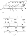
- a display device in accordance with the invention includes a cathode, illustrated in cross-section in Figure 1, comprising a conductive substrate 1 supporting conductive substantially conical field emission tips 2 typically between 1 and 2 microns in height and with bases about 1 micron across.
- This structure is overlain by an insulating layer 3, typically between 1 and 2 microns thick, itself overlain by a thin electrically conductive layer, typically 0.3 microns thick, which acts as a first grid 4 and has circular apertures 5 exposing the underlying tips placed concentric with those tips.
- the grid 4 is further covered by an additional insulator layer 6 and a second metal layer which acts as a second grid 7 and also has apertures 8 centred about the axis of the tips perpendicular to the substrate 1.
- the apertures in the second grid 7 are typically larger than those in the first and for a first grid aperture of 1.5 microns diameter the second grid typically has a 3 micron diameter. It should be noted that the particular dimensions are only given by way of example and that they could differ substantially depending on the fabrication methods employed and on the particular application requirements.
- Each of the grids 4 and 7 comprises parallel strips of conductive material, those of the first being arranged orthogonal to those of the second as shown in Figure 2 to provide matrix addressing of patches of tips at their crossing points.
- Each patch contains one or more tips aligned with grid apertures in one column of the first grid 4 and in one row of the second grid 7.
- a method for fabricating an array of tips is described in our co-pending patent application published under serial number GB 2254958A.
- the tips must be electrically conducting and may be composed of the same material as that of the substrate, typically silicon, they could be formed of a different material (molybdenum for example) possibly on an insulating substrate such as a silica glass. Whether the tips are of silicon, molybdenum or another material they may be connected to a common electrical supply (not shown) but may also consist of electrically isolated patches, for example on an insulating substrate, and be separately addressable.
- the cathode is operated by typically applying +60 V to the first grid 4 and + 4 V to the second grid 7 to provide an average emission current greater than 10 nA from each tip. Emission is switched off either by reducing the first grid voltage to about 35 V or by preventing emissions passing the second grid 7 with a second grid bias close to zero. Such a bias reflects the emission back to the first grid 4. Biasing the second grid 7 at about -20 V not only reflects the emission but also suppresses the magnitude of the current, typically to less than a tenth of its "on" value. Thus a modulation of 25 V in the biases on the two grids provides a means of turning on a particular patch within a large array of patches. Sequential addressing of the rows and columns of the grids 4 and 7 results in a time multiplexed emission pattern from the array of cathode patches.
- the performance of this cathode may be further enhanced by having the first grid 4 composed of a very resistive material such as polysilicon or amorphous silicon.
- emission is further suppressed by the charging of the first grid 4 when emission is switched back to it by negative bias on the second grid 7.
- This enables the complete emission to be switched off by as little as minus one volt applied to the second grid 7 as a consequence of the low energy spread of field emitted electrons.
- a resistive grid tends to suppress emission from the most emissive tips of the array thus providing a mechanism for reducing emissive current variation across the array of emitter patches.
- Such a resistive grid also provides a soft failure mechanism whereby the current resulting from an electrical short between the first and second grid or between the first grid and the tips will not lead to destructing high leakage current.
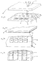
- the first grid 4 preferably includes a coarse mesh of conductive material 9 beneath or overlying the high resistivity grid film. Examples of two such structures are shown in Figures 3a and 3b.
- any emission current which depends on the voltage of the first grid, will form an approximately collimated beam emerging perpendicular from the cathode surface.
- a sufficiently high electric field typically several hundreds of volts per millimetre, in the region above the cathode surface, the resulting angular spread of the beam may have full angular spreads of about one degree or less.
- the optimal angular spread and the second grid voltage required depends on this external field and on the potential of the first grid.
- the actual second grid voltage required to switch off the emission is close to the tip voltage plus the work function of the second grid material but is suppressed by both high field above the cathode and by high first grid voltages.
- emission currents reflected back to the first grid by a sufficiently higher second grid bias may also be transmitted by slight increases of the first grid voltage.
- suitable cathode geometries to switch the emission from cathode patches by modulation of only a few volts on both first and second grids, provided the first grid is sufficiently resistive to suppress the emission current from the tips whenever it is reflected back to the first grid. In the absence of such a mechanism the cathode would tend to be subjected to excessive heating and reduced efficiency.
- the collimated nature of the emission from a cathode in accordance with the invention results in a number of devices incorporating such a cathode becoming viable.
- the anode consists of a phosphor coated conducting glass sheet
- the matrix addressed cathode is capable of producing light emission from regions of the glass anode 12 having diameters of less than one hundred microns by irradiation with electron emission from patches of the underlying cathodes switched on by application of suitable voltages to a row and column via contact pads 10, as shown in Figure 4.
- the relatively large gap between the cathode and glass anode permits a relatively high voltage, typically between + 1000 V and + 10,000 V, to be applied to the anode relative to the cathode and high brightness to be obtained, at about 50% total power efficiency, with only a few tens of nanoamps of current from each cathode patch.
- the anode typically consists of a glass substrate 13 with a coating of Indium Tin Oxide (ITO) 14 and a coating 15 (which may be continuous, as shown, or segmented) of a phosphor material overlaying the ITO layer ( Figure 5a).
- ITO Indium Tin Oxide
- Suitable phosphors are conventional CRT phosphors, with or without metal coating, or if lower voltage operation is required fluorescent polymer materials, and particularly those based on polyphenylene vinylene, or any other low voltage phosphor.
- this phosphor layer may consist of an array of three different phosphor "dots" 16A, 16B and 16C as shown in Figure 5b.
- each dot is aligned with a corresponding one the cathode patches.
- the ITO may be patterned into parallel tracks 17 with the three different phosphors 16A, 16B and 16C applied sequentially to each in turn as in Figure 5c so that the phosphor to be irradiated is selected by applying the anode bias sequentially to each anode ITO track in turn.
- the relatively large gap between the anode and cathode and the presence of electron beams within the intervening gap makes it difficult to support the anode by pillars within the areas of the cathode.
- Support may be achieved by using insulating spacers 18 around the periphery of the cathode, positioned between the cathode substrate and anode plate 13 as shown in Figure 6.
- the whole sandwich structure is then sealed into an external vacuum tight envelope (not shown) capable of maintaining a high vacuum, typically about 10 ⁇ 6 mbar.
- the envelope may be transparent to visible radiation or in other parts of the electromagnetic spectrum.
- the external envelope which may have curved walls, results in no structural support being required within the area of the cathode between it and the anode since in this implementation vacuum is maintained within and outside the cathode-anode gap.
- the drive electronics for the time multiplexed addressing of individual cathode patches are also accommodated within the external envelope so that only a small number of electrical connections need to be made through the wall of the vacuum envelope.
- the drive circuitry might also advantageously be fabricated on the substrate of the cathode structure where this is of silicon or some other appropriate material.
- the cathode is fabricated on a single substrate it might also be built up from a number of separate cathode tiles.
- the anode consists of a single glass sheet,in another embodiment of the invention, a number of separate cathode and anode modules could be included within the one envelope.
- the device With a phosphor coated anode the device provides a visible display. If the anode comprises an infra-red transparent material such as quartz or sapphire and the conducting layer is a thin metal sheet then the device can provide an infra-red display. In this case, higher electrical currents are required such that the combination of high current and high anode voltage gives significant anode heating.
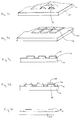
- the performance of such a device may be improved by having an anode structure which includes a thin metal sheet 21 in the form of multiple bridge structures 19, as shown in Figure 7a, in which there are unsupported regions of metal with a vacuum (or gas) gap between the metal and the anode substrate 20. Similar constructions are disclosed in our previous application published under serial number GB 2209432A.
- Such structures may be formed by firstly coating the IR transparent material 20 with a sacrificial material, such as a CVD deposited silica glass on an organic resist, patterning it to leave only pillars 22 of the material (as shown in Figure 7b); coating the whole surface with a thin metal layer 21 ( Figure 7c); patterning this layer with a resist mask 23 with apertures 24 over the edges of the metal domes ( Figure 7d) and etching away the exposed metal. The resist is then removed and the sacrificial layer dissolved via the apertures formed in the metal layer. Thus regions of thin metal are formed supported only by their edges (as shown in Figure 7e).
- a sacrificial material such as a CVD deposited silica glass on an organic resist
- these the bridge structures might advantageously be aligned directly above corresponding cathode patches on the cathode substrate and by sequentially addressing the rows and columns of the cathode array a dynamic (in this case infra-red) emission scene may be displayed on the anode surface.
Applications Claiming Priority (2)
| Application Number | Priority Date | Filing Date | Title |
|---|---|---|---|
| GB9326151A GB2285168B (en) | 1993-12-22 | 1993-12-22 | Electron field emission devices |
| GB9326151 | 1993-12-22 |
Publications (2)
| Publication Number | Publication Date |
|---|---|
| EP0660368A1 true EP0660368A1 (de) | 1995-06-28 |
| EP0660368B1 EP0660368B1 (de) | 1997-09-10 |
Family
ID=10747001
Family Applications (1)
| Application Number | Title | Priority Date | Filing Date |
|---|---|---|---|
| EP94309691A Expired - Lifetime EP0660368B1 (de) | 1993-12-22 | 1994-12-22 | Feldemissionselektronenvorrichtung |
Country Status (4)
| Country | Link |
|---|---|
| US (1) | US5942849A (de) |
| EP (1) | EP0660368B1 (de) |
| DE (1) | DE69405529T2 (de) |
| GB (1) | GB2285168B (de) |
Cited By (11)
| Publication number | Priority date | Publication date | Assignee | Title |
|---|---|---|---|---|
| EP0714111A1 (de) * | 1994-11-25 | 1996-05-29 | Motorola, Inc. | Kollimations-Extraktionsgitterleiter und Verfahren zur Fokussierung eines Elektronenstrahls |
| EP0734043A1 (de) * | 1995-03-22 | 1996-09-25 | Pixtech S.A. | Doppel-Gate-Flaches Bildschirm |
| FR2737041A1 (fr) * | 1995-07-07 | 1997-01-24 | Nec Corp | Canon a electrons pourvu d'une cathode froide a emission de champ |
| FR2748348A1 (fr) * | 1996-05-06 | 1997-11-07 | Pixtech Sa | Ecran couleur a micropointes a double grille |
| EP0854493A1 (de) * | 1997-01-16 | 1998-07-22 | International Business Machines Corporation | Kathode für eine Bildanzeigevorrichtung |
| EP1037250A1 (de) * | 1999-03-18 | 2000-09-20 | Matsushita Electric Industrial Co., Ltd. | Elektronenemittierendes Element und Bildausgabevorrichtung |
| EP1096542A1 (de) * | 1999-10-28 | 2001-05-02 | Pixtech S.A. | Flasches Bildschirm mit Schutzgitter |
| WO2001031672A1 (fr) * | 1999-10-28 | 2001-05-03 | Commissariat A L'energie Atomique | Procede de commande de structure comportant une source d'electrons a effet de champ |
| FR2800511A1 (fr) * | 1999-10-28 | 2001-05-04 | Pixtech Sa | Ecran plat de visualisation a grille de protection |
| US6692327B1 (en) | 1999-01-13 | 2004-02-17 | Matsushita Electric Industrial Co., Ltd. | Method for producing electron emitting element |
| EP1511059A1 (de) * | 2003-08-27 | 2005-03-02 | Electronics And Telecommunications Research Institute | Feldemissionsanordnung |
Families Citing this family (9)
| Publication number | Priority date | Publication date | Assignee | Title |
|---|---|---|---|---|
| US6559818B1 (en) * | 1995-01-24 | 2003-05-06 | Micron Technology, Inc. | Method of testing addressable emissive cathodes |
| US5751262A (en) | 1995-01-24 | 1998-05-12 | Micron Display Technology, Inc. | Method and apparatus for testing emissive cathodes |
| DE19534228A1 (de) * | 1995-09-15 | 1997-03-20 | Licentia Gmbh | Kathodenstrahlröhre mit einer Feldemissionskathode |
| US6137213A (en) * | 1998-10-21 | 2000-10-24 | Motorola, Inc. | Field emission device having a vacuum bridge focusing structure and method |
| JP3397738B2 (ja) | 1999-02-25 | 2003-04-21 | キヤノン株式会社 | 電子源および画像形成装置 |
| US6225687B1 (en) * | 1999-09-02 | 2001-05-01 | Intel Corporation | Chip package with degassing holes |
| US6429596B1 (en) * | 1999-12-31 | 2002-08-06 | Extreme Devices, Inc. | Segmented gate drive for dynamic beam shape correction in field emission cathodes |
| KR20040034251A (ko) * | 2002-10-21 | 2004-04-28 | 삼성에스디아이 주식회사 | 전계방출소자 |
| CN100395863C (zh) * | 2004-04-30 | 2008-06-18 | 东元奈米应材股份有限公司 | 四极场发射显示器 |
Citations (8)
| Publication number | Priority date | Publication date | Assignee | Title |
|---|---|---|---|---|
| EP0349425A1 (de) * | 1988-06-29 | 1990-01-03 | Commissariat A L'energie Atomique | Dreifarben-Leuchtschirm mit Mikrospitzen-Kathoden |
| EP0391139A2 (de) * | 1989-04-07 | 1990-10-10 | Nokia (Deutschland) GmbH | Flache Anzeigeeinrichtung |
| EP0404022A2 (de) * | 1989-06-19 | 1990-12-27 | Matsushita Electric Industrial Co., Ltd. | Flache Bildwiedergabevorrichtung und Verfahren zur Herstellung derselben |
| EP0494425A2 (de) * | 1990-12-28 | 1992-07-15 | Sony Corporation | Flache Anzeigeeinrichtung und Herstellungsverfahren derselben |
| EP0497509A1 (de) * | 1991-01-25 | 1992-08-05 | Gec-Marconi Limited | Verfahren zur Herstellung einer Feldemissionvorrichtung |
| EP0501785A2 (de) * | 1991-03-01 | 1992-09-02 | Raytheon Company | Elektronenemittierende Struktur und Herstellungsverfahren |
| EP0545621A1 (de) * | 1991-11-29 | 1993-06-09 | Motorola, Inc. | Herstellungsverfahren einer Feldemissionsvorrichtung mit integraler elektrostatischer Linsenanordnung |
| US5235244A (en) * | 1990-01-29 | 1993-08-10 | Innovative Display Development Partners | Automatically collimating electron beam producing arrangement |
Family Cites Families (7)
| Publication number | Priority date | Publication date | Assignee | Title |
|---|---|---|---|---|
| JPS5235491B2 (de) * | 1972-02-16 | 1977-09-09 | ||
| US3935500A (en) * | 1974-12-09 | 1976-01-27 | Texas Instruments Incorporated | Flat CRT system |
| DE3235724A1 (de) * | 1981-10-02 | 1983-04-21 | Futaba Denshi Kogyo K.K., Mobara, Chiba | Leuchtstoff-anzeigevorrichtung |
| FR2568394B1 (fr) * | 1984-07-27 | 1988-02-12 | Commissariat Energie Atomique | Dispositif de visualisation par cathodoluminescence excitee par emission de champ |
| EP0316871B1 (de) * | 1987-11-16 | 1994-11-30 | Matsushita Electric Industrial Co., Ltd. | Bildwiedergabevorrichtung |
| US5424605A (en) * | 1992-04-10 | 1995-06-13 | Silicon Video Corporation | Self supporting flat video display |
| US5336888A (en) * | 1992-07-30 | 1994-08-09 | Aerojet-General Corporation | High resolution infrared scene simulator |
-
1993
- 1993-12-22 GB GB9326151A patent/GB2285168B/en not_active Expired - Fee Related
-
1994
- 1994-12-22 EP EP94309691A patent/EP0660368B1/de not_active Expired - Lifetime
- 1994-12-22 DE DE69405529T patent/DE69405529T2/de not_active Expired - Fee Related
-
1997
- 1997-05-21 US US08/861,186 patent/US5942849A/en not_active Expired - Fee Related
Patent Citations (8)
| Publication number | Priority date | Publication date | Assignee | Title |
|---|---|---|---|---|
| EP0349425A1 (de) * | 1988-06-29 | 1990-01-03 | Commissariat A L'energie Atomique | Dreifarben-Leuchtschirm mit Mikrospitzen-Kathoden |
| EP0391139A2 (de) * | 1989-04-07 | 1990-10-10 | Nokia (Deutschland) GmbH | Flache Anzeigeeinrichtung |
| EP0404022A2 (de) * | 1989-06-19 | 1990-12-27 | Matsushita Electric Industrial Co., Ltd. | Flache Bildwiedergabevorrichtung und Verfahren zur Herstellung derselben |
| US5235244A (en) * | 1990-01-29 | 1993-08-10 | Innovative Display Development Partners | Automatically collimating electron beam producing arrangement |
| EP0494425A2 (de) * | 1990-12-28 | 1992-07-15 | Sony Corporation | Flache Anzeigeeinrichtung und Herstellungsverfahren derselben |
| EP0497509A1 (de) * | 1991-01-25 | 1992-08-05 | Gec-Marconi Limited | Verfahren zur Herstellung einer Feldemissionvorrichtung |
| EP0501785A2 (de) * | 1991-03-01 | 1992-09-02 | Raytheon Company | Elektronenemittierende Struktur und Herstellungsverfahren |
| EP0545621A1 (de) * | 1991-11-29 | 1993-06-09 | Motorola, Inc. | Herstellungsverfahren einer Feldemissionsvorrichtung mit integraler elektrostatischer Linsenanordnung |
Cited By (21)
| Publication number | Priority date | Publication date | Assignee | Title |
|---|---|---|---|---|
| EP0714111A1 (de) * | 1994-11-25 | 1996-05-29 | Motorola, Inc. | Kollimations-Extraktionsgitterleiter und Verfahren zur Fokussierung eines Elektronenstrahls |
| EP0734043A1 (de) * | 1995-03-22 | 1996-09-25 | Pixtech S.A. | Doppel-Gate-Flaches Bildschirm |
| FR2732159A1 (fr) * | 1995-03-22 | 1996-09-27 | Pixtech Sa | Ecran plat de visualisation a double grille |
| US5764204A (en) * | 1995-03-22 | 1998-06-09 | Pixtech S.A. | Two-gate flat display screen |
| FR2737041A1 (fr) * | 1995-07-07 | 1997-01-24 | Nec Corp | Canon a electrons pourvu d'une cathode froide a emission de champ |
| FR2748348A1 (fr) * | 1996-05-06 | 1997-11-07 | Pixtech Sa | Ecran couleur a micropointes a double grille |
| EP0806790A1 (de) * | 1996-05-06 | 1997-11-12 | Pixtech S.A. | Mikrospitzen-Farbbildschirm mit zwei Gittern |
| US6034658A (en) * | 1996-05-06 | 2000-03-07 | Pixtech Sa | Double grid microtip color screen |
| EP0854493A1 (de) * | 1997-01-16 | 1998-07-22 | International Business Machines Corporation | Kathode für eine Bildanzeigevorrichtung |
| US5889372A (en) * | 1997-01-16 | 1999-03-30 | International Business Machines Corporation | Device cathode with extractor grid for display |
| US6692327B1 (en) | 1999-01-13 | 2004-02-17 | Matsushita Electric Industrial Co., Ltd. | Method for producing electron emitting element |
| EP1037250A1 (de) * | 1999-03-18 | 2000-09-20 | Matsushita Electric Industrial Co., Ltd. | Elektronenemittierendes Element und Bildausgabevorrichtung |
| US6400091B1 (en) | 1999-03-18 | 2002-06-04 | Matsushita Electric Industrial Co., Ltd. | Electron emission element and image output device |
| WO2001031672A1 (fr) * | 1999-10-28 | 2001-05-03 | Commissariat A L'energie Atomique | Procede de commande de structure comportant une source d'electrons a effet de champ |
| FR2800512A1 (fr) * | 1999-10-28 | 2001-05-04 | Pixtech Sa | Ecran plat de visualisation a grille de protection |
| FR2800511A1 (fr) * | 1999-10-28 | 2001-05-04 | Pixtech Sa | Ecran plat de visualisation a grille de protection |
| FR2800510A1 (fr) * | 1999-10-28 | 2001-05-04 | Commissariat Energie Atomique | Procede de commande de structure comportant une source d'electrons a effet de champ |
| US6462486B1 (en) | 1999-10-28 | 2002-10-08 | Commissariat A L'energie Atomique | Method for controlling a structure comprising a source of field emitting electrons |
| US6683415B1 (en) | 1999-10-28 | 2004-01-27 | Pixtech, S.A. | Flat display screen with a protection grid |
| EP1096542A1 (de) * | 1999-10-28 | 2001-05-02 | Pixtech S.A. | Flasches Bildschirm mit Schutzgitter |
| EP1511059A1 (de) * | 2003-08-27 | 2005-03-02 | Electronics And Telecommunications Research Institute | Feldemissionsanordnung |
Also Published As
| Publication number | Publication date |
|---|---|
| DE69405529D1 (de) | 1997-10-16 |
| US5942849A (en) | 1999-08-24 |
| GB2285168A (en) | 1995-06-28 |
| EP0660368B1 (de) | 1997-09-10 |
| DE69405529T2 (de) | 1998-01-15 |
| GB9326151D0 (en) | 1994-02-23 |
| GB2285168B (en) | 1997-07-16 |
Similar Documents
| Publication | Publication Date | Title |
|---|---|---|
| EP0660368B1 (de) | Feldemissionselektronenvorrichtung | |
| JP2809129B2 (ja) | 電界放射冷陰極とこれを用いた表示装置 | |
| EP0025221B1 (de) | Flache Anzeigevorrichtung | |
| KR100312694B1 (ko) | 카본 나노튜브 필름을 전자 방출원으로 사용하는 전계 방출 표시 장치 | |
| US5477105A (en) | Structure of light-emitting device with raised black matrix for use in optical devices such as flat-panel cathode-ray tubes | |
| EP1511059B1 (de) | Feldemissionsanordnung | |
| US5578900A (en) | Built in ion pump for field emission display | |
| WO1995020821A1 (en) | Field emitter with focusing ridges | |
| KR100597056B1 (ko) | 대면적 fed 장치 및 그 제조 방법 | |
| US6028391A (en) | Field emission device having spherically curved electron emission layer and spherically recessed substrate | |
| KR20010031360A (ko) | 전계 방출 디바이스 | |
| US5955833A (en) | Field emission display devices | |
| US5920151A (en) | Structure and fabrication of electron-emitting device having focus coating contacted through underlying access conductor | |
| GB2313703A (en) | Current sensing in vacuum electron devices | |
| US6008577A (en) | Flat panel display with magnetic focusing layer | |
| US20050264165A1 (en) | Electron emission device including enhanced beam focusing and method of fabrication | |
| US7704117B2 (en) | Electron emission display and method of fabricating mesh electrode structure for the same | |
| US6013974A (en) | Electron-emitting device having focus coating that extends partway into focus openings | |
| US20050140268A1 (en) | Electron emission device | |
| US6215242B1 (en) | Field emission display device having a photon-generated electron emitter | |
| US5886461A (en) | Transparent conductor for field emission displays | |
| EP1159752B1 (de) | Kathodenstruktur für eine feldemissionsanzeigevorrichtung | |
| CN102254765A (zh) | 场发射装置的制备方法 | |
| RU2115194C1 (ru) | Электронно-оптическая система, матричная электронно-оптическая система, устройства на их основе (варианты) | |
| US20030178945A1 (en) | Reflective edge field-emission pixel and associated display |
Legal Events
| Date | Code | Title | Description |
|---|---|---|---|
| PUAI | Public reference made under article 153(3) epc to a published international application that has entered the european phase |
Free format text: ORIGINAL CODE: 0009012 |
|
| AK | Designated contracting states |
Kind code of ref document: A1 Designated state(s): DE FR |
|
| 17P | Request for examination filed |
Effective date: 19951218 |
|
| 17Q | First examination report despatched |
Effective date: 19960201 |
|
| GRAG | Despatch of communication of intention to grant |
Free format text: ORIGINAL CODE: EPIDOS AGRA |
|
| GRAH | Despatch of communication of intention to grant a patent |
Free format text: ORIGINAL CODE: EPIDOS IGRA |
|
| GRAH | Despatch of communication of intention to grant a patent |
Free format text: ORIGINAL CODE: EPIDOS IGRA |
|
| GRAA | (expected) grant |
Free format text: ORIGINAL CODE: 0009210 |
|
| AK | Designated contracting states |
Kind code of ref document: B1 Designated state(s): DE FR |
|
| REF | Corresponds to: |
Ref document number: 69405529 Country of ref document: DE Date of ref document: 19971016 |
|
| ET | Fr: translation filed | ||
| PLBE | No opposition filed within time limit |
Free format text: ORIGINAL CODE: 0009261 |
|
| STAA | Information on the status of an ep patent application or granted ep patent |
Free format text: STATUS: NO OPPOSITION FILED WITHIN TIME LIMIT |
|
| 26N | No opposition filed | ||
| PGFP | Annual fee paid to national office [announced via postgrant information from national office to epo] |
Ref country code: FR Payment date: 20031210 Year of fee payment: 10 |
|
| PGFP | Annual fee paid to national office [announced via postgrant information from national office to epo] |
Ref country code: DE Payment date: 20040102 Year of fee payment: 10 |
|
| PG25 | Lapsed in a contracting state [announced via postgrant information from national office to epo] |
Ref country code: DE Free format text: LAPSE BECAUSE OF NON-PAYMENT OF DUE FEES Effective date: 20050701 |
|
| PG25 | Lapsed in a contracting state [announced via postgrant information from national office to epo] |
Ref country code: FR Free format text: LAPSE BECAUSE OF NON-PAYMENT OF DUE FEES Effective date: 20050831 |
|
| REG | Reference to a national code |
Ref country code: FR Ref legal event code: ST |