EP0651501B1 - Power amplifier having multiple switched stages - Google Patents
Power amplifier having multiple switched stages Download PDFInfo
- Publication number
- EP0651501B1 EP0651501B1 EP95100838A EP95100838A EP0651501B1 EP 0651501 B1 EP0651501 B1 EP 0651501B1 EP 95100838 A EP95100838 A EP 95100838A EP 95100838 A EP95100838 A EP 95100838A EP 0651501 B1 EP0651501 B1 EP 0651501B1
- Authority
- EP
- European Patent Office
- Prior art keywords
- stages
- state
- source
- amplifier
- response
- Prior art date
- Legal status (The legal status is an assumption and is not a legal conclusion. Google has not performed a legal analysis and makes no representation as to the accuracy of the status listed.)
- Revoked
Links
Images
Classifications
-
- H—ELECTRICITY
- H03—ELECTRONIC CIRCUITRY
- H03F—AMPLIFIERS
- H03F3/00—Amplifiers with only discharge tubes or only semiconductor devices as amplifying elements
- H03F3/20—Power amplifiers, e.g. Class B amplifiers, Class C amplifiers
- H03F3/21—Power amplifiers, e.g. Class B amplifiers, Class C amplifiers with semiconductor devices only
- H03F3/217—Class D power amplifiers; Switching amplifiers
- H03F3/2178—Class D power amplifiers; Switching amplifiers using more than one switch or switching amplifier in parallel or in series
-
- H—ELECTRICITY
- H03—ELECTRONIC CIRCUITRY
- H03F—AMPLIFIERS
- H03F3/00—Amplifiers with only discharge tubes or only semiconductor devices as amplifying elements
- H03F3/20—Power amplifiers, e.g. Class B amplifiers, Class C amplifiers
- H03F3/24—Power amplifiers, e.g. Class B amplifiers, Class C amplifiers of transmitter output stages
Definitions
- the present invention relates generally to power amplifiers particularly adapted to provide modulation for an output stage of an AM RF amplifier. More particularly, the invention relates to a power amplifier including multiple stages for selectively coupling power from a DC power supply to a load, wherein responses from the multiple stages are summed together and the number of stages that couple power to the load is determined by the amplitude of a signal source.
- Power amplifiers of the pulse width modulated type are frequently used to provide modulating inputs to an output electrode of an output stage of a high power AM, RF transmitter.
- Some of the prior art technologies for supplying a modulating input to an output stage of a high power AM RF amplifier are Class B push-pull amplifiers and Class D pulse width modulation amplifiers.
- Exemplary of prior art patents disclosing such modulation sources are Hulsey et al., United States Patents 4,747,161 and 4,776,036, Weaver, 4,896,372, as well as Cummings 4,140,980, Swanson 3,506,920 and Swanson 3,588,744.
- the modulating waveform controls the voltage supplied to the anode, i.e., plate, or output electrode, of a power transmitting tube.
- the plate DC power supply voltage of the output tube is varied in response to an analog modulation source.
- pulse width modulated, Class D amplifiers produce varying output signals by changing the on and off times, i.e., duty cycle and frequency, of a switch connected between a DC power supply and the plate of the output stage.
- the amplitude, as well as duration, of current and voltage fed by the switched supply to the output stage is varied.
- the variable duration current pulses are coupled to the anode of the output stage via a low pass filter, to substantially reconstruct the original analog input signal to the power amplifier.
- some power amplifiers use multiple pulse width modulation stages controlled by phase displaced pulses having the same duty cycle; see, e.g., U.S. Patents Swanson 4,468,626, Swanson 4,164,714 and Kyrian et al 4,369,409.
- these modulators referred to in the art as polyphase pulse width modulators, the stages are switched at the same frequency, but with relative phase differences. The power fed through the multiple stages is summed.
- a disadvantage of the polyphase pulse width modulation arrangement is that usually all of the stages are being switched simultaneously. This results in all of the stages being susceptible to narrow pulse distortion, as described in Hulsey, U.S. Patent 4,776,036.
- a problem with the polyphase pulse width modulation source is that the modulating output voltage is in certain instances not an accurate replica of the analog signal supplied to the device. This results in distortion of the modulating waveform, with resulting distortion in the transmitted signal of the AM RF transmitter.
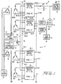
- the transmitter includes high power output stage 11 including tetrode tube 12, antenna coupling network 13, screen supply 14, DC bias source 15 and r.f. carrier source 16.
- Bias source 15 and carrier source 16 are selected so that tetrode 12 is activated to be driven in any of Class B, C, or G.
- a modulation voltage is applied as the power supply voltage for the anode, i.e., plate, of tetrode 12 by a modulation source including modulator 17.
- modulator 17 is a high power amplifier responsive to AC analog modulation source 18, typically an audio, voice source that varies between a zero voltage level and a predetermined maximum level.
- Tetrode 12 responds to the outputs of sources 15 and 16, the voltage of supply 14 and the variable amplitude DC voltage applied to plate 11 thereof to derive an amplitude modulated wave having a center frequency equal to that of carrier source 16.
- the wave derived by tetrode 12 is applied to antenna 19 by way of antenna coupling network 13.
- Power amplifier 17 derives a variable amplitude, variable frequency wave that is approximately a replica of the wave derived by source 18.
- the wave derived by amplifier 17, however, has step variations at discrete voltage levels. Typically, the step variations are approximately 600 volts. In one embodiment, 48 different steps subsist between the minimum and maximum voltages derived by amplifier 17 so the maximum voltage is approximately 28,800 volts, at a power level of about 500 kilowatts.
- the output of amplifier 17 is smoothed or averaged by low pass filter 21 as it is applied to the plate of tetrode 12 so that the tetrode plate voltage is a close replica of the wave of source 18.
- power amplifier 17 includes 48 different stages 34.1, 34.2, 34.3...34.46, 34.47 and 34.48; for convenience only the first two and last two stages, i.e., stages 34.1, 34.2, 34.47 and 34.48, are illustrated.
- stages 34.1, 34.2, 34.47 and 34.48 Like components of the different identical stages bear the same reference numerals to the left of a decimal point, while components of the same stage have the same reference numeral, equal to the stage number, to the right of the decimal point.
- stage 34.1 is discussed in detail. Since all of stages 34 are the same, the discussion of stage 34.1 is generally sufficient for all of the stages.
- the number of stages can be greater or smaller than 48, but in any event at least several stages are provided.
- Responses from all of stages 34 are summed together by adding output voltages of the different stages together.
- the output voltages are added together by stacking the voltages at the output terminals of the different stages together.
- Each of stages 34 is selectively in a fully sourced, i.e., saturated, state or a non-sourced state.
- Each of stages 34 is powered by a DC source having the same voltage. While each stage is in a fully conducting (saturated) state, the DC voltage applied to the particular stage is applied to output terminals 41 and 42 of the stage. While a particular stage 34 is non-sourced, the output voltage and output impedance of the stage drop virtually to zero.
- Output terminals 41 and 42 are connected in series between ground and the input of low pass filter 21. Hence, terminal 41.1 is grounded, terminals 42.1 and 41.2 are connected together as are terminals 42.47 and 41.48, while terminal 42.48 is connected to filter 21. The sum of the voltages at output terminals 41 and 42, as derived at terminal 42.48, is thus supplied as a variable amplitude DC voltage to low pass filter 21.
- DC power for each of stages 34 is derived from three-phase AC power source 51.
- Source 51 drives delta connected primary windings 52 and 53 of transformers 54 and 55 in parallel.
- Winding 52 drives isolated wye connected three-phase secondary windings 56.1-56.24 while transformer 53 drives similarly connected secondary windings 56.25-56.48.
- Primary windings 52 and 53 include taps (not shown), adjusted so that the AC current flowing into each of stages 34 is approximately in phase with the voltage developed across the AC input terminals of the particular stage; in other words, the power factor of the power supplied to each of stages 34 is close to unity while the particular stage is conducting, to maximize efficiency.
- Each of stages 34 includes a full wave three-phase rectifier (not shown) for converting the three-phase input of the particular stage into a DC voltage having relatively low ripple and constant amplitude.
- Each of stages 34 is driven in parallel by the output of AC analog modulation source 18.
- Each of stages 34 has a different threshold for the output voltage level of source 18. The different thresholds are established by connecting resistive voltage divider 61 between a positive DC voltage at terminal 62 and ground. Voltage divider 61 includes a different tap 65 for each of stages 34. Equal valued resistors 63 are connected between adjacent taps so the voltage difference between adjacent taps is the same. In one embodiment, the voltage of source 62 is 4.8 volts so the voltages at taps 65.1, 65.2...65.47 and 65.48 are respectively 0, 0.1...4.7 and 4.8 volts.
- the threshold values applied by taps 65 of voltage divider 61 to stages 34 are compared with an analog voltage on lead 64. In response to the threshold of a particular stage 34 being less than the voltage applied to that stage by the voltage on lead 64 the particular stage is activated into a fully conducting, saturated state. In response to the threshold applied by voltage divider 61 to a particular stage being greater than the voltage applied to the stage via lead 64, the particular stage is in a non-sourced state.
- Stage 34.1 is connected to a grounded tap of voltage divider 61 so that stage 34.1 is conducting whenever the voltage on lead 64 exceeds a zero amplitude, which is the vast majority of the time.
- Stage 34.48 is activated into a fully conducting, saturated state for only a small percentage of the operating time of the amplifier. In the discussed embodiment, stage 34.1 is conducting at all times except a portion of the time while the voltage of source 18 is less than 0.05 volts; stage 34.48 is fully conducting only a portion of the time the voltage of source 18 exceeds 4.75 volts.
- each of stages 34.1 and 34.48 has a 50% duty cycle, respectively.
- the voltage of source 18 varies between slightly more than 0.05 volts to slightly less than 4.75 volts intermediate ones of stages 34, i.e., stages 34.2-34.47, are in fully conducting and non-sourced states for variable times that primarily are a function of the amplitude of source 18.
- the number of fully conducting stages is basically a linear function of the amplitude of source 18.
- Each of stages 34 is activated between a fully conducting and non-sourced state as a function of the amplitude of audio source 18, the threshold voltage applied to the particular stage by voltage divider 61 and a factor that effectively varies the threshold of all of the stages simultaneously multiple times during each cycle of source 18.
- the variation in effective threshold level of each stage 34 is by an amount at least equal to the threshold between adjacent stages.
- the threshold variation was equal to the difference between adjacent thresholds. It was found that such variations materially reduced the distortion of the modulating voltage applied by low pass filter 21 to the plate of tetrode 12 relative to the situation that would have occurred without a variable threshold. It is also feasible for the threshold variation to be equal to the threshold of more than one stage, as long as the threshold variation is only a small percentage of the maximum voltage of source 18. If the threshold variation is twice the threshold between an adjacent pair of stages 34, the outputs of the two stages are averaged and eliminate control problems for the voltages at taps 65.
- the variable threshold for stages 34 is attained by linearly combining the output of triangular wave source 71 with the output of source 18 in summing network 72.
- Triangular wave source 71 has a minimum frequency that is at least twice and preferably several times the highest frequency of source 18.
- the maximum voltage amplitude of the output of triangle wave source 71 is constant at a relatively small percentage of the maximum amplitude derived by source 18. Since source 71 effectively varies the threshold of each of stages 34, the maximum voltage amplitude of the wave derived by source 71 is at least equal to the difference between the threshold of adjacent pairs of stages 34.
- Source 71 is preferably a triangular or linear sawtooth wave, to provide maximum linearity and minimize distortion in the signal coupled by low pass filter 21 to the plate of tetrode 12. Linearity is achieved because the conducting time of each output stage 34 that is switched is directly proportional to the instantaneous amplitude of the voltage of source 18; hence the switched stage 34 is pulse width modulated. While source 71 preferably has a linear variation other waveforms could be used for this source. For example, source 71 could, in certain situations, be a sine wave.
- Enhanced linearity is achieved by varying the frequency of source 71 as a function of the amplitude and frequency of the output of source 18. As the frequency and amplitude of source 18 increase, the frequency of source 71 increases accordingly. To this end, the output of source 18 is coupled to an input of source 71. It is to be understood, however, that source 71 can also be a constant frequency source that is unresponsive to the output of source 18.
- source 71 is constructed in a manner illustrated in Fig. 6 of previously mentioned United States Patent 4,896,372.
- the variable frequency, constant amplitude triangular wave derived from source 71 has a frequency that increases and decreases as an RMS-like function of the amplitude of source 18.
- the frequency of the triangular wave output of source 71 increases and decreases as the frequency of source 18 increases and decreases.
- triangular wave source 71 is constructed identically to the triangular wave source and the components connected to the input thereof as disclosed in Fig. 6 of the aforementioned 4,896,372 patent.
- the duration of the time while a particular stage 34 is in a conducting state is primarily linearly related to the instantaneous amplitude of source 18, and is secondarily related to the RMS amplitude and frequency of source 18, for the reasons described supra in conjunction with the control of source 71.
- the output voltage of a particular stage 34 varies between zero and 600 volts in response to variations of source 18 while the voltage of source 18 varies between a median threshold for a particular stage and the peak-to-peak amplitude of triangular wave source 71.
- the duration of the 600 volt levels derived by a particular stage 34 is linearly related to the amplitude of source 18, as long as the amplitude of source 18 is between the median threshold for the stage, plus or minus the peak to peak amplitude of source 71.
- a particular stage 34 derives a pulse width modulated voltage that varies between zero and 600 volts.
- the average value of the pulses is proportional to variations of source 18 relative to the median threshold value of the particular stage.
- the pulse width modulated wave derived by stage 34.k is superimposed on the sum of the 600 volt outputs of stages 34.1 - 34.(k-1) so that the output of averaging filter 21 is a high voltage replica of the variations of source 18.
- stages 34 activated into a fully conducting state.
- summing circuit 72 deriving an instantaneous output level that is one-half of the voltage at terminal 62, half of the stages of amplifier 17 (viz: stages 34.1-35.24) are in a conducting state, while the remaining stages (viz: stages 34.25-34.48) are in a non-sourced state.
- the voltage at terminal 42.48 is a high voltage stair step waveform having 48 possible steps. While the voltage is at any one of the steps, variable width pulses having an amplitude of one step are derived. The widths of the pulses are linearly related to the instantaneous amplitude of source 18 in the threshold region for a particular one of stages 34. Because of the effective threshold variation provided by triangular wave source 71 for each of stages 34, the average value of the stair step wave at terminal 42.48 accurately tracks amplitude variations of source 18. Low pass, averaging filter 21 thereby derives an accurate high voltage replica of the waveform of source 18, without the switching losses associated with switching a high voltage source.
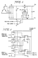
- FIG. 2 A circuit diagram for a preferred embodiment of each of stages 34 is illustrated in Fig. 2.
- Each of stages 34 is provided with DC power by three-phase rectifier 101 converting the three-phase AC voltage at secondary winding 56 of transformer 54 or 55 into a DC voltage.
- Rectifier 101 drives shunt capacitor 102 across which is developed a 600 volt DC power supply voltage.
- the voltage across capacitor 102 is selectively switched to output terminals 41 and 42 through the emitter collector path of isolated gate bipolar transistor 103 although other similar devices can be used.
- Transistor 103 has bipolar emitter-collector characteristics and high impedance gate, i.e., control electrode, characteristics similar to those of a metal oxide semiconductor field effect transistor.
- Transistor 103 includes collector and emitter electrodes respectively connected to one electrode of capacitor 102 and the cathode of diode 104.
- the anode of diode 104 is connected to the remaining electrode of capacitor 102.
- Diode 104 is connected across output terminals 41 and 42.
- Circuit 105 switches the emitter collector path of transistor 103 between a saturated and non-conducting state. In the saturated state, the DC voltage across capacitor 102 is coupled to terminals 41 and 42, while causing diode 104 to be back biased. When transistor 103 is not conducting, the voltage between terminals 41 and 42 drops quickly to zero by virtue of the relatively low impedance path provided through the anode and cathode of diode 104. Thereby, the impedance between terminals 41 and 42 is maintained at a first predetermined constant value while transistor 103 is in a conducting state, and is maintained at a second, much lower predetermined value while the transistor is not conducting.
- Circuit 105 is controlled by an opto-electronic link including photodiode 106, connected to input terminals of circuit 105 via current limiting resistor 107.
- Diode 106 is optically coupled (e.g. by a fiber optic link) to light emitting diode 108, connected via resistor 111 to be responsive to the output of comparator 109.
- Comparator 109 includes positive and negative input terminals 112 and 113, respectively responsive to the voltage at tap 65 of bias network 61 for the particular stage 34 and the voltage from summing network 72. In response to the signal at terminal 112 exceeding the voltage at terminal 113, comparator 109 derives a binary one output level. Comparator 109 derives a binary zero output level in response to the voltage at terminal 112, from bias network 61, being less than the voltage at terminal 113, from summing network 72.
- diode 108 In response to comparator 109 deriving a binary zero level, diode 108 is activated to illuminate photodiode 106. In contrast, diode 108 derives no optical signal in response to a binary one output of amplifier 109. In response to diode 106 being illuminated, circuit 105 is activated to cause transistor 103 to be in the saturated state. When no optical energy is incident on diode 106, transistor 103 does not conduct. The voltages from summing network 72 and bias network 61 are linearly combined to control the conducting state of the switch of stage 32 comprising transistor 103.
- a given analog input voltage causes different stages 34 to be activated to derive the same output voltage sum as is provided in the embodiment of Fig. 1 for the given voltage.
- Selection of which of stages 34 are conducting is a function of prior variations of AC modulation source 18, as well as the instantaneous value thereof. Insofar as the variations of modulation source 18 are random, the selection of which stages 34 is conducting is random. By randomizing which of stages 34 are conducting, certain stages are not almost always dissipating power, while other stages are virtually never dissipating power.
- each of stages 34 is pulse duration modulated at the frequency of triangular wave source 71.
- the number of stages 34 in a sourced state at a particular time is determined by the amplitude of signal source 18.
- the length of time each of stages 34 is sourced is also determined by the amplitude of signal source 18.
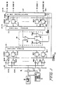
- the voltages of sources 18 and 71 are linearly combined in summing network 72 and compared in comparators 109.1-109.48 with the voltages at taps 65 on voltage divider 61.
- Comparators 109.1-109.48 derive binary levels in the same manner that binary levels are derived by the corresponding comparators 109 in stages 34.1-34.48 of Fig. 1.
- stages 34.7-34.30 may be conducting; during a subsequent instant stages 34.8-34.31 may be conducting.
- the number of comparators 109.1-109.48 deriving binary one levels is indicated by supplying the binary one output levels of these comparators to analog adding network 121.
- the output voltage of analog adding network 121 is a DC voltage having, at any one time, one of 48 possible values.
- Each of the possible output values of analog adder 121 represents the number of comparators 109.1-109.48 which is deriving a binary one level.
- comparators 109.1-109.48 are sampled many times during each cycle of triangle wave source 71 by respectively supplying the outputs of comparators 109.1-109.48 to sample and hold, i.e., latch, networks 122.1-122.48, also responsive to clock source 123, having a frequency of several megaHertz.
- the latched outputs of latches 122.1-122.48 are applied to analog summing circuit 121. As variations in modulation source 18 and wave source 71 occur, the output level of circuit 121 changes accordingly.
- the output signal of adder 121 is compared with a signal indicative of the number of stages 34 in a fully conducting state, as derived from analog adder 125.
- Adder 125 is responsive to latch networks 133.1-133.48 respectively responsive to 48 different binary states of ring modulator 127 and clock 123.
- Analog adder 125 derives an output having one of 48 different levels, each representing the conducting and non-conducting states of stages 34.1-34.48.
- the output signals of adders 121 and 125 are supplied to analog comparator 126 which selectively derives one of two positive going, i.e., binary zero to one, transitions as a function of the output signals of adders 121 and 125.
- Comparator 126 includes difference amplifier 140 as well as comparators 141 and 142; amplifier 140 has plus and minus inputs respectively responsive to the voltages derived by adders 121 and 125.
- the output of amplifier 140 is applied in parallel to negative and positive inputs of 141 and 142, having positive and negative inputs respectively responsive to negative and positive DC reference voltages, -Vref and +Vref, where Vref is typically 50 millivolts.
- comparator 141 derives a binary one level; in response to the voltage at the positive input of amplifier 142 exceeding +Vref, comparator 142 derives a binary one output. If the output of difference amplifier 140 is between a dead band from -Vref to +Vref, the outputs of comparators 141 or 142 are at the binary zero level and no changes occur in ring modulator 127.
- the transitions at the outputs of comparator 126 control which of output stages 34.1-34.48 are in conducting and non-sourced states.
- the outputs of comparator 126 are supplied to two separate input terminals of ring modulator 127, also responsive to clock source 123.
- Ring modulator 127 includes 48 output leads, one for each of output stages 34.1-34.48.
- the number of output stages 34 in a conducting state is generally equal to the number of comparators 109.1-109.48 deriving binary one levels. However, there is no other correlation between which of stages 34 are conducting and which of comparators 109.1-109.48 are deriving binary one levels.
- Ring modulator 127 includes two sets of output leads 128.1-128.48 and 129.1-129.48, respectively driven in parallel by binary signals representing which of stages 34.1-34.48 are fully conducting and non-sourced.
- the signals on output leads 128.1-128.48 are supplied as control inputs to stages 34.1-34.48.
- These controls include fiber optic links, as described supra with regard to Figs. 1 and 2.
- the signals on output leads 128.1-128.48 are supplied as inputs to latches 133.1-133.48, thence to analog adder 125.
- ring modulator 127 Details of a preferred embodiment of ring modulator 127 are illustrated in Fig. 4 as including two 48 stage recirculating shift registers 131 and 132 and 48 output latches 133.1-133.48, each configured as a J-K flip-flop.
- Each of shift registers 131 and 132 includes an increment (INC) input terminal responsive to a separate output of comparator network 126 and a clock input terminal responsive to clock source 123.
- Shift registers 131 and 132 are driven only in a forward direction, so that in response to transitions supplied to the increment inputs thereof, the shift register stage in a binary one state is advanced by a count of one. Only one stage of shift registers 131 and 132 is in a binary one state at a particular time.
- stage 48 When a binary one state is in the final stage, i.e., stage 48, of each of shift registers 131 and 132 the binary one state of the shift register advances to stage one in response to the next occurrence of a positive going transition at the increment input terminal of the shift register.
- the state of shift registers 131 and 132 is advanced during the positive going transition of clock 123 immediately following a positive going transition at the increment input of the shift register.
- Shift register 131 is incremented in response to binary zero to one transitions in the output of comparator 141, while shift register 132 is incremented in response to binary zero to one transitions in the output of comparator 142.
- the outputs of comparators 142 and 141 are respectively connected to the increment inputs of shift registers 132 and 131.
- Each of latches 133.1-133.48 includes a set (S) and a reset (R) input, as well as a clock input.
- the clock inputs of latches 133.1-133.48 are driven in parallel by the output of clock source 123.
- the set inputs of latches 133.1-133.48 are respectively connected to output leads of each of stages 1-48 of shift register 132.
- the reset inputs of latches 133.1-133.48 are respectively connected to output leads of each of stages 1-48 of shift register 131.
- the output terminals of latches 133.1-133.48 supply binary one levels to output leads 127.1-127.48 and 128.1-128.48 when the latches are set, i.e., in a binary one state.
- Each of latches 133.1-133.48 is of a type such that the latches, i.e., flip-flops are in a binary zero state in response to a binary zero state being supplied to the reset inputs thereof during the previous clock pulse input thereof.
- Latches 133.1-133.48 are in a binary one state in response to a binary one state being applied to the set inputs thereof during the previous clock pulse input thereof. If a binary one is applied to both the reset and set inputs of a particular latch 133.1-133.48 during a particular clock period, the output state of the particular flip-flop toggles to the opposite binary state, i.e., changes from one to zero or zero to one. Changes in the states of latch 133.1-133.48 occur only during a positive going transition of clock 123 following a binary zero to one transition at the set or reset input of the particular flip-flop.
- Conventional reset circuitry causes shift registers 131 and 132 to be activated so that stage one thereof is initially set to a binary one state, while each of latches 133.1-133.48 is initially in the reset condition.
- the stages of shift registers 131 and 132 having binary one values therein generally indicate the limits of output stages 34 which are respectively in the reset and set stages; these stages of shift registers 131 and 132 are respectively represented by N(r) and N(s). If N(s) is greater than N(r), output stages 34.N(r+1) through 34.N(s) are conducting while output stages 34.1 through 34.N(r) and 34.N(s+1) through 34.48 are non-sourced. If N(r) is greater than N(s), output stages 34.N(r) through 34.N(s-1) are non-sourced while output stages 34.1 through 34.N(r-1) and 34.N(s) through 34.48 are conducting. If N(r) equals N(s), either all or none of output stages 34.1 through 34.48 are conducting.
- the number of output stages which should be in a conducting state, indicated by the output of adder 121, is compared in comparator 126 with the number of output stages 34 in a conducting state, as indicated by the output of adder 125.
- the count in shift register 132 is incremented by a count of one during that cycle time; conversely shift register 131 is incremented by a count of one in response to the output of adder 125 exceeding that of adder 121 during a cycle time of clock 123.
- stages 34 are conducting changes on a consistent basis, to prevent constant dissipation in the lowest number stages, as is the case with the amplifier of Fig. 1.
- stages 34 has, in effect, a different threshold that is subject to change depending on the values of N(r) and N(s).
- the sum of the output voltages of stages 34 at the input of filter 21, has transitions between zero and 600 volts in response to transitions of triangular wave source 71 relative to the amplitude of source 18.
- the time between these transitions is controlled by the amplitude of source 18.
- different stages 34 are activated into the conducting state at different times in response to the variations of triangular wave source 71. Thereby, the substantial power which is dissipated in the different output stages 34 is shared by these stages.
- the power amplifier of the present invention can be used for purposes other than for radio transmitters. Also, triangular wave souce 71 can be eliminated from the circuit of Figures 2 and 3 if the accompanying higher distortion is tolerable.
Description
Claims (9)
- An amplifier responsive to a signal source (18) susceptible of having changing values as a function of time, comprising at least several stages (34) switched only to two different states, bi-level outputs associated with the states of the stages being summed together to derive a summed response that is a function of the signal source which follows the signal source shape in steps, means (109, 122, 121, 126, 125) responsive to the value of the signal source for deriving first and second commands (141 and 142) respectively indicating that the number of stages in one of said states is to increase and decrease, characterized by means (131, 132) responsive to the commands for increasing and decreasing the number of stages in first and second of said states so that the stage which has been in the first state the longest is switched to the second state in response to the second command and the stage which has been in the second state the longest is switched to the first state in response to the first command and for causing (123) different ones of said stages to be in the first state and different ones of said stages to be in the second state at different times even though there is no change in value of the source.
- The amplifier of claim 1, wherein the means (109, 122, 121, 126, 125) for deriving first and second commands (141 and 142) includes means for deriving a first indication (121) of the number of stages that should be in a first of said states and a second indication (125) of the number of stages actually in said first state, and means (127) responsive to a comparison (126) of the first and second indications for controlling the length of time each of said stages is in said first state and the number of said stages in said first state, said control means (127) including means (131) for storing a value commensurate with the number of stages in the one state, the value stored by the storing means being changed in response to the comparison indicating that the first indication exceeds the second indication and the second indication exceeds the first indication.
- The amplifier of claim 2 wherein the means for deriving the first indication includes plural input elements (109.1 - 109.48) having only bi-level outputs controlled in response to the amplitude of the analog source exceeding a threshold for each input element, each input element having a different threshold, said thresholds and analog source being arranged so that outputs of the input elements change between said bi-level outputs as the amplitude of the analog source changes relative to the thresholds of the different input stages, the outputs of the input elements being summed together.
- The amplifier of claim 3 further including means (71) for continuously varying the amplitude of the threshold by a small amount relative to a predetermined maximum amplitude for the analog source.
- The amplifier of any of claims 2 to 4 wherein the means (127) for controlling the length of time each of said stages is in the first state and the number of stages in said first state includes means (126) for changing the state of one of said stages in response to the comparison indicating that the first and second indications are unequal by more than a deadband.
- The amplifier of claim 5 wherein the means for changing the state of one of said stages includes means (127) responsive to the comparison for increasing and decreasing the number of stages in the first state.
- The amplifier of claim 6 wherein the means for increasing and decreasing includes a ring modulator (127) having plural stages, the ring modulator including a pair of shift registers (131, 132), each shift register having an increment input and plural states, each associated with a stage, one of the increment inputs being responsive to a signal indicating that the first indication exceeds the second indication, the other increment input being responsive to a signal indicating that the second indication exceeds the first indication.
- The amplifier of any of the preceding claims wherein the amplifier is a power amplifier and the stages are power output stages (34.1 - 34.48) of the power amplifier.
- A method of amplifying a signal source (18) susceptible of having changing values as a function of time, the method comprising summing together bi-level outputs associated with at least several stages (34) switched only to two different states to derive a summed response that is a function of the signal source which follows the signal source shape in steps; and, in response to the value of the signal source, deriving first and second commands (141 and 142) respectively indicating that the number of stages in one of said states is to increase and decrease; characterized in that the stage which has been in the first state the longest is switched to the second state in response to the second command and the stage which has been in the second state the longest is switched to the first state in response to the first command, and different ones of said stages are caused to be in the first state and different ones of said stages are caused to be in the second state at different times even though there is no change in value of the source.
Applications Claiming Priority (3)
| Application Number | Priority Date | Filing Date | Title |
|---|---|---|---|
| US07/533,646 US5099203A (en) | 1990-06-05 | 1990-06-05 | Power amplifier having multiple switched stages and method of operating same |
| EP91305053A EP0466322B1 (en) | 1990-06-05 | 1991-06-04 | Power amplifier having multiple switched stages |
| US533646 | 1995-09-25 |
Related Parent Applications (2)
| Application Number | Title | Priority Date | Filing Date |
|---|---|---|---|
| EP91305053.0 Division | 1991-06-04 | ||
| EP91305053A Division EP0466322B1 (en) | 1990-06-05 | 1991-06-04 | Power amplifier having multiple switched stages |
Publications (3)
| Publication Number | Publication Date |
|---|---|
| EP0651501A2 EP0651501A2 (en) | 1995-05-03 |
| EP0651501A3 EP0651501A3 (en) | 1995-06-07 |
| EP0651501B1 true EP0651501B1 (en) | 1998-04-29 |
Family
ID=24126870
Family Applications (3)
| Application Number | Title | Priority Date | Filing Date |
|---|---|---|---|
| EP95118442A Withdrawn EP0703662A2 (en) | 1990-06-05 | 1991-06-04 | Power amplifier having multiple switched stages |
| EP91305053A Expired - Lifetime EP0466322B1 (en) | 1990-06-05 | 1991-06-04 | Power amplifier having multiple switched stages |
| EP95100838A Revoked EP0651501B1 (en) | 1990-06-05 | 1991-06-04 | Power amplifier having multiple switched stages |
Family Applications Before (2)
| Application Number | Title | Priority Date | Filing Date |
|---|---|---|---|
| EP95118442A Withdrawn EP0703662A2 (en) | 1990-06-05 | 1991-06-04 | Power amplifier having multiple switched stages |
| EP91305053A Expired - Lifetime EP0466322B1 (en) | 1990-06-05 | 1991-06-04 | Power amplifier having multiple switched stages |
Country Status (7)
| Country | Link |
|---|---|
| US (1) | US5099203A (en) |
| EP (3) | EP0703662A2 (en) |
| CN (1) | CN1023174C (en) |
| CA (1) | CA2043838C (en) |
| DE (3) | DE69131242T2 (en) |
| ES (2) | ES2116626T3 (en) |
| IL (1) | IL98244A (en) |
Families Citing this family (64)
| Publication number | Priority date | Publication date | Assignee | Title |
|---|---|---|---|---|
| US5099203A (en) | 1990-06-05 | 1992-03-24 | Continental Electronics Corporation | Power amplifier having multiple switched stages and method of operating same |
| US5200707A (en) * | 1990-06-05 | 1993-04-06 | Continental Electronics Corporation | Amplifier with multiple switched stages and noise suppression |
| CA2174930C (en) * | 1993-06-10 | 2000-05-02 | Herbert P. Jacobson | Power supply modulator circuit for transmitter |
| US5345198A (en) * | 1993-06-10 | 1994-09-06 | Crown International, Inc. | Power supply modulator circuit for transmitter |
| CN1061491C (en) * | 1994-09-02 | 2001-01-31 | 王冠国际公司 | Power supply modulator circuit for transmitter |
| DE60128117T2 (en) * | 2000-09-21 | 2007-12-27 | Koninklijke Philips Electronics N.V. | SWITCHING POWER BOOST |
| US6653898B2 (en) | 2000-12-28 | 2003-11-25 | Samsung Electronics Co., Ltd. | High efficiency stage-switching CDMA power amplifier |
| US20020163984A1 (en) * | 2001-05-03 | 2002-11-07 | Katzman Vladimir V. | Clock and data recovery unit based on class B amplifier |
| US7015754B2 (en) | 2001-12-17 | 2006-03-21 | Koninklijke Philips Electronics N.V. | Isolated converter with synchronized switching leg |
| US6803821B1 (en) * | 2003-04-03 | 2004-10-12 | Fairchild Semiconductor Corporation | Switchable amplifier circuit having reduced shutdown current |
| JP2005109614A (en) * | 2003-09-29 | 2005-04-21 | Sanyo Electric Co Ltd | Receiver |
| US7664520B2 (en) * | 2004-06-24 | 2010-02-16 | Nokia Corporation | Low current direct conversion transmitter architecture |
| US9112452B1 (en) | 2009-07-14 | 2015-08-18 | Rf Micro Devices, Inc. | High-efficiency power supply for a modulated load |
| US8493141B2 (en) | 2010-04-19 | 2013-07-23 | Rf Micro Devices, Inc. | Pseudo-envelope following power management system |
| US9099961B2 (en) | 2010-04-19 | 2015-08-04 | Rf Micro Devices, Inc. | Output impedance compensation of a pseudo-envelope follower power management system |
| US8981848B2 (en) | 2010-04-19 | 2015-03-17 | Rf Micro Devices, Inc. | Programmable delay circuitry |
| US9431974B2 (en) | 2010-04-19 | 2016-08-30 | Qorvo Us, Inc. | Pseudo-envelope following feedback delay compensation |
| WO2012047738A1 (en) | 2010-09-29 | 2012-04-12 | Rf Micro Devices, Inc. | SINGLE μC-BUCKBOOST CONVERTER WITH MULTIPLE REGULATED SUPPLY OUTPUTS |
| WO2012068260A1 (en) | 2010-11-16 | 2012-05-24 | Rf Micro Devices, Inc. | Digital gain multiplier for envelop tracking systems and corresponding method |
| CN103444076B (en) | 2011-02-07 | 2016-05-04 | 射频小型装置公司 | For the group delay calibration steps of power amplifier envelope-tracking |
| US9246460B2 (en) | 2011-05-05 | 2016-01-26 | Rf Micro Devices, Inc. | Power management architecture for modulated and constant supply operation |
| US9379667B2 (en) * | 2011-05-05 | 2016-06-28 | Rf Micro Devices, Inc. | Multiple power supply input parallel amplifier based envelope tracking |
| US9247496B2 (en) | 2011-05-05 | 2016-01-26 | Rf Micro Devices, Inc. | Power loop control based envelope tracking |
| EP2715945B1 (en) | 2011-05-31 | 2017-02-01 | Qorvo US, Inc. | Rugged iq receiver based rf gain measurements |
| US9019011B2 (en) | 2011-06-01 | 2015-04-28 | Rf Micro Devices, Inc. | Method of power amplifier calibration for an envelope tracking system |
| US8952710B2 (en) | 2011-07-15 | 2015-02-10 | Rf Micro Devices, Inc. | Pulsed behavior modeling with steady state average conditions |
| US9263996B2 (en) | 2011-07-20 | 2016-02-16 | Rf Micro Devices, Inc. | Quasi iso-gain supply voltage function for envelope tracking systems |
| CN103858338B (en) | 2011-09-02 | 2016-09-07 | 射频小型装置公司 | Separation VCC and common VCC power management framework for envelope-tracking |
| US8957728B2 (en) | 2011-10-06 | 2015-02-17 | Rf Micro Devices, Inc. | Combined filter and transconductance amplifier |
| JP5366032B2 (en) * | 2011-10-20 | 2013-12-11 | Tdk株式会社 | Ramp signal generation circuit and ramp signal adjustment circuit |
| WO2013063387A2 (en) | 2011-10-26 | 2013-05-02 | Rf Micro Devices, Inc. | Inductance based parallel amplifier phase compensation |
| US9484797B2 (en) | 2011-10-26 | 2016-11-01 | Qorvo Us, Inc. | RF switching converter with ripple correction |
| US9024688B2 (en) | 2011-10-26 | 2015-05-05 | Rf Micro Devices, Inc. | Dual parallel amplifier based DC-DC converter |
| US9294041B2 (en) | 2011-10-26 | 2016-03-22 | Rf Micro Devices, Inc. | Average frequency control of switcher for envelope tracking |
| CN103999313B (en) * | 2011-11-03 | 2018-06-01 | 豪倍公司 | The control system of synchro capacitor switch |
| US9250643B2 (en) | 2011-11-30 | 2016-02-02 | Rf Micro Devices, Inc. | Using a switching signal delay to reduce noise from a switching power supply |
| US9515621B2 (en) | 2011-11-30 | 2016-12-06 | Qorvo Us, Inc. | Multimode RF amplifier system |
| US8975959B2 (en) | 2011-11-30 | 2015-03-10 | Rf Micro Devices, Inc. | Monotonic conversion of RF power amplifier calibration data |
| US9256234B2 (en) | 2011-12-01 | 2016-02-09 | Rf Micro Devices, Inc. | Voltage offset loop for a switching controller |
| US9280163B2 (en) | 2011-12-01 | 2016-03-08 | Rf Micro Devices, Inc. | Average power tracking controller |
| US9041365B2 (en) | 2011-12-01 | 2015-05-26 | Rf Micro Devices, Inc. | Multiple mode RF power converter |
| US8947161B2 (en) | 2011-12-01 | 2015-02-03 | Rf Micro Devices, Inc. | Linear amplifier power supply modulation for envelope tracking |
| US9494962B2 (en) | 2011-12-02 | 2016-11-15 | Rf Micro Devices, Inc. | Phase reconfigurable switching power supply |
| US9813036B2 (en) | 2011-12-16 | 2017-11-07 | Qorvo Us, Inc. | Dynamic loadline power amplifier with baseband linearization |
| US9298198B2 (en) | 2011-12-28 | 2016-03-29 | Rf Micro Devices, Inc. | Noise reduction for envelope tracking |
| US8981839B2 (en) | 2012-06-11 | 2015-03-17 | Rf Micro Devices, Inc. | Power source multiplexer |
| WO2014018861A1 (en) | 2012-07-26 | 2014-01-30 | Rf Micro Devices, Inc. | Programmable rf notch filter for envelope tracking |
| US9225231B2 (en) | 2012-09-14 | 2015-12-29 | Rf Micro Devices, Inc. | Open loop ripple cancellation circuit in a DC-DC converter |
| US9197256B2 (en) | 2012-10-08 | 2015-11-24 | Rf Micro Devices, Inc. | Reducing effects of RF mixer-based artifact using pre-distortion of an envelope power supply signal |
| US9207692B2 (en) | 2012-10-18 | 2015-12-08 | Rf Micro Devices, Inc. | Transitioning from envelope tracking to average power tracking |
| US9627975B2 (en) | 2012-11-16 | 2017-04-18 | Qorvo Us, Inc. | Modulated power supply system and method with automatic transition between buck and boost modes |
| WO2014116933A2 (en) | 2013-01-24 | 2014-07-31 | Rf Micro Devices, Inc | Communications based adjustments of an envelope tracking power supply |
| US9178472B2 (en) | 2013-02-08 | 2015-11-03 | Rf Micro Devices, Inc. | Bi-directional power supply signal based linear amplifier |
| WO2014152876A1 (en) | 2013-03-14 | 2014-09-25 | Rf Micro Devices, Inc | Noise conversion gain limited rf power amplifier |
| US9197162B2 (en) | 2013-03-14 | 2015-11-24 | Rf Micro Devices, Inc. | Envelope tracking power supply voltage dynamic range reduction |
| US9479118B2 (en) | 2013-04-16 | 2016-10-25 | Rf Micro Devices, Inc. | Dual instantaneous envelope tracking |
| US9374005B2 (en) | 2013-08-13 | 2016-06-21 | Rf Micro Devices, Inc. | Expanded range DC-DC converter |
| US9614476B2 (en) | 2014-07-01 | 2017-04-04 | Qorvo Us, Inc. | Group delay calibration of RF envelope tracking |
| US9912297B2 (en) | 2015-07-01 | 2018-03-06 | Qorvo Us, Inc. | Envelope tracking power converter circuitry |
| US9941844B2 (en) | 2015-07-01 | 2018-04-10 | Qorvo Us, Inc. | Dual-mode envelope tracking power converter circuitry |
| US9973147B2 (en) | 2016-05-10 | 2018-05-15 | Qorvo Us, Inc. | Envelope tracking power management circuit |
| CN107343245B (en) * | 2017-08-28 | 2023-12-22 | 东莞精恒电子有限公司 | Pulse width modulation double PWM unit power amplifier module |
| US10476437B2 (en) | 2018-03-15 | 2019-11-12 | Qorvo Us, Inc. | Multimode voltage tracker circuit |
| CN113193844B (en) * | 2021-05-31 | 2022-09-23 | 锐石创芯(深圳)科技股份有限公司 | Push-pull power amplifying circuit |
Citations (1)
| Publication number | Priority date | Publication date | Assignee | Title |
|---|---|---|---|---|
| US4164714A (en) * | 1977-09-26 | 1979-08-14 | Harris Corporation | Polyphase PDM amplifier |
Family Cites Families (16)
| Publication number | Priority date | Publication date | Assignee | Title |
|---|---|---|---|---|
| US3506920A (en) * | 1966-02-10 | 1970-04-14 | Gates Radio Co | High efficiency transformer utilizing pulse duration modulation to eliminate audio-rf transformer coupling |
| US3588744A (en) * | 1969-11-07 | 1971-06-28 | Gates Radio Co | Amplitude compensated pulse duration modulator |
| US4140980A (en) * | 1978-02-24 | 1979-02-20 | Rockwell International Corporation | Compensation circuit for trailing edge distortion of pulse-width modulated signal |
| GB2064901B (en) * | 1979-11-30 | 1984-11-07 | Harris Corp | Digital high power amplifier |
| US4369409A (en) * | 1980-08-05 | 1983-01-18 | Patelhold Patentverwertungs- & Elektro-Holding A.G. | Low-frequency power amplifier |
| US4468626A (en) * | 1982-01-25 | 1984-08-28 | Harris Corporation | Polyphase PDM amplifier |
| EP0124765B1 (en) * | 1983-05-10 | 1987-09-02 | BBC Brown Boveri AG | Digital power switching amplifier |
| DE3534979A1 (en) * | 1985-07-25 | 1987-01-29 | Licentia Gmbh | POWER SUPPLY |
| US4724420A (en) * | 1985-12-19 | 1988-02-09 | Varian Associates, Inc. | Method and apparatus for quasi-analog reconstructions of amplitude and frequency varying analog input signals |
| US4896372A (en) * | 1986-02-25 | 1990-01-23 | Varian Associates, Inc. | Pulse width modulator for AM-RF transmitter |
| US4747161A (en) * | 1986-02-25 | 1988-05-24 | Varian Associates, Inc. | AM-RF transmitter with compensation for power supply variations |
| US4776036A (en) * | 1986-02-25 | 1988-10-04 | Varian Associates, Inc. | RF-AM transmitter with pulse width modulator |
| US4748421A (en) * | 1987-04-08 | 1988-05-31 | Scs Telecom, Inc. | Enhanced class SM power amplifier |
| US4831334A (en) * | 1987-06-08 | 1989-05-16 | Hughes Aircraft Company | Envelope amplifier |
| DE3805754A1 (en) * | 1988-02-24 | 1989-09-07 | Olympia Aeg | DIGITAL SWITCHING AMPLIFIER |
| US5099203A (en) | 1990-06-05 | 1992-03-24 | Continental Electronics Corporation | Power amplifier having multiple switched stages and method of operating same |
-
1990
- 1990-06-05 US US07/533,646 patent/US5099203A/en not_active Expired - Lifetime
-
1991
- 1991-05-23 IL IL9824491A patent/IL98244A/en active IP Right Grant
- 1991-06-04 ES ES95100838T patent/ES2116626T3/en not_active Expired - Lifetime
- 1991-06-04 EP EP95118442A patent/EP0703662A2/en not_active Withdrawn
- 1991-06-04 EP EP91305053A patent/EP0466322B1/en not_active Expired - Lifetime
- 1991-06-04 DE DE69131242T patent/DE69131242T2/en not_active Expired - Fee Related
- 1991-06-04 DE DE199191305053T patent/DE466322T1/en active Pending
- 1991-06-04 CA CA002043838A patent/CA2043838C/en not_active Expired - Fee Related
- 1991-06-04 EP EP95100838A patent/EP0651501B1/en not_active Revoked
- 1991-06-04 CN CN91104560A patent/CN1023174C/en not_active Expired - Fee Related
- 1991-06-04 ES ES91305053T patent/ES2032739T3/en not_active Expired - Lifetime
- 1991-06-04 DE DE69129340T patent/DE69129340T2/en not_active Expired - Fee Related
Patent Citations (2)
| Publication number | Priority date | Publication date | Assignee | Title |
|---|---|---|---|---|
| US4164714A (en) * | 1977-09-26 | 1979-08-14 | Harris Corporation | Polyphase PDM amplifier |
| US4164714B1 (en) * | 1977-09-26 | 1984-12-25 |
Also Published As
| Publication number | Publication date |
|---|---|
| CN1058496A (en) | 1992-02-05 |
| EP0466322B1 (en) | 1999-05-19 |
| CA2043838C (en) | 1997-01-21 |
| CA2043838A1 (en) | 1991-12-06 |
| EP0703662A2 (en) | 1996-03-27 |
| EP0466322A2 (en) | 1992-01-15 |
| EP0651501A3 (en) | 1995-06-07 |
| DE69131242T2 (en) | 1999-11-25 |
| CN1023174C (en) | 1993-12-15 |
| DE466322T1 (en) | 1992-12-17 |
| ES2032739T1 (en) | 1993-03-01 |
| EP0651501A2 (en) | 1995-05-03 |
| DE69129340D1 (en) | 1998-06-04 |
| ES2116626T3 (en) | 1998-07-16 |
| IL98244A (en) | 1996-01-19 |
| DE69129340T2 (en) | 1998-10-15 |
| US5099203A (en) | 1992-03-24 |
| DE69131242D1 (en) | 1999-06-24 |
| EP0703662A3 (en) | 1996-05-01 |
| ES2032739T3 (en) | 1999-09-16 |
| IL98244A0 (en) | 1992-06-21 |
| EP0466322A3 (en) | 1992-05-06 |
Similar Documents
| Publication | Publication Date | Title |
|---|---|---|
| EP0651501B1 (en) | Power amplifier having multiple switched stages | |
| US6924695B2 (en) | Power supply processing for power amplifiers | |
| JP4276936B2 (en) | High level modulation method and apparatus | |
| US5345165A (en) | Frequency-stabilized two-state modulation using hysteresis control | |
| US6737916B2 (en) | RF amplifier system having improved power supply | |
| US5270904A (en) | Switching power apparatus with 3-state driver | |
| EP0234936A2 (en) | AM radio transmitter | |
| US6621257B2 (en) | DC-DC converter | |
| KR100650792B1 (en) | A method in the compensation of unlinearities in an amplifier, an amplifier, and uses of the method and the amplifier | |
| US5852557A (en) | Switching converter utilizing dual switch outputs | |
| US4319196A (en) | Temperature compensated wide dynamic range linear envelope detector | |
| EP0714165B1 (en) | Amplifier with multiple switched stages | |
| US20130121039A1 (en) | Switching amplifier with pulsed current supply | |
| JPS6281804A (en) | Switching amplifier | |
| US6970051B2 (en) | Pulse width modulator circuit having negative bias | |
| US3976931A (en) | AC regulator | |
| US5886506A (en) | Power supply circuit | |
| RU2007849C1 (en) | Powerful key amplifier | |
| KR100428241B1 (en) | digital amplifier | |
| EP0239249A2 (en) | RF-AM transmitter with pulse-width modulator | |
| JPH06132589A (en) | Optical transmission circuit |
Legal Events
| Date | Code | Title | Description |
|---|---|---|---|
| PUAI | Public reference made under article 153(3) epc to a published international application that has entered the european phase |
Free format text: ORIGINAL CODE: 0009012 |
|
| PUAL | Search report despatched |
Free format text: ORIGINAL CODE: 0009013 |
|
| 17P | Request for examination filed |
Effective date: 19950206 |
|
| AC | Divisional application: reference to earlier application |
Ref document number: 466322 Country of ref document: EP |
|
| AK | Designated contracting states |
Kind code of ref document: A2 Designated state(s): CH DE ES GB IT LI SE |
|
| AK | Designated contracting states |
Kind code of ref document: A3 Designated state(s): CH DE ES GB IT LI SE |
|
| 17Q | First examination report despatched |
Effective date: 19961104 |
|
| GRAG | Despatch of communication of intention to grant |
Free format text: ORIGINAL CODE: EPIDOS AGRA |
|
| GRAG | Despatch of communication of intention to grant |
Free format text: ORIGINAL CODE: EPIDOS AGRA |
|
| GRAH | Despatch of communication of intention to grant a patent |
Free format text: ORIGINAL CODE: EPIDOS IGRA |
|
| GRAH | Despatch of communication of intention to grant a patent |
Free format text: ORIGINAL CODE: EPIDOS IGRA |
|
| GRAA | (expected) grant |
Free format text: ORIGINAL CODE: 0009210 |
|
| AC | Divisional application: reference to earlier application |
Ref document number: 466322 Country of ref document: EP |
|
| AK | Designated contracting states |
Kind code of ref document: B1 Designated state(s): CH DE ES GB IT LI SE |
|
| REG | Reference to a national code |
Ref country code: CH Ref legal event code: EP |
|
| REF | Corresponds to: |
Ref document number: 69129340 Country of ref document: DE Date of ref document: 19980604 |
|
| ITF | It: translation for a ep patent filed |
Owner name: MARIETTI E GISLON S.R.L. |
|
| REG | Reference to a national code |
Ref country code: CH Ref legal event code: NV Representative=s name: RITSCHER & SEIFERT PATENTANWAELTE VSP |
|
| REG | Reference to a national code |
Ref country code: ES Ref legal event code: FG2A Ref document number: 2116626 Country of ref document: ES Kind code of ref document: T3 |
|
| PG25 | Lapsed in a contracting state [announced via postgrant information from national office to epo] |
Ref country code: SE Free format text: LAPSE BECAUSE OF FAILURE TO SUBMIT A TRANSLATION OF THE DESCRIPTION OR TO PAY THE FEE WITHIN THE PRESCRIBED TIME-LIMIT Effective date: 19980729 |
|
| PLBQ | Unpublished change to opponent data |
Free format text: ORIGINAL CODE: EPIDOS OPPO |
|
| PLBI | Opposition filed |
Free format text: ORIGINAL CODE: 0009260 |
|
| PLBF | Reply of patent proprietor to notice(s) of opposition |
Free format text: ORIGINAL CODE: EPIDOS OBSO |
|
| 26 | Opposition filed |
Opponent name: THOMCAST AG Effective date: 19990129 |
|
| PLBF | Reply of patent proprietor to notice(s) of opposition |
Free format text: ORIGINAL CODE: EPIDOS OBSO |
|
| PLBF | Reply of patent proprietor to notice(s) of opposition |
Free format text: ORIGINAL CODE: EPIDOS OBSO |
|
| PGFP | Annual fee paid to national office [announced via postgrant information from national office to epo] |
Ref country code: GB Payment date: 20000531 Year of fee payment: 10 |
|
| PGFP | Annual fee paid to national office [announced via postgrant information from national office to epo] |
Ref country code: DE Payment date: 20000605 Year of fee payment: 10 |
|
| PGFP | Annual fee paid to national office [announced via postgrant information from national office to epo] |
Ref country code: ES Payment date: 20000623 Year of fee payment: 10 |
|
| PG25 | Lapsed in a contracting state [announced via postgrant information from national office to epo] |
Ref country code: GB Free format text: LAPSE BECAUSE OF NON-PAYMENT OF DUE FEES Effective date: 20010604 |
|
| PG25 | Lapsed in a contracting state [announced via postgrant information from national office to epo] |
Ref country code: ES Free format text: LAPSE BECAUSE OF NON-PAYMENT OF DUE FEES Effective date: 20010605 |
|
| PGFP | Annual fee paid to national office [announced via postgrant information from national office to epo] |
Ref country code: CH Payment date: 20011015 Year of fee payment: 11 |
|
| GBPC | Gb: european patent ceased through non-payment of renewal fee |
Effective date: 20010604 |
|
| RDAH | Patent revoked |
Free format text: ORIGINAL CODE: EPIDOS REVO |
|
| RDAG | Patent revoked |
Free format text: ORIGINAL CODE: 0009271 |
|
| STAA | Information on the status of an ep patent application or granted ep patent |
Free format text: STATUS: PATENT REVOKED |
|
| 27W | Patent revoked |
Effective date: 20020319 |
|
| REG | Reference to a national code |
Ref country code: CH Ref legal event code: PL |