CN1023174C - Power amplifier having multiple switched stages - Google Patents
Power amplifier having multiple switched stages Download PDFInfo
- Publication number
- CN1023174C CN1023174C CN91104560A CN91104560A CN1023174C CN 1023174 C CN1023174 C CN 1023174C CN 91104560 A CN91104560 A CN 91104560A CN 91104560 A CN91104560 A CN 91104560A CN 1023174 C CN1023174 C CN 1023174C
- Authority
- CN
- China
- Prior art keywords
- level
- value
- signal source
- amplifier
- response
- Prior art date
- Legal status (The legal status is an assumption and is not a legal conclusion. Google has not performed a legal analysis and makes no representation as to the accuracy of the status listed.)
- Expired - Fee Related
Links
Images


Classifications
-
- H—ELECTRICITY
- H03—ELECTRONIC CIRCUITRY
- H03F—AMPLIFIERS
- H03F3/00—Amplifiers with only discharge tubes or only semiconductor devices as amplifying elements
- H03F3/20—Power amplifiers, e.g. Class B amplifiers, Class C amplifiers
- H03F3/21—Power amplifiers, e.g. Class B amplifiers, Class C amplifiers with semiconductor devices only
- H03F3/217—Class D power amplifiers; Switching amplifiers
- H03F3/2178—Class D power amplifiers; Switching amplifiers using more than one switch or switching amplifier in parallel or in series
-
- H—ELECTRICITY
- H03—ELECTRONIC CIRCUITRY
- H03F—AMPLIFIERS
- H03F3/00—Amplifiers with only discharge tubes or only semiconductor devices as amplifying elements
- H03F3/20—Power amplifiers, e.g. Class B amplifiers, Class C amplifiers
- H03F3/24—Power amplifiers, e.g. Class B amplifiers, Class C amplifiers of transmitter output stages
Landscapes
- Engineering & Computer Science (AREA)
- Power Engineering (AREA)
- Amplifiers (AREA)
Abstract
A power amplifier for a plate load of an AM, RF transmitter includes plural switching stages each powered by a DC source. Each stage is switched from non-sourced to saturation in response to the amplitude of a source exceeding a threshold amplitude for the stage; each stage has a different threshold. The thresholds and source are arranged so that responses derived between output terminals of the stages change between zero and predetermined amplitudes as the source amplitude changes relative to the thresholds of the different stages. The responses of the different stages are summed. A triangular wave having a small constant maximum amplitude relative to the source maximum value effectively changes the threshold of each stage.
Description
The present invention relates generally to be used for specially providing the power amplifier of modulation to the output stage of AMRF amplifier, be particularly related to and comprise that a plurality of be used for selectively is coupled power to the power amplifier of the level of load from DC power supply, wherein be added, and the number that power is coupled to the level of load is to be determined by the amplitude of signal source from a plurality of grades response.
The power amplifier of the modulated type of pulsewidth often is used to provide the modulation input to the output electrode of the output stage of high-power AM.RF transmitter, some is used for output stage to high-power AMRF amplifier, and the prior art of modulation input is provided is quiescent push-pull amplifier and D class pulse width modulation amplifier, some examples that disclose the prior art patent of such modulation source are United States Patent (USP)s 4 of people such as Hulsey, 747,161 and 4,776,036,4 of Weaver, 896,372 and Cummings 4,140,980,3,506,920 and 3 of Swanson, 588,744.In the equipment of these prior arts, modulation waveform control be added to power emission tube anode, be the voltage of plate or output electrode, the plate DC power supply voltage of efferent duct changes according to the analog-modulated source basically.
The modulated D class A amplifier A of pulsewidth especially by change be connected the switch between the plate of DC power supply and output stage the time that switches on and off, be that duty ratio and frequency produce variable output signal, in some cases, send the electric current of output stage to and the amplitude and the duration of voltage changes by switch, the variable-width current impulse is coupled to the anode of output stage so that reproduce original analog input signal to power amplifier truly by low pass filter.
In order to eliminate and high-voltage switch, 30000 volts of relevant shortcomings for example, some power amplifiers uses a plurality of pulse-width modulation levels of being controlled by the phase shift pulse with same duty cycle, referring to, the United States Patent (USP) 4 of Swanson for example, 468,626 and 4,164,714 and people such as Kyrian 4,369,409.Be called as in technical field in the modulator of heterogeneous pulse width modulator at these, at different levels with identical frequency but have relative phase deviation and transferred, the power of presenting by a plurality of levels are added.
The shortcoming of multi-phase pulse-width modulation device is that all levels are transferred usually simultaneously, this just makes all levels be easy to generate as the United States Patent (USP) 4 at Hulsey, 776, the burst pulse distortion of describing in 036, therefore, the problem that heterogeneous pulse-width modulation source exists is that modulator output voltage is not the accurate reproduction that sends the analog signal of equipment in some cases, and this just causes the distortion of modulating wave, thereby causes the distortion of the transmission signal of AMRF transmitter.
According to a first aspect of the invention, comprise that in response to an amplifier of signal source several are activated one the level that becomes in two two level states at least, each utmost point is surpassed a threshold value according to the amplitude of signal source control two level states.Each grade has a different threshold value, its configuration makes when the amplitude of signal source changes with respect to threshold value not at the same level, each level changes between two level states, two level outputs corresponding to two level states of a plurality of grades are added its improved being characterised in that: use the value little with respect to the predetermined maximum amplitude of signal source to change each device of the amplitude of threshold value continuously.
According to another aspect of the present invention, amplifier in response to signal source comprises that several are activated one the level that becomes in two two level states at least, for each utmost point, amplitude according to signal source is controlled two level states above a threshold value, being arranged so that when the amplitude of signal source changes with respect to threshold value not at the same level of threshold value and signal source, each level changes between two level states, two level outputs corresponding to two level states of a plurality of grades are added, its improved being characterised in that: change the device of the amplitude of threshold value continuously with respect to threshold value in the middle of, its change amount is the function of signal source.
In order to obtain the best linearity and minimum distortion, to continuously change is as the function of time and linear change can obtain such waveform with sawtooth waveforms or triangular wave.If provide the triangular wave that has as the variable frequency of the function of the amplitude of signal source and frequency just can obtain minimum distortion.By changing threshold value, particularly in the mode of linearity, with the equipment of prior art (such as in relating to the aforementioned patent of heterogeneous pulse-width modulation announcement) compare distortion and will reduce significantly.
Though 4 of Swanson, 403, the distortion of the power amplifier shown in Figure 3 of No. 319 patents is quite little, but this quite little distortion is to obtain with the complicated circuit construction with considerable element, in this structure, the voltage that obtains from a plurality of serial connection levels and compare with the voltage that will be exaggerated, the error signal that is produced is converted into a digital signal, is used for controlling the several levels with numerical weighted output voltage.
In 4,724, No. 420 patents of Woodard, be combined in together from the VD of a plurality of direct voltage sources amplitude according to analog input signal, though this system has quite little distortion, it needs a large amount of parts and very complicated, needs analog-digital converter.And the decimal system classification transducer and DC power supply of binary system-separation with different voltages.
According to the present invention, as can be known under most situation, the amplitude that equals between the adjacent threshold value not at the same level by the maximum that makes continuous variation amplitude can make distortion reduce to minimum.Adjacent threshold value is separated by the big amount that extremely equates on amplitude.In one embodiment, perhaps in the small-power control amplifier of second embodiment, this makes a level work in PWM mode and all other level is in one or another kind of state fully.Owing to the amplitude relative threshold of input signal changes, some level works are in PWM mode and remaining level is in one or another kind of state fully.
But, might allow the maximum of changing amplitude get other value, as long as these are worth greater than the amplitude between the adjacent threshold value, and maximum amplitude is compared relative less with the maximum amplitude of signal.Therefore, for example, if constantly change the maximum of amplitude is the twice of the amplitude between the adjacent equal threshold value, a pair of level just is in PWM mode simultaneously, though distortion increases slightly in this pattern, such mode of operation has the advantage that can avoid the error that the tiny threshold deviation because of each grade occurs.
Therefore, imagine another kind of mode of the present invention being one is the amplifier of the signal source of N+K in response to amplitude, this amplifier comprises that several are activated one the level that becomes in two different two level states at least, two level outputs corresponding to two level states of a plurality of grades are added to obtain the summation response, its improved being characterised in that: start the feasible numbers that are in the level of one of said state at different levels in response to described signal source and be proportional to N, and at least one at different levels grade is the modulated device of pulsewidth, the duty ratio of pulse-width modulation is proportional to K, thereby makes the mean value of the summation response in one-period be proportional to N+K.
On the other hand, the present invention relates to a amplifier in response to signal source, and comprise that several are activated one the level that becomes in two different two level states at least, be added so that to obtain be the summation response that signal source is reproduced step by step its improved being characterised in that corresponding to the two level output of two level states of a plurality of grades: the device that the amplitude that starts the numbers that make the level that is in one of described state at different levels and signal source in response to signal source and the linear combination that has for the predetermined maximum amplitude of signal source for the amplitude of the continuous variation ripple of less maximum amplitude are directly proportional.
According to other characteristics, even improved being characterised in that by starting the numbers that make (a) be in the level of one of a plurality of states at different levels is proportional to the amplitude (b) of signal source the amplitude no change of signal source, in the different time, different levels are in said first and second states.
According to further characteristics, amplifier in response to signal source comprises that several are activated one the level that becomes in two different two level states at least, being added so that obtains corresponding to the two level output of two level states of a plurality of grades is that the summation of reproducing step by step of signal source responds, amplitude according to signal source, producing the number that shows the level that obtains one of said level respectively is first and second orders that increase or reduce, its improved being characterised in that: response mentioned order (a) increase and minimizing obtain the number of the output stage of said first and second level, make that obtaining the longest level response second order of first level time is activated to obtain second level, obtain the longest level response of second level time first order and be activated obtaining first level, even and (b) the amplitude no change of signal source also order about levels different in the different time and obtain the device that first level and different levels obtain second level.
The feasible identical amplitude different output stage in the different time for signal source of this circuit structure is in the no current conducting state, so the power consumption in several levels equates basically, so, just eliminated the possibility that certain one-level is overheated and be easy to damage basically, in other words, load is shared so that improve the life-span of amplifier by different levels.
According to one of them characteristic, a plurality of grades threshold value is to be derived by the control circuit in response to the DC reference voltage that obtains from the voltage divider of the output that is connected across DC power supply, voltage divider comprises that the voltage of several at least taps and each tap is relevant with the threshold value of each grade, each level preferably also comprises one in response to (a) signal source, (b) representative change amplitude ripple amplitude and (c) by the comparator of the linear combination of the voltage-controlled reference amplitude of tap, have the output signal of transition of the conducting state of the controlled stage of being used for generation.
The other aspect according to the present invention, comprise that in response to the amplifier of signal source several are activated one the level that becomes in two different two level states at least, being added so that obtain corresponding to two level outputs of two level states of a plurality of grades is that the summation of reproduction step by step of signal source responds; Its improved being characterised in that: in response to second device of indicating of signal source with the number of first indication of the number of the level that obtains first state that to be in and the actual level that is in first state; And be used for controlling the device of number that each said level is in the time span of said first state and is in the level of said first state according to the comparative results of first and second indications.
In most preferred embodiment, the device that is used for obtaining first reading comprises a plurality of input units that have only two level outputs, the two level outputs of amplitude control according to the signal source of a threshold value that surpasses each input unit, each input unit has different threshold values, threshold value and signal source is set like this makes output variation between two level outputs when the amplitude of signal source input unit during with respect to the changes of threshold of different input stages.
Be used for controlling the device of number that each said level is in the time of said first state and is in the level of said first state and comprise according to showing that comparative result that first and second indications differ by more than a dead band changes the device of the state of a described level, the device that changes a said level comprise according to comparative result increase and reduce first state that is in grade the device of number.
In most preferred embodiment, the device of number that increases and reduce the level of first state that is in comprises the ring-type modulator with a plurality of grades, this ring-type modulator comprises a pair of shift register, each shift register has one and increases progressively input and a plurality of state, each state is relevant with a level, a response that increases progressively in the input shows the signal of first indication greater than second indication, and other increases progressively the input response and shows the signal of second indication greater than first indication.
In one embodiment, amplifier is a power amplifier, and each grade is the power output stage of power amplifier, in another embodiment, amplifier is included in the control circuit of power output stage of power amplifier, and power output stage only is activated and becomes to have electric current and no current state.Controlling which power output stage according to the summation of control circuit outputs at different levels is in and has electric current and no current state and power output stage to be in to have electric current and no current state and power output stage to be in the length of the time that electric current and no current state are arranged.
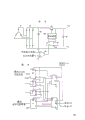
Fig. 1 is the block diagram and the circuit diagram of transmitter that comprises the power amplifier of one embodiment of the present of invention;
Fig. 2 is the circuit diagram of a level of amplifier shown in Figure 1;
Fig. 3 is improved circuit diagram of amplifier and block diagram, thereby wherein different level obtains output voltage with identical amplitude in response to the AC signal with identical amplitude in the different time in the different time;
Fig. 4 is the block diagram that is included in the ring modulator in the amplifier of Fig. 3.
Now, comprise the block diagram and the circuit diagram of the transmitter of the embodiment of the invention referring to Fig. 1.Transmitter comprises high-power output stage 11, the latter comprises tetrode 12, antenna coupling network 13, screen supply 14, dc bias source 15 and radio-frequency carrier source 16 are selected bias generator 15 and carrier source 16 to make tetrode be driven like this and are worked in category-B, C class or G class state.Carrying as the tetrode anode by the modulation source that comprises modulator 17 is the modulation voltage of the supply voltage of plate.In fact, modulator 17 is that response ac modulation source 18(typical source is audio frequency, the source speech signal that changes between zero voltage level and predetermined maximum level) high power amplifier.Tetrode 12 response sources 15 and 16 output, the voltage of power supply 14 and the variable amplitude direct voltage that is applied to its plate 11, to produce the amplitude-modulated wave that centre frequency equals the frequency of carrier source 16, the amplitude-modulated wave that tetrode 12 obtains flows to antenna 19 by antenna coupling network 13.
Power amplifier 17 produces the variable amplitude of the reproduction that is the ripple that produced by voltage source 18 basically, the ripple of variable frequency, and still, the ripple that is produced by amplifier 17 has the stepped change of discrete voltage levels, and typical stepped change approximately is 600 volts.In one embodiment, between minimum that is obtained by amplifier 17 and the maximum voltage 48 different ladders are arranged, so maximum voltage approximately is 28800 volts, power level is 500 kilowatts.When the output of amplifier 17 is fed to the plate of tetrode 12, to its filtering or ask its mean value, make that the tetrode plate voltage is the accurate reproduction of the ripple in source 18 with low pass filter 21.
In one embodiment, power amplifier 17 comprises 48 different levels 34.1,34.2,34.3 ... 34.46,34.47 and 34.48, for simplicity, preceding two and latter two level, i.e. level 34.1,34.2,34.47 and 34.48 only are shown.The same parts of each same stages has the identical label in decimal point left side, and has the same numeral that equals progression on the decimal point right side with the parts of one-level.Below describe level 34.1 in detail, because all levels 34 are all identical, it is in general enough that all levels are discussed level 34.1.The number of level can be greater than or less than 48, but several levels under any circumstance should be arranged at least.
By output voltage addition with each grade, just be added in together from the response of all grades 34, and the output voltage addition to be the voltage of the output by each grade that superpose realize.
Level each level work of 34 in complete conducting, be saturation condition or nonconducting state, each level with DC power supply driving stage 34 with same electrical pressure, when each level is in complete conducting (saturated) state, the direct voltage that is applied to this grade is sent to the output 41 and 42 of level, when certain one-level of level 34 was ended, output voltage of this grade and output impedance almost reduced to zero.
Therefore output 41 and 42 cascade between the input of ground and low pass filter 21, holds 41.1 ground connection, and end 42.1 and 41.2 connects together, and end 42.47 and 41.48 also connects together, and holds 42.48 to receive filter 21.Outputs 41 that produce at end 42.48 and 42 voltage and be fed to low pass filter 21 as the variable amplitude direct voltage like this.
The direct current of each grade of level 34 obtains from three-phase alternating-current supply 51.The elementary winding 52 and 53 that power supply 51 starting and line transformer 54 are connected with 55 △, the three-phase secondary winding 56.1-56.24 that the independent Y of winding 52 startings connects, and transformer 53 startings are similarly the secondary winding 56.25-56.48 of Y connection.Elementary winding 52 and 53 comprises the tap (not shown) of such adjustment, alternating current of each grade of feasible inflow level 34 and the basic homophase of voltage that produces at the ac input end two ends of this grade, in other words, the power factor (PF) of the power that provides to each grade of level 34 during in this grade conducting near 1, so that raise the efficiency, for this reason, the tap of adjusting winding 52 and the 53 like this electric current that make to flow into elementary winding is with respect to have an appointment 30 ° phase shift of the electric current that obtains from secondary winding 56.1-56.48.Because will be approximately be closely coupled to a three-phase primary windings all difficulties are arranged, so be provided with two elementary windings 52 and 53 more than 24 three-phase secondary winding.Each level of level 34 comprises all-wave three-phase rectifier (not shown), has the quite little ripple and the direct voltage of constant amplitude so that three-phase input that will this level converts to.
Each level with the parallel starting level 34 of the output in ac modulation source 18, each grade of level 34 has different threshold values to the output-voltage levels of modulation source 18, set up different threshold values by between the positive direct-current voltages of terminal 62 and ground, connecting resistive voltage divider 61, voltage divider 61 comprises the different taps 65 of each grade of level 34, substitutional resistance 63 is connected between the adjacent tap, and the voltage difference between the adjacent taps is equated.In one embodiment, the voltage in source 62 is 4.8 volts, so tap 65.1,65.2 ... 65.47 and 65.48 voltage is respectively 0,0.1 ... 4.7 and 4.8 volts.
Tap 65 by voltage divider 61 imposes on the threshold value of level 34 and compares with the voltage on the lead 64, when the threshold value of certain one-level of level 34 when imposing on the voltage of this grade by the voltage on the lead 64, this grade is the saturation condition of complete conducting; When the threshold value that provides to certain one-level by voltage divider 61 when being applied to the voltage of this grade by lead 64, this level is in cut-off state.
Level 34.1 is received the earth tap of voltage divider 61, so when the voltage on the lead 64 surpasses null (most of the time all is like this), level 34.1 is with regard to conducting.Impose on the maximum voltage that level 34.48 voltage equals voltage source 18 at terminal 62,34.48 of levels are driven to the saturation condition of complete conducting in the sub-fraction of amplifier in the operating time.In the embodiment that is discussed, level 34.1 except that the voltage in source 18 less than 0.05 volt if having time in all conductings; 34.48 voltages in source 18 of level surpass just conducting fully in 4.75 volts time; When the voltage in source 18 equals 0.0 or 4.8 volt, the level 34.1 and 34.48 each have 50% duty ratio respectively; When the voltage in source 18 is being slightly larger than 0.05 volt and be slightly less than when changing between the 4.75V, the centre of level 34 is at different levels, i.e. level 34.2-34.47 is in complete conducting and cut-off state in the variable time of the function of the amplitude that is essentially source 18.Along with the amplitude in source 18 increases and reduces, the number of the level of conducting also increases and reduces fully, thus fully conducting grade number be the linear function of source 18 amplitudes basically.
Level each amplitude of 34 as audio-source 18, by voltage divider 61 be applied to the threshold voltage of certain one-level and in each cycle in source 18, repeatedly change simultaneously effectively all threshold values at different levels the factor function and work in complete conducting and cut-off state, the variation of effective threshold level of each grade 34 is in the threshold value that should equal at least on the total amount between adjacent level.
In the structure of an equipment that has been constituted by reality, changes of threshold equals poor between the adjacent threshold value, it is found that for the situation that can take place that such variation has reduced the distortion of modulation voltage that is transported to the plate of tetrode 12 by low pass filter 21 widely with respect to there not being variable thresholding.As long as changes of threshold is the sub-fraction of the maximum voltage in source 18, can also make changes of threshold equal threshold value more than a level.If changes of threshold is the twice of the threshold value between the adjacent a pair of level 34, the output of two levels will have been eliminated control problem to the voltage of tap 65 by mean deviation.
Level 34 variable thresholding can obtain by in adding network 72 linear combination being carried out in the output in the output of triangular wave signal source 71 and source 18, the low-limit frequency of triangular wave signal source 71 is the twice of the highest frequency in source 18 at least, preferably its several times, the output maximum voltage amplitude of triangular wave signal source 71 is steady state values with the quite little percentage of maximum amplitude in source 18.Because source 71 has changed the threshold value of each grade of level 34 effectively, the maximum voltage amplitude of the ripple that is obtained by source 71 equals the threshold difference of adjacent a pair of level 34 at least.
Signal source 71 is triangular wave or linear saw-tooth wave preferably, so that the best linearity is provided in the signal of the plate that is coupled to tetrode 12 by low pass filter 21 and reduces distortion, the reason that the linearity obtains is that the ON time of each output stage 34 of being switched on is directly proportional with the instantaneous amplitude of the voltage in source 18, and therefore being switched on grades 34 is that pulsewidth is modulated.Though source 71 preferably has linear change, other waveform also can be used as this source, and for example, in some cases, source 71 can be sinusoidal wave.
The linearity that strengthens can be by coming the frequency in change source 71 to obtain by the output amplitude in source 18 and the function of frequency, along with the frequency and the amplitude increase in source 18, the also corresponding increase of the frequency in source 71.For this purpose, the output in source 18 is coupled to the input in source 71.But, be appreciated that source 71 also can be and the irrelevant constant frequency signal source of the output in source 18.
In a most preferred embodiment, source 71 is with aforesaid U.S. Patent 4,896,372 mode shown in Figure 6 is constructed, in this example, 71 variable frequencies that obtain, the triangle wave frequency of constant amplitude increase and reduce by the function of the similar RMS of the amplitude in source 18 from the source, and in addition, the frequency that source 71 triangular waves are exported correspondingly increases and reduces along with the increase of the frequency in source 18 and minimizing.For this purpose, triangular wave signal source that discloses among Fig. 6 of triangular wave signal source 71 and aforementioned 4,896, No. 372 patents and the element that is connected to its input are the same.
Secondly owing to the control in reason recited above and source 71, when an a specific order 34 was in conducting state, its duration mainly was linearly related to the instantaneous amplitude in source 18, with the RMS amplitude and the frequency dependence in source 18.The output voltage response source 18 of certain one-level 34 changes in zero volt and transformation between 600 volts, and the voltage in source 18 changes between the peak-to-peak value of the middle threshold value of certain one-level and triangular wave signal source 71.Add deduct between the peak-to-peak value in source 71 as long as the amplitude in source 18 is the middle threshold values at this grade, the width of 600 volts of voltage levels that certain one-level obtained just with the amplitude linear correlation in source 18.
Like this, certain one-level 34 just obtains the pwm voltage in zero volt and variation between 600 volts.The mean value of pulse and source 18 are with respect to the ratio that is varied to of the middle threshold value of certain one-level.The pulse width modulated wave that is obtained by level 34.K is superimposed on a grade 34.1-34.(K-1) the summations of 600 volts outputs on, so the output of average filter 21 is high voltage reproductions of the variation in source 18.
Amplitude increase and minimizing along with source 18, also increased gradually for level 34 the number of complete conducting state by starting and reduce, for example, the add circuit 72 of a transient state output level (this level is half of voltage on the terminal 62) is derived in response, half of all grades of amplifier 17 (i.e. level 34.1-35.24) is in conducting state, and remaining level (i.e. level 34.25-34.48) is in nonconducting state.
According to the above, the voltage of output 42.48 is the high voltage staircase waveforms with 48 possibility ladders, when voltage is in any ladder, just obtains the variable-length pulse with a ladder amplitude.To certain one-level of level 34, in threshold interval, the instantaneous amplitude linear correlation in the width of pulse and source 18.Because every grade of effective changes of threshold that is provided by 71 pairs of levels 34 of triangular wave signal source, so the mean value of the staircase waveform of output 42.48 accurately the amplitude of tracing source 18 change, the accurate high voltage that low pass average filter 21 has obtained the waveform in source 18 thus reproduces, and does not have and switching losses that high voltage source interrelates of switching.
The circuit diagram of the most preferred embodiment of each grade of level 34 as shown in Figure 2.The three-phase rectifier 101 that is converted to direct voltage by the three-phase alternating voltage with secondary winding 56 places of transformer 54 or 55 provides direct current to each level of level 34, rectifier 101 is enabled in the shunt capacitor 102 that its two ends produce 600 volts of direct voltages, the voltage at capacitor 102 two ends is connected to output 41 and 42 selectively through the emitting stage-collector access of independent control utmost point bipolar transistor 103, also can use other similar device.Transistor 103 has bipolar emitter-collector characteristic and the high impedance control utmost point feature that is similar to mos field effect transistor.Transistor 103 comprises the collector and emitter of the negative electrode of electrode being connected respectively to capacitor 102 and diode 104, and the anode of diode 104 is received another utmost point of capacitor 102, and diode 104 cross-over connections are in output 41 and 42.
The control utmost point and the control of the bias voltage between the emitting stage at transistor 103 are provided by circuit 105, emitter-the collector access of circuit 105 conversioning transistor 103 between saturated and not conducting, in saturation condition, the direct voltage at capacitor 102 two ends is coupled to output 41 and 42, makes diode 104 partially anti-; When transistor 103 not conductings, the voltage between the output 41 and 42 is owing to reduce to zero rapidly via the quite low impedance that anode and negative electrode provided of diode 104.Therefore, the impedance between the output 41 and 42 remains on first and gives fixed steady state value when transistor 103 is in conducting state, and protects second quite low predetermined value when not conducting of transistor.
Circuit 105 is by comprising that the light-electric pathway of photodiode 106 that is connected to the input of circuit 105 through current-limiting resistance 107 controls, to light-emitting diode 108, the latter is through the output of resistance 111 connections with response comparator 109 by optical coupling (for example by the optical fiber light path) for diode 106.
When comparator 109 output zero levels, diode 108 is activated and makes light-emitting diode 106 luminous, and when comparator 109 outputs 1 level, diode 108 provides no light signal.When diode 106 was luminous, circuit 105 was activated and makes transistor 103 be in saturation condition, then transistor 103 not conductings when not having light to occur on the diode 106.Gone to control the conducting state of the switch of the level 32 that includes transistor 103 by linear combination from the voltage of adding network 72 and bias network 61.
According to a further aspect of the present invention (being shown in Fig. 3 and Fig. 4), a certain input voltage cause different levels 34 be activated with derive identical output voltage and, like in the embodiment in figure 1 for this voltage provided like that.Which grade conducting of selecting level 34 be with AC modulation source 18 before variation with and instantaneous value relevant, with regard to this point, because the variation of modulation source 18 is at random, so the selection of which grade conducting of level 34 also is at random.By making level 34 conducting randomization, when some level in fact never during consumed energy, other level is wastage in bulk or weight energy not also.Therefore, between different levels 34, the distribution of its energy is near equating, so as in level 34 consumed energy in fact balancedly, prevent from certain one-level, to produce superheating phenomenon, this is just in time opposite with Fig. 1, in Fig. 1, almost conducting always of lowest number level (just level 34.1,34.2 etc.), and in fact never conducting of the highest numbering level (just level 34.48,34.47 etc.).The other difference of the amplifier of Fig. 1 and Fig. 3 is: each grade of the level 34 among Fig. 3 modulated at interval in the enterprising horizontal pulse of the frequency of triangle wave source 71.Level 34 the number that is in conducting state at a special time is that the amplitude by signal source 18 is determined.
For this reason, the voltage in source 18 to 71 in adding network 72 by linear combination, and the voltage in the tap 65 in comparator 109.1-109.48 and in voltage divider 61 compares, comparator 109.1-109.48 derives binary-level, and its derivation mode is identical with the mode of corresponding comparator 109 derivation binary-levels among Fig. 1 middle rank 34.1-34.48.
For which level of controlling among the output stage 34.1-34.48 by the function of the current of modulation source 18 and value in the past is in conducting and nonconducting state, the number that will be in the comparator 109.1-109.48 of binary one state compares with number in the output stage 34 of conducting state.This device is such, and for example, if the amplitude in source 18 remains unchanged, the number that then is in the output stage 34 of starting state also keeps certain; But although in fact the amplitude in source 18 is constant, it then is constantly to change which level in the output stage 34 is activated.For example, if the voltage in source 18 is half of voltage on the end points 62, then 24 levels among 48 level 34.1-34.48 are conductings, and during some moment, the voltage when source 18 is a half of the voltage on the end points 62, then level 34.7-34.30 may be switched on, and after the moment during, a level 34.8-34.31 may be switched on, but during two moment, the voltage of deriving by level 34 and 24 * 600=14 always, 400 volts.
For this reason, the number that provides the comparator 109.1-109.48 of binary one level is to offer adding network 121 by the binary one level with these comparators to point out, the output voltage of this adding network 121 is direct voltages that have one of 48 probable values at any time, and each the possible output voltage in the adder 121 represents to have among the comparator 109.1-109.48 number of the comparator of binary one level.
In each cycle of triangle wave source 71, the output of comparator 109.1-109.48 is repeatedly sampled by being fed to sampling and maintenance (promptly latching) network 122.1-122.48 respectively, and this network is also in response to the clock source 123 with several mhz frequencys.The output of latching of latch 122.1-122.48 is sent to adding network 121, and when occurring changing in modulation source 18 and the wave source 71, the output level of add circuit 121 correspondingly changes.
The output signal of adder 121 and an expression are in the signal (deriving from adder 125) of number of the level 34 of fully conducting state and compare, adder 125 is in response to latching network 133.1-133.48, and the latter is respectively in response to ring-type modulator 127 and clock 123 and 48 different binary conditions.Adder 125 provides the output with one of 48 varying levels, and each level of these 48 varying levels shows conducting and the nonconducting state of grade 34.1-34.48. Adder 121 and 125 output signal are fed to comparator 126, and comparator 126 provides selectively as two forwards (being Binary Zero to 1) break-in of the function of the output signal of adder 121 and 125 and shifts.
Be used in which level that the transition on the output of comparator 126 controls among the output stage 34.1-34.48 and be in conducting state and nonconducting state, for this reason, the output of comparator 126 is fed to two separated inputs of ring-type modulator 127, and this ring-type modulator is also in response to clock source 123.Ring-type modulator 127 includes 48 outputs, and each end is corresponding to the level of output stage 34.1-34.8.The number that is in the output stage 34 of conducting state is generally equal to the number that has the comparator of binary one level among the comparator 109.1-109.48, but which has the binary one level and there is no other concord between this among which grade conducting and the comparator 109.1-109.48 in the level 34.
Ring-type modulator 127 includes 128.1-128.48 and two groups of exit points of 129.1-129.48, and parallel respectively is that abundant conducting and non-conduction binary signal drive by which level among the expression 34.1-34.48.Signal on exit point 128.1-128.48 is used as control input and is fed to a grade 34.1-34.48, and these controls comprise optical fiber communication, as the front according to Fig. 1 and Fig. 2 described.Signal on output 128.1-128.48 is fed to latch 133.1-133.48 as input, is fed to adder 125 then.
The most preferred embodiment of ring-type modulator 127 is described in detail in Fig. 4, and it includes recirculation shift register 131 and 132 and 48 output latch 133.1-133.48 of two 48 grades, and each constitutes a J-K flip flop.Each shift register 131 and 132 all comprises increment (INC) input and the input end of clock of exporting separately in response to clock source 123 in response to comparator network 126. Shift register 131 and 132 only is driven on a positive direction, thereby when response was fed to the transition of this increment input, the shift register stage that is in the binary one state moved forward 1.A specific time, having only certain one-level in the shift register 131 and 132 is to be in a binary one state.When a binary one state was afterbody (i.e. level 48) in each shift register 131 and 132, the next positive change that occurs on the increment input of this shift register of response shifted, and the binary one state of shift register is advanced to level 1.During the forward transition of clock 123, when the instantaneous of a forward transition appears in the increment input of shift register, 1 of shift register 131 and 132 state reach.
For each of the latch 133.1-133.48 of each grade setting of level 34.1-34.48 includes a set (S) and reset (R) input and an input end of clock, the clock input of latch 133.1-133.48 is to provide by the output in clock source 123 is parallel.The set of latch 133.1-133.48 input is connected respectively to the exit point of each grade among the level 1-48 of shift register 132, and the input that resets of latch 133.1-133.48 is connected respectively to each exit point of the level 1-48 of shift register 131.When latch was set (promptly at the binary one state), the output of latch 133.1-133.48 provided the binary one level to exit point 127.1-127.48 and 128.1-128.48.
Each latch 133.1-133.48 is such one type, and promptly during the clock pulse input in front, response is fed to the Binary Zero state of the RESET input, described latch, and promptly trigger is in the Binary Zero state; And during the input of clock pulse in front, in response to the binary one state that is fed to set input, then latch 133.1-133.48 is in the binary one state.If in a specific clock interval, a binary one is fed to resetting and set input of a specific latch 133.1-133.48, then the output state of this specific trigger is returned to opposite binary condition, promptly changes to 0 or change to 1 from 0 from 1.Only just appearance during the positive-going transition of the clock 123 after and then transition of the variation of this state of latch 133.1-133.48 at the Binary Zero to 1 of the set of certain triggers or the RESET input.
When each latch 133.1-133.48 was in the initial reset state, general reset circuit (not shown) was activated shift register 131 and 132, thereby level 1 initial set is a binary one state.
At work, have the shift register 131 of binary one value and 132 level and show usually that in the scope of output stage 34 which level is respectively reset stage and is the set level, shift register 131 and these levels of 132 are expressed as N(r respectively) and N(s).If N(s) greater than N(r), output stage 34.N(r+1 then) to 34.N(s) be conducting, output stage 34.1 is to 13.N(r simultaneously) and 34.N(s+1) be non-conduction to 34.48; If N(r) greater than N(s), output stage 34.N(r then) to 34.N(s-1) be non-conduction, output stage 34.1 is to 34.N(r-1 simultaneously) and 34.N(s) are conductings to 34.48; If N(r) equal N(s), then output stage 34.1 to 34.48 or all conducting or not conducting.
Compare with number in comparator 126 by the number of the indicated output stage that is in conducting state 34 of the output of adder 121 by the represented output stage that is in conducting state 34 of the output of adder 125.In the one-period of clock 123, when the difference of the output of the output of adder 121 and adder 125 during, then in the count increments 1 of this clock time internal shift register 132 greater than work dead band from-Vref to+Vref; On the contrary, in the one-period of clock 123, when the output of adder 125 surpasses the output of adder 121, the count increments 1 of shift register 131.Owing to the state of shift register 131 and 132 only is incremented in response to the transition of the output of comparator 126, described comparator itself again response source 18 with respect to by the variation of the set threshold value of voltage divider 61 and the variation of triangle wave source 71, therefore, in response to the amplitude of the output of adder 72, N(s) and N(r) correlation corresponding to changing by network 61 determined threshold values.Therefore, which level 34 conducting is to change on a compatible basis, thereby prevents the lasting loss in the level of lowest number, and the situation that amplifier had of like Fig. 1 is such.In fact, level each grade of 34 has different threshold values, and this threshold value is with N(r) and numerical value N(s) change.
At the input of filter 21, the transition of the amplitude of level 34 output voltage sum response triangle wave source 71 respective sources 18 0 and 600V between conversion.Time between these conversions is to be controlled by the amplitude in source 18, but, not at the same level 34 enter conducting state in response to the variation of triangle wave source 71 in the different time, and therefore, the actual power that is dissipated on the different output stages 34 is divided equally by these grades.
As long as the voltage in ac modulation source 18 keeps constant on the little voltage of ratio voltage relevant with the one-level threshold value, have only the one-level of output stage 34.1-34.48 to enter conducting state in some moment so.The conduction duration of a specific conducting level is determined by the amplitude in source 18.On a determined frequency of the frequency by source 71, all levels of level 34.1-34.48 enter conducting state in succession.The inversion frequency of a specific output stage 34 is substantially equal to the frequency in source 71 divided by output progression, and its representative value is about 2KHZ, and the transition loss of each output stage is just relatively low like this.Along with the variation of the voltage in source 18, also correspondingly change at the number of the output stage 34 of a conducting state, the conduction interval of a level of this output stage also will change.Which output stage 34 is in conducting state, and this current and former numerical value with ac modulation source 18 is relevant.
The voltage of removing source 18 is (here this source voltage is lower than the threshold voltage of the one-level of level 34) outside the low-down situation, under actual all situations, the difference that is loaded into the shift register 131 of binary one level and 132 progression is greater than 1, this makes has more than one latch 133.1-133.48 to enter the binary one state at synchronization, therefore, more than one output stage 34.1-34.48 is entered conducting state by startup simultaneously usually.The duty ratio of each conducting output stage 34 is that the amplitude by the voltage in source 18 decides.
Though here several specific embodiments of the present invention are described and graphic extension, are not violating under the prerequisite of the correct spirit and scope of the present invention of defined in the claims and can make further modification to this embodiment.For example, power amplifier of the present invention is except that also can be used for other purpose as the radio transmitter.If the bigger distortion of being followed is permissible words, then triangle wave source 71 can remove from the circuit of Fig. 2 and Fig. 3.
Claims (27)
1, an amplifier in response to a signal source, comprise that several are activated the level that becomes two states in two level states at least, control for this state of each grade is relevant above a threshold value with the value of this signal source, each grade has a different threshold value, said each threshold value and signal source configuration make when the value of signal source changes with respect to threshold value not at the same level, each level changes between said pair of level state, the two level outputs relevant with two level states of a plurality of grades are added, and it is characterized in that: use the value little with respect to the predetermined maximum of signal source to change the device of threshold value continuously.
2, a kind of in response to the amplifier that allows to have as a signal source of the changing value of the function of time, comprise that several are activated the level that becomes two states in two level states at least, control for this state of each grade is relevant above a threshold value with the value of this signal source, the configuration of described each threshold value and signal source makes when the value of signal source changes with respect to threshold value not at the same level, each level changes between said pair of level state, it is characterized in that: continuously change the device of threshold value with respect to a middle threshold value, its change amount is the function of the value of signal source.
3, one in response to having a N+K value and allowing to have amplifier as a signal source of the changing value of the function of time, comprise that several are activated the level that becomes two states in different two level states at least, the two level outputs that are relevant to two level states of a plurality of grades are added to obtain the summation response, it is characterized in that: start at different levels so that to be in the one-level at least that is proportional in N and these grades of number of the level of one of said state be the device of pulse-width modulation in response to described signal source, the duty ratio of this pulse-width modulation is proportional to K makes the mean value of the summation response in the one-period of this pulse-width modulation response be proportional to N+K, one of any pulse-width modulation that allows to be proportional to K of said level.
4, one in response to an amplifier that allows to have as the signal source of the changing value of the function of time, comprise several levels that are started as a state in the two level states of two differences at least, two level outputs corresponding to two level states of a plurality of grades are added to obtain the summation response for the piecewise function of this signal source, it is characterized in that: start at different levels in response to signal source so that be in number and the value of signal source and the proportional device of combination of a value with continuous variable signal little with respect to the predetermined maximum of signal source of the level of one of said state.
5, as claim 2 or 3 or 4 described amplifiers, it is characterized in that wherein each said level has a different middle threshold value, when changing with respect to the threshold value of certain one-level with the value of convenient signal source, the state of this grade changes.
6, amplifier as claimed in claim 5 is characterized in that further comprising the device of using the value little with respect to the predetermined maximum of signal source to change the threshold value of each grade continuously.
7, as claim 1 or 2 or 5 or 6 described amplifiers, the threshold value that it is characterized in that different described levels changes, so that when the value of signal source does not change, different levels are in described first and second states in the different time, and for the value of identical signal source derive identical and.
8, as claim 1 or 2 or 5 or 6 described amplifiers, it is characterized in that wherein a plurality of grades threshold value is to be provided by the control circuit in response to DC reference voltage, this reference voltage is to be supplied with by the voltage divider of the end points that is connected across DC power supply, this voltage divider includes several at least taps, and the voltage in each tap is corresponding to every grade threshold value.
9, as claim 1 or 2 or 6 described amplifiers, it is characterized in that wherein a plurality of grades threshold value is to be provided by the control circuit in response to DC reference voltage, this reference voltage is to be supplied with by the voltage divider that is connected across the DC power supply end points, this voltage divider comprises several at least taps, each level includes a comparator, this comparator is in response to the value of following combination (a) signal source, (b) represent the amplitude of the signal of changing value, (c) reference value of being controlled by the voltage in the tap is so that produce the transition output signal of the conducting state with the controlled stage of being used for.
10, one in response to an amplifier that allows to have as the signal source of the changing value of the function of time, comprise several at least levels that become two states in different two level states that are activated, being added so that obtains corresponding to the two level output of two level states of a plurality of grades is that the summation of piecewise function of signal source responds; Value in response to signal source produces the devices that the number that shows the level that is in one of described state respectively is first and second instructions of increase and minimizing; It is characterized in that: respond the number that above-mentioned instruction (a) increase and minimizing obtain the output stage of said first and second level, make that obtain the longest level response second instruction of first level time is activated and obtains the longest level response second instruction of second level time to obtain second level and be activated obtaining first level, even and (b) the value no change of signal source also order about levels different in different time and obtain the device that first level and different levels obtain second level.
11, in response to an amplifier that allows to have as the signal source of the changing value of the function of time, comprise that several are activated one the level that becomes in two different two level states at least, being added so that obtains corresponding to the two level output of two level states of a plurality of grades is that the summation of piecewise function of signal source responds; In response to second device of indicating of signal source with the number of first indication of the number of the level that obtains first state that to be in and the actual level that is in first state; And be used for controlling the device of number that each said level is in the time span of said first state and is in the level of said first state according to the comparative results of first and second indications; It is characterized in that: described control device comprises and is used to store a device with the proportional value of number of the level that is in two level states, according to showing that first indication surpasses second indication and second and indicates the comparative result that surpasses first indication, the value that is stored in the storing apparatus changes.
12, amplifier as claimed in claim 11 is even is characterized in that the described device that is used to control also orders about in the different time different levels and obtains first level state and obtain second level state with different levels when the value of signal source does not change.
13, as claim 11 or 12 described amplifiers, it is characterized in that being used for obtaining first device of indicating comprises a plurality of input units that have only two level outputs, the two level outputs of value control according to the signal source of a threshold value that surpasses each input unit, each input unit has different threshold values, threshold value and signal source are set like this to make when the value of signal source during with respect to the changes of threshold of different input stages, the output of input unit changes between described pair of level output, and the output of input unit is added together.
14, amplifier as claimed in claim 13 is characterized in that further comprising the device of using the value little with respect to the predetermined maximum of signal source to change threshold value continuously.
15, amplifier as claimed in claim 14, the device that it is characterized in that being used for changing the state of a said level comprise the response comparative result increase and reduce first state that is in grade number.
16, amplifier as claimed in claim 15, it is characterized in that the device that stores comprises a ring-type modulator with a plurality of grades, this ring-type modulator comprises a pair of shift register, each shift register has one and increases progressively input and a plurality of state, each state is relevant with a level, a response that increases progressively in the input shows the signal of first indication greater than second indication, and other increases progressively the input response and shows the signal of second indication greater than first indication.
17, any one described amplifier of claim as described above is characterized in that amplifier is a power amplifier, and each grade is the power output stage of this power amplifier.
18, as claim 1 or 2 or 3 or 4 or 5 or 6 or 8 or 9 described amplifiers, it is characterized in that amplifier is included in the control circuit of power output stage of power amplifier, power output stage only is activated and becomes to have electric current and no current state; And comprise according to the summation of the outputs at different levels of control circuit and control the device which power output stage is in has electric current and no current state and power output stage to be in the length of the time that electric current and no current state are arranged.
19, amplifier as claimed in claim 18 is characterized in that starting to control that the device of making usefulness starts output stage so that for the value of identical signal source, different output stages be have electric current with currentless.
20, amplifier as claimed in claim 18 starts output stage so that when the value of signal source does not change even it is characterized in that starting to control the device of making usefulness, different output stages the different moment be have electric current with currentless.
21, as claim 1 or 2 or 4 or 7 or be subordinated to the amplifier described in any one claim of aforesaid right requirement, it is characterized in that wherein " variation " is to be provided by a signal with a constant variation value.
22, amplifier as claimed in claim 21 is characterized in that the signal with a constant variation value has a fixing frequency.
23, amplifier as claimed in claim 21, the signal that it is characterized in that having a constant variation value is a ripple with variable frequency, this variable frequency depends on a parameter of described signal source.
24, amplifier as claimed in claim 23 is characterized in that described parameter is an amplitude.
25, amplifier as claimed in claim 23 is characterized in that described parameter is a frequency.
26, amplifier as claimed in claim 23, the signal that it is characterized in that having a constant variation value is a ripple with a variable frequency, this variable frequency depends on the amplitude and the frequency of described signal source.
27,, it is characterized in that the signal with a constant variation value represents a ripple that has as the linear change of the function of time as any one described amplifier of claim 21-26.
Applications Claiming Priority (2)
| Application Number | Priority Date | Filing Date | Title |
|---|---|---|---|
| US07/533,646 US5099203A (en) | 1990-06-05 | 1990-06-05 | Power amplifier having multiple switched stages and method of operating same |
| US533,646 | 1990-06-05 |
Publications (2)
| Publication Number | Publication Date |
|---|---|
| CN1058496A CN1058496A (en) | 1992-02-05 |
| CN1023174C true CN1023174C (en) | 1993-12-15 |
Family
ID=24126870
Family Applications (1)
| Application Number | Title | Priority Date | Filing Date |
|---|---|---|---|
| CN91104560A Expired - Fee Related CN1023174C (en) | 1990-06-05 | 1991-06-04 | Power amplifier having multiple switched stages |
Country Status (7)
| Country | Link |
|---|---|
| US (1) | US5099203A (en) |
| EP (3) | EP0651501B1 (en) |
| CN (1) | CN1023174C (en) |
| CA (1) | CA2043838C (en) |
| DE (3) | DE69131242T2 (en) |
| ES (2) | ES2032739T3 (en) |
| IL (1) | IL98244A (en) |
Families Citing this family (64)
| Publication number | Priority date | Publication date | Assignee | Title |
|---|---|---|---|---|
| US5099203A (en) | 1990-06-05 | 1992-03-24 | Continental Electronics Corporation | Power amplifier having multiple switched stages and method of operating same |
| US5200707A (en) * | 1990-06-05 | 1993-04-06 | Continental Electronics Corporation | Amplifier with multiple switched stages and noise suppression |
| US5345198A (en) * | 1993-06-10 | 1994-09-06 | Crown International, Inc. | Power supply modulator circuit for transmitter |
| ES2168311T3 (en) * | 1993-06-10 | 2002-06-16 | Crown Internat Inc | POWER MODULATOR CIRCUIT FOR TRANSMITTERS. |
| CN1061491C (en) * | 1994-09-02 | 2001-01-31 | 王冠国际公司 | Power supply modulator circuit for transmitter |
| CN1319269C (en) * | 2000-09-21 | 2007-05-30 | 皇家菲利浦电子有限公司 | Switching power amplifier |
| US6653898B2 (en) | 2000-12-28 | 2003-11-25 | Samsung Electronics Co., Ltd. | High efficiency stage-switching CDMA power amplifier |
| US20020163984A1 (en) * | 2001-05-03 | 2002-11-07 | Katzman Vladimir V. | Clock and data recovery unit based on class B amplifier |
| AU2002347511A1 (en) | 2001-12-17 | 2003-06-30 | Koninklijke Philips Electronics N.V. | Isolated converter with synchronized switching leg |
| US6803821B1 (en) * | 2003-04-03 | 2004-10-12 | Fairchild Semiconductor Corporation | Switchable amplifier circuit having reduced shutdown current |
| JP2005109614A (en) * | 2003-09-29 | 2005-04-21 | Sanyo Electric Co Ltd | Receiver |
| US7664520B2 (en) * | 2004-06-24 | 2010-02-16 | Nokia Corporation | Low current direct conversion transmitter architecture |
| US9112452B1 (en) | 2009-07-14 | 2015-08-18 | Rf Micro Devices, Inc. | High-efficiency power supply for a modulated load |
| EP2561611B1 (en) | 2010-04-19 | 2015-01-14 | RF Micro Devices, Inc. | Pseudo-envelope following power management system |
| US9099961B2 (en) | 2010-04-19 | 2015-08-04 | Rf Micro Devices, Inc. | Output impedance compensation of a pseudo-envelope follower power management system |
| US9431974B2 (en) | 2010-04-19 | 2016-08-30 | Qorvo Us, Inc. | Pseudo-envelope following feedback delay compensation |
| US8981848B2 (en) | 2010-04-19 | 2015-03-17 | Rf Micro Devices, Inc. | Programmable delay circuitry |
| US9954436B2 (en) | 2010-09-29 | 2018-04-24 | Qorvo Us, Inc. | Single μC-buckboost converter with multiple regulated supply outputs |
| WO2012068258A2 (en) | 2010-11-16 | 2012-05-24 | Rf Micro Devices, Inc. | Digital fast cordic for envelope tracking generation |
| WO2012109227A2 (en) | 2011-02-07 | 2012-08-16 | Rf Micro Devices, Inc. | Group delay calibration method for power amplifier envelope tracking |
| US9246460B2 (en) | 2011-05-05 | 2016-01-26 | Rf Micro Devices, Inc. | Power management architecture for modulated and constant supply operation |
| US9379667B2 (en) * | 2011-05-05 | 2016-06-28 | Rf Micro Devices, Inc. | Multiple power supply input parallel amplifier based envelope tracking |
| US9247496B2 (en) | 2011-05-05 | 2016-01-26 | Rf Micro Devices, Inc. | Power loop control based envelope tracking |
| WO2012166992A1 (en) | 2011-05-31 | 2012-12-06 | Rf Micro Devices, Inc. | Rugged iq receiver based rf gain measurements |
| US9019011B2 (en) | 2011-06-01 | 2015-04-28 | Rf Micro Devices, Inc. | Method of power amplifier calibration for an envelope tracking system |
| US8952710B2 (en) | 2011-07-15 | 2015-02-10 | Rf Micro Devices, Inc. | Pulsed behavior modeling with steady state average conditions |
| US9263996B2 (en) | 2011-07-20 | 2016-02-16 | Rf Micro Devices, Inc. | Quasi iso-gain supply voltage function for envelope tracking systems |
| US8942652B2 (en) | 2011-09-02 | 2015-01-27 | Rf Micro Devices, Inc. | Split VCC and common VCC power management architecture for envelope tracking |
| US8957728B2 (en) | 2011-10-06 | 2015-02-17 | Rf Micro Devices, Inc. | Combined filter and transconductance amplifier |
| JP5366032B2 (en) * | 2011-10-20 | 2013-12-11 | Tdk株式会社 | Ramp signal generation circuit and ramp signal adjustment circuit |
| WO2013063387A2 (en) | 2011-10-26 | 2013-05-02 | Rf Micro Devices, Inc. | Inductance based parallel amplifier phase compensation |
| US9024688B2 (en) | 2011-10-26 | 2015-05-05 | Rf Micro Devices, Inc. | Dual parallel amplifier based DC-DC converter |
| US9484797B2 (en) | 2011-10-26 | 2016-11-01 | Qorvo Us, Inc. | RF switching converter with ripple correction |
| US9294041B2 (en) | 2011-10-26 | 2016-03-22 | Rf Micro Devices, Inc. | Average frequency control of switcher for envelope tracking |
| AU2011380562B2 (en) * | 2011-11-03 | 2017-04-20 | Hubbell Incorporated | Control system for synchronous capacitor switch |
| US9515621B2 (en) | 2011-11-30 | 2016-12-06 | Qorvo Us, Inc. | Multimode RF amplifier system |
| US8975959B2 (en) | 2011-11-30 | 2015-03-10 | Rf Micro Devices, Inc. | Monotonic conversion of RF power amplifier calibration data |
| US9250643B2 (en) | 2011-11-30 | 2016-02-02 | Rf Micro Devices, Inc. | Using a switching signal delay to reduce noise from a switching power supply |
| US9256234B2 (en) | 2011-12-01 | 2016-02-09 | Rf Micro Devices, Inc. | Voltage offset loop for a switching controller |
| US9280163B2 (en) | 2011-12-01 | 2016-03-08 | Rf Micro Devices, Inc. | Average power tracking controller |
| US8947161B2 (en) | 2011-12-01 | 2015-02-03 | Rf Micro Devices, Inc. | Linear amplifier power supply modulation for envelope tracking |
| US9041365B2 (en) | 2011-12-01 | 2015-05-26 | Rf Micro Devices, Inc. | Multiple mode RF power converter |
| US9494962B2 (en) | 2011-12-02 | 2016-11-15 | Rf Micro Devices, Inc. | Phase reconfigurable switching power supply |
| US9813036B2 (en) | 2011-12-16 | 2017-11-07 | Qorvo Us, Inc. | Dynamic loadline power amplifier with baseband linearization |
| US9298198B2 (en) | 2011-12-28 | 2016-03-29 | Rf Micro Devices, Inc. | Noise reduction for envelope tracking |
| US8981839B2 (en) | 2012-06-11 | 2015-03-17 | Rf Micro Devices, Inc. | Power source multiplexer |
| WO2014018861A1 (en) | 2012-07-26 | 2014-01-30 | Rf Micro Devices, Inc. | Programmable rf notch filter for envelope tracking |
| US9225231B2 (en) | 2012-09-14 | 2015-12-29 | Rf Micro Devices, Inc. | Open loop ripple cancellation circuit in a DC-DC converter |
| US9197256B2 (en) | 2012-10-08 | 2015-11-24 | Rf Micro Devices, Inc. | Reducing effects of RF mixer-based artifact using pre-distortion of an envelope power supply signal |
| WO2014062902A1 (en) | 2012-10-18 | 2014-04-24 | Rf Micro Devices, Inc | Transitioning from envelope tracking to average power tracking |
| US9627975B2 (en) | 2012-11-16 | 2017-04-18 | Qorvo Us, Inc. | Modulated power supply system and method with automatic transition between buck and boost modes |
| US9300252B2 (en) | 2013-01-24 | 2016-03-29 | Rf Micro Devices, Inc. | Communications based adjustments of a parallel amplifier power supply |
| US9178472B2 (en) | 2013-02-08 | 2015-11-03 | Rf Micro Devices, Inc. | Bi-directional power supply signal based linear amplifier |
| WO2014152876A1 (en) | 2013-03-14 | 2014-09-25 | Rf Micro Devices, Inc | Noise conversion gain limited rf power amplifier |
| WO2014152903A2 (en) | 2013-03-14 | 2014-09-25 | Rf Micro Devices, Inc | Envelope tracking power supply voltage dynamic range reduction |
| US9479118B2 (en) | 2013-04-16 | 2016-10-25 | Rf Micro Devices, Inc. | Dual instantaneous envelope tracking |
| US9374005B2 (en) | 2013-08-13 | 2016-06-21 | Rf Micro Devices, Inc. | Expanded range DC-DC converter |
| US9614476B2 (en) | 2014-07-01 | 2017-04-04 | Qorvo Us, Inc. | Group delay calibration of RF envelope tracking |
| US9912297B2 (en) | 2015-07-01 | 2018-03-06 | Qorvo Us, Inc. | Envelope tracking power converter circuitry |
| US9843294B2 (en) | 2015-07-01 | 2017-12-12 | Qorvo Us, Inc. | Dual-mode envelope tracking power converter circuitry |
| US9973147B2 (en) | 2016-05-10 | 2018-05-15 | Qorvo Us, Inc. | Envelope tracking power management circuit |
| CN107343245B (en) * | 2017-08-28 | 2023-12-22 | 东莞精恒电子有限公司 | Pulse width modulation double PWM unit power amplifier module |
| US10476437B2 (en) | 2018-03-15 | 2019-11-12 | Qorvo Us, Inc. | Multimode voltage tracker circuit |
| CN113193844B (en) * | 2021-05-31 | 2022-09-23 | 锐石创芯(深圳)科技股份有限公司 | Push-pull power amplifying circuit |
Family Cites Families (17)
| Publication number | Priority date | Publication date | Assignee | Title |
|---|---|---|---|---|
| US3506920A (en) * | 1966-02-10 | 1970-04-14 | Gates Radio Co | High efficiency transformer utilizing pulse duration modulation to eliminate audio-rf transformer coupling |
| US3588744A (en) * | 1969-11-07 | 1971-06-28 | Gates Radio Co | Amplitude compensated pulse duration modulator |
| US4164714A (en) * | 1977-09-26 | 1979-08-14 | Harris Corporation | Polyphase PDM amplifier |
| US4140980A (en) * | 1978-02-24 | 1979-02-20 | Rockwell International Corporation | Compensation circuit for trailing edge distortion of pulse-width modulated signal |
| GB2064901B (en) * | 1979-11-30 | 1984-11-07 | Harris Corp | Digital high power amplifier |
| US4369409A (en) * | 1980-08-05 | 1983-01-18 | Patelhold Patentverwertungs- & Elektro-Holding A.G. | Low-frequency power amplifier |
| US4468626A (en) * | 1982-01-25 | 1984-08-28 | Harris Corporation | Polyphase PDM amplifier |
| DE3465857D1 (en) * | 1983-05-10 | 1987-10-08 | Bbc Brown Boveri & Cie | Digital power switching amplifier |
| DE3534979A1 (en) * | 1985-07-25 | 1987-01-29 | Licentia Gmbh | POWER SUPPLY |
| US4724420A (en) * | 1985-12-19 | 1988-02-09 | Varian Associates, Inc. | Method and apparatus for quasi-analog reconstructions of amplitude and frequency varying analog input signals |
| US4776036A (en) * | 1986-02-25 | 1988-10-04 | Varian Associates, Inc. | RF-AM transmitter with pulse width modulator |
| US4747161A (en) * | 1986-02-25 | 1988-05-24 | Varian Associates, Inc. | AM-RF transmitter with compensation for power supply variations |
| US4896372A (en) * | 1986-02-25 | 1990-01-23 | Varian Associates, Inc. | Pulse width modulator for AM-RF transmitter |
| US4748421A (en) * | 1987-04-08 | 1988-05-31 | Scs Telecom, Inc. | Enhanced class SM power amplifier |
| US4831334A (en) * | 1987-06-08 | 1989-05-16 | Hughes Aircraft Company | Envelope amplifier |
| DE3805754A1 (en) * | 1988-02-24 | 1989-09-07 | Olympia Aeg | DIGITAL SWITCHING AMPLIFIER |
| US5099203A (en) | 1990-06-05 | 1992-03-24 | Continental Electronics Corporation | Power amplifier having multiple switched stages and method of operating same |
-
1990
- 1990-06-05 US US07/533,646 patent/US5099203A/en not_active Expired - Lifetime
-
1991
- 1991-05-23 IL IL9824491A patent/IL98244A/en active IP Right Grant
- 1991-06-04 EP EP95100838A patent/EP0651501B1/en not_active Revoked
- 1991-06-04 CA CA002043838A patent/CA2043838C/en not_active Expired - Fee Related
- 1991-06-04 ES ES91305053T patent/ES2032739T3/en not_active Expired - Lifetime
- 1991-06-04 DE DE69131242T patent/DE69131242T2/en not_active Expired - Fee Related
- 1991-06-04 EP EP91305053A patent/EP0466322B1/en not_active Expired - Lifetime
- 1991-06-04 DE DE199191305053T patent/DE466322T1/en active Pending
- 1991-06-04 CN CN91104560A patent/CN1023174C/en not_active Expired - Fee Related
- 1991-06-04 DE DE69129340T patent/DE69129340T2/en not_active Expired - Fee Related
- 1991-06-04 ES ES95100838T patent/ES2116626T3/en not_active Expired - Lifetime
- 1991-06-04 EP EP95118442A patent/EP0703662A2/en not_active Withdrawn
Also Published As
| Publication number | Publication date |
|---|---|
| DE69131242D1 (en) | 1999-06-24 |
| EP0651501B1 (en) | 1998-04-29 |
| CA2043838C (en) | 1997-01-21 |
| DE69131242T2 (en) | 1999-11-25 |
| ES2032739T1 (en) | 1993-03-01 |
| EP0651501A3 (en) | 1995-06-07 |
| CN1058496A (en) | 1992-02-05 |
| US5099203A (en) | 1992-03-24 |
| EP0466322A2 (en) | 1992-01-15 |
| EP0651501A2 (en) | 1995-05-03 |
| EP0466322A3 (en) | 1992-05-06 |
| EP0703662A3 (en) | 1996-05-01 |
| EP0703662A2 (en) | 1996-03-27 |
| DE69129340D1 (en) | 1998-06-04 |
| IL98244A (en) | 1996-01-19 |
| DE69129340T2 (en) | 1998-10-15 |
| CA2043838A1 (en) | 1991-12-06 |
| DE466322T1 (en) | 1992-12-17 |
| EP0466322B1 (en) | 1999-05-19 |
| ES2032739T3 (en) | 1999-09-16 |
| IL98244A0 (en) | 1992-06-21 |
| ES2116626T3 (en) | 1998-07-16 |
Similar Documents
| Publication | Publication Date | Title |
|---|---|---|
| CN1023174C (en) | Power amplifier having multiple switched stages | |
| US7525296B2 (en) | Spread spectrum power converter with duty-cycle error compensation | |
| US7304594B2 (en) | Transmitting and receiving device and transmitting device and receiving device | |
| US3413570A (en) | High efficiency rf power amplification with modulation signal controlled "on"-"off" switch varied amplifier dc potentials | |
| CA2604480C (en) | A digital amplitude modulation transmitter with pulse width modulating rf drive | |
| EP1143609A3 (en) | High frequency power amplifier having a bipolar transistor | |
| CN1618168A (en) | Digital PWM input D class amplifier by PMW negative feedback | |
| SE467331B (en) | AUDIO POWER AMPLIFIER WITH PULSE WIDE MODULATION AND AN AUDIO POWER STEP | |
| CN1347589A (en) | Class D digital amplifier | |
| CN1117428C (en) | Method in compensation of unlinearities in amplifier, amplifier, and uses of method and amplifier | |
| KR101041913B1 (en) | Polyphase impedance transformation amplifier | |
| CN111142601B (en) | Digital control hybrid power modulator and modulation circuit | |
| CN107231096B (en) | Primary side feedback switching power supply multi-order loop control circuit | |
| JP2006158110A (en) | Time division control chopper circuit | |
| CN1608343A (en) | Attenuation control for digital power converters | |
| JPS6281804A (en) | Switching amplifier | |
| CN1714501A (en) | Pulse modulated power converter | |
| KR20080089277A (en) | System and method for digital modulation | |
| AU654786B2 (en) | Amplifier with multiple switched stages and noise suppression | |
| US4899116A (en) | Apparatus and method for paralleling power field effect transistors in high frequency amplifiers | |
| Chen et al. | An open-loop digitally controlled supply modulator for wideband envelope tracking | |
| KR102092670B1 (en) | A pulse width control circuit device with the ripple free circuit | |
| CN114244155B (en) | Double-loop control circuit for power supply conversion circuit and high-precision constant-current control method | |
| KR100428241B1 (en) | digital amplifier | |
| RU2007849C1 (en) | Powerful key amplifier |
Legal Events
| Date | Code | Title | Description |
|---|---|---|---|
| C06 | Publication | ||
| PB01 | Publication | ||
| C10 | Entry into substantive examination | ||
| SE01 | Entry into force of request for substantive examination | ||
| C14 | Grant of patent or utility model | ||
| GR01 | Patent grant | ||
| C15 | Extension of patent right duration from 15 to 20 years for appl. with date before 31.12.1992 and still valid on 11.12.2001 (patent law change 1993) | ||
| OR01 | Other related matters | ||
| C17 | Cessation of patent right | ||
| CF01 | Termination of patent right due to non-payment of annual fee |
Granted publication date: 19931215 Termination date: 20100604 |