EP0714165B1 - Amplifier with multiple switched stages - Google Patents
Amplifier with multiple switched stages Download PDFInfo
- Publication number
- EP0714165B1 EP0714165B1 EP95120546A EP95120546A EP0714165B1 EP 0714165 B1 EP0714165 B1 EP 0714165B1 EP 95120546 A EP95120546 A EP 95120546A EP 95120546 A EP95120546 A EP 95120546A EP 0714165 B1 EP0714165 B1 EP 0714165B1
- Authority
- EP
- European Patent Office
- Prior art keywords
- stages
- amplifier
- output
- source
- level
- Prior art date
- Legal status (The legal status is an assumption and is not a legal conclusion. Google has not performed a legal analysis and makes no representation as to the accuracy of the status listed.)
- Expired - Lifetime
Links
Images
Classifications
-
- H—ELECTRICITY
- H03—ELECTRONIC CIRCUITRY
- H03F—AMPLIFIERS
- H03F3/00—Amplifiers with only discharge tubes or only semiconductor devices as amplifying elements
- H03F3/20—Power amplifiers, e.g. Class B amplifiers, Class C amplifiers
- H03F3/24—Power amplifiers, e.g. Class B amplifiers, Class C amplifiers of transmitter output stages
-
- H—ELECTRICITY
- H03—ELECTRONIC CIRCUITRY
- H03F—AMPLIFIERS
- H03F1/00—Details of amplifiers with only discharge tubes, only semiconductor devices or only unspecified devices as amplifying elements
- H03F1/32—Modifications of amplifiers to reduce non-linear distortion
-
- H—ELECTRICITY
- H03—ELECTRONIC CIRCUITRY
- H03F—AMPLIFIERS
- H03F1/00—Details of amplifiers with only discharge tubes, only semiconductor devices or only unspecified devices as amplifying elements
- H03F1/52—Circuit arrangements for protecting such amplifiers
-
- H—ELECTRICITY
- H03—ELECTRONIC CIRCUITRY
- H03F—AMPLIFIERS
- H03F3/00—Amplifiers with only discharge tubes or only semiconductor devices as amplifying elements
- H03F3/20—Power amplifiers, e.g. Class B amplifiers, Class C amplifiers
- H03F3/21—Power amplifiers, e.g. Class B amplifiers, Class C amplifiers with semiconductor devices only
- H03F3/217—Class D power amplifiers; Switching amplifiers
- H03F3/2178—Class D power amplifiers; Switching amplifiers using more than one switch or switching amplifier in parallel or in series
Definitions
- the present invention relates generally to amplifiers and more particularly to an amplifier having at least several stages activated only to bi-level outputs which are summed together, which amplifier includes provisions for substantial noise reduction.
- U.S. Patent No. 5,099,203 discloses an amplifier responsive to a signal source comprising at least several stages activated only to one of two bi-level states (sourced and unsourced) controlled in response to the value of a signal source exceeding a different threshold for each stage.
- the thresholds and source are arranged so that the stages change between the bi-level states as the value of the source changes relative to the thresholds of the different stages.
- Bi-level outputs associated with the bi-level states of the plural stages are summed together.
- the values of the thresholds are continuously varied by a small amount relative to a predetermined maximum value for the source. In the preferred embodiment, the threshold values are varied by applying a wave having a continuously varying amplitude in parallel to the various stages.
- the continuously varying wave is derived from a variable frequency voltage controlled oscillator and is a triangular wave having a frequency determined by the amplitude and frequency of the signal source.
- the amplifier disclosed in the co-pending application is, in a preferred use, responsive to an audio signal source, e.g. speech or music, and is part of an amplifier for controlling plate modulation of a high-power amplitude modulated radio frequency transmitter.
- the output wave derived from the amplifier is a high-voltage replica of the input signal supplied to the amplifier.
- the output stages are powered by an AC to DC converter arrangement driven by a three-phase source.
- the AC to DC converter arrangement includes two primary windings and a secondary winding for each output stage. Each secondary winding is connected to a separate rectifier for supplying DC energizing voltage to the stage associated with it.
- One primary winding is coupled via a magnetic core to the secondary windings powering output stages 1-24, while the second primary winding is coupled via a second core to the secondary windings which drive output stages 25-48.
- the output stages are energized by control circuitry for them so that consecutively numbered stages are activated to a first of the bi-level states and the remaining output stages are activated to the other bi-level state.
- the amplifier disclosed in the above-mentioned application functions admirably for many situations.
- the amplifier through actual testing, has been found to produce excessive noise components.
- two sources of the excessive noise components are (1) unequal loading of the two primary windings coupled to the secondary windings which drive the output stages and (2) excessively high amplitude components associated with changing the thresholds in switching the stages between the bi-level states.
- the first noise components are at a frequency determined by the number of output stages and the frequency at which the stages are switched. To understand how the first noise components are derived, consider the situation wherein the input signal is constant, at zero AC amplitude, resulting in one-half of the output stages being in the sourced state and the remaining output stages being unsourced. At one instant of time, stages 1-24 are sourced, while stages 25-48 are unsourced. At a second time instant, a few milliseconds after the first time instant, stages 1-12 and 37-48 are unsourced simultaneously with stages 13-36 being sourced. At a third time instant, displaced a few milliseconds from the second time instant, stages 1-24 are unsourced and stages 25-48 are sourced.
- the first primary winding is fully loaded and the second primary winding is completely unloaded.
- the voltage supplied by the first transformer to stages 1-24 is a relatively low voltage.
- the sum of the output voltages derived from stages 1-24 is thereby somewhat lower than expected.
- the voltages of the two primary windings are approximately halfway between the minimum voltage, as occurs when the primary windings are fully loaded, and the maximum transformer primary windings, which occurs when the primary windings are completely unloaded.
- the voltages supplied to stages 13-36 are greater than during the first time instant and the sum of the output voltages derived from these 24 stages during the second instant is somewhat greater than the sum of the output voltages derived from stages 1-24 during the firstmentioned instant.
- the second primary winding is fully loaded, causing the sum of the output voltages of stages 25-48 to be virtually the same as during the first mentioned instant.
- the resultant sum of the output voltages of all 48 stages varies at a frequency determined by the number of stages and the switching frequency of the stages, even though there is no change in the amplitude of the input signal driving the amplifier.
- the second source of the noise components occurs as a result of the tendency of the variable frequency voltage controlled oscillator to produce sidebands in the frequency band of the input signal being amplified.
- the voltage controlled oscillator preferably of the type disclosed in commonly assigned United States Patent 4,896,372, has a nominal frequency, such as 70 kHz, considerably above the 5 or 10 kHz bandwidth of the input audio signal source.
- the output frequency of the voltage controlled oscillator increases relative to the nominal 70 kHz value thereof.
- the oscillator derives sidebands having frequency components that can overlap into the spectrum of the input signal. Due to the nature in which the sidebands are derived, as governed by Bessel function relationships, the amplitude of the overlapping sidebands can be relatively high. Since the voltage controlled oscillator output determines the threshold level of the output stages, the relatively high amplitude overlapping sidebands derived from the voltage controlled oscillator introduce noise in the output of the amplifier.
- EP-A-0267391 discloses an amplifier responsive to a signal source comprising at least several power output stages activated only to one of two bi-level states controlled in response to the value of the source, bi-level voltage outputs associated with the bi-level states of the plural stages being summed together, power supply means including an AC to DC converter for said stages, said converter including plural primary windings.
- the present invention improves on this arrangement as set out in the characterising clause of claim 1.
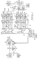
- amplifier 10 of the present invention is illustrated as a modulator for output stage 12 of a high power amplitude modulated radio frequency transmitter including tetrode 14.
- Tetrode 14 includes anode 16 to which the output voltage of amplifier 10 is applied.
- Anode 16 feeds antenna 18 via antenna coupling network 20.
- Tetrode 12 also includes screen grid 22, supplied with DC bias voltage by screen supply 24.
- Tetrode 12 also includes grounded cathode 26 and control grid 28, connected to carrier supply 30 and bias source 32 which cause the tetrode to be class C driven.
- Variable DC voltage that is a high voltage replica of the input of amplifier 10 (derived from audio AC modulation source 38, typically a music or voice source) is applied to plate 16 by the output of low pass filter 32, including series inductor 34 and shunt capacitor 36. Filter 32 is supplied with a varying high voltage DC step-wise waveform that is an approximate replica of AC source 38.
- the varying voltage applied to lowpass filter 32 is derived from M identical series-connected electronic switched stages 40.1, 40.2, 40.3,...40.(M-2), 40.(M-1), 40.M, selectively activated to only one of two bi-level states as a function of the amplitude of source 38; M is a relatively large number, e.g. somewhat in excess of 48.
- M is a relatively large number, e.g. somewhat in excess of 48.
- Like components associated with the different identical stages bear the same reference numerals to the left of a decimal point, while components of the same stage have the same reference numeral, equal to the stage number, to the right of the decimal point. When the stages and elements associated therewith are discussed in general only the reference numerals to the left of the decimal point are used.
- stages 40 are sourced to a constant DC power supply voltage, while in the second state, the stages are unsourced.
- Each of stages 40 when sourced, typically supplies a voltage of about 750 volts to output terminals 42 and 44 thereof; in the unsourced state, each of stages 40 supplies virtually zero volts to the output terminals thereof.
- the voltage sum derived from the series-stacked stages is approximately 36 kilovolts and when all of the stages are unsourced, the voltage sum derived from stages 40 is approximately zero volts.
- the voltage supplied to lowpass filter 32 is capable of varying between approximately zero volts and approximately 36 kilovolts.
- the input voltage to filter 32 is 18 kilovolts; the maximum positive and negative voltages of source 38 (typically 2.4 and -2.4 volts respectively) result in voltages of 36 kilovolts and 0 volts being applied to the filter.
- Converter 44 includes two delta connected three-phase primary windings 48 and 50 driven in parallel by the output of three-phase source 46.
- Primary winding 48 is coupled by magnetic core 51 to wye connected secondary windings 52.2...52.(M-2), 52.(M) which in turn drive three-phase rectifiers 54.2...54.(M-2), 54.(M) for respectively supplying DC power to stages 40.2...40.(M-2) and 40.(M).
- Primary winding 50 is coupled by magnetic core 56 to wye connected secondary windings 52.1, 52.3...52.(M-1), in turn connected to drive three-phase rectifiers 54.1, 54.3...54.(M-1), for respectively supplying DC power to stages 40.1, 40.3 and 40.(M-1).
- primary winding 48 supplies power to even-numbered stages 40.2...40.(M-2), 40.(M) [where M is an even integer] while primary winding 50 supplies power to odd-numbered stages 40.1, 40.3...40.(M-1). Because stages 40 are driven to the sourced and unsourced states such that consecutively numbered stages are sourced and unsourced, loading of primary windings 48 and 50 is approximately the same.
- secondary windings 52.1, 52.3...52.(M-1), as well as the rectifiers and stages associated therewith, are located in physical proximity with each other and spaced from secondary windings 52.2...52.(M-2) and 52.(M) as well as the stages and rectifiers associated therewith. Controls for the even-numbered stages are provided by coupling appropriate signals to the even and odd-numbered stages by low-level signal couplers.
- the secondary windings 52.1, 52.2...52.(M) are as illustrated for convenience in describing and illustrating the parts.
- Low-power control circuit 60 Control of which and how many of stages 40 are in the sourced and unsourced state is provided by low-power control circuit 60, including output leads 62.1, 62.2...62.(M), respectively supplying low-level signals to stages 40.1, 40.2...40.(M).
- Low-power control circuit 60 supplies bi-level signals to leads 62.
- the bi-level signals are pulsewidth modulated and have a predetermined frequency, i.e., predetermined period.
- circuit 62 supplies to each of leads 62 a bi-level signal having a duty cycle of 50 percent.
- the bi-level signals applied to leads 62 are phased displaced from each other so that the signals on adjacent leads are phase displaced by 1/48th of a cycle, i.e., 7.5°.
- control circuit 60 While such a constant voltage is derived from source 38, there are constant transitions in the bi-level signals supplied to each of leads 62.
- binary 1 levels are supplied by circuit 60 to leads 62.1-62.( M / 2), while binary 0 levels are supplied to leads 62.( M / 2+1)-62.(M).
- Control circuit 60 is arranged so that it effectively includes, for each of stages 40, a different variable threshold.
- the threshold for each stage is varied continuously by the output of triangular wave voltage controlled oscillator (VCO) 64 having a constant peak-to-peak amplitude that is a small percentage of the maximum voltage of AC modulation source 38.
- VCO triangular wave voltage controlled oscillator
- the maximum peak to peak output voltage of triangular wave voltage controlled oscillator 64 is 0.1 volts.
- Voltage controlled oscillator 64 is preferably of the type disclosed in commonly-assigned U.S. Patent 4,896,372.
- Voltage controlled oscillator 64 derives a variable frequency output having a nominal predetermined value, considerably in excess of the maximum frequency of source 38.
- the nominal frequency of oscillator 64 is 70 kHz.
- voltage controlled oscillator 64 is basically a frequency modulator, the oscillator produces sidebands that are positively and negatively displaced relative to the oscillator nominal frequency. Since input terminal 66 of triangular wave voltage controlled oscillator 64 is responsive, inter alia , to the output of AC modulation source 38, the negative sidebands can cause the output of the VCO to extend into the spectrum of source 38.
- variable frequency triangular wave output of voltage controlled oscillator 64 is linearly combined, in summing network 68, with the output of AC modulation source 38.
- the output of network 68 is an analog voltage having an amplitude equal to the amplitude of the output of modulation source 38 plus the amplitude of the output of triangular wave voltage controlled oscillator 64.
- the analog output of network 68 is applied to low-power control circuit 60 to control the bi-level control signals for stages 40.
- the frequency of oscillator 64 is controlled by the amplitude and frequency of source 38 because greater fidelity of the replica derived from low-pass filter 32 to the signal of source 38 is obtained by such control.
- controlling the frequency of oscillator 64 in this manner in response to the output of modulator 38 causes the oscillator to produce, in certain instances, components which affect the switching of stages 40. This somewhat spurious switching of stages 40 is noticeable as a noise component in the signal supplied by low-pass filter 32 to plate 16.
- the spectrum of the noise is spread so that there is no predominant frequency component introduced as a result of oscillator 64 being responsive to the output of modulation source 38.
- the spectrum derived from oscillator 64 is spread in this manner by supplying noise source 70 to input terminal 66 of voltage-controlled triangular wave oscillator 64.
- the output of noise source 70 is linearly combined with the output of AC modulation source 38 in summing network 72, having an output which is supplied to input terminal 66 of the oscillator.
- the spectrum of the noise derived from source 70 is limited so that the noise source does not cause excessive modulation of oscillator 64 and possibly introduce additional noise in the output of the amplifier.
- noise source 70 comprises a high gain DC operational amplifier having input terminals connected to a resistor and output terminals connected to a low pass filter having a cutoff frequency of 10 kHz. It is to be understood, however, that other appropriate noise sources can be employed.
- each stage derives on lead 74 a signal having binary one and zero values respectively indicative of the particular stage being in operative and failed states.
- the signals on leads 74 are coupled to circuit 60 to control the outputs thereof while source 38 is being applied to amplifier 10 so that the sum of the outputs of stages 40 applied to filter 32 is a step wise replica of source 38.
- Amplifier 10 supplies filter 32 with a voltage having a value that is a predetermined function of the amplitude of source 38 even if there is a failure of one or a few of stages 40 while source 38 is being supplied to the amplifier. Details of the circuitry for providing this result are described infra .
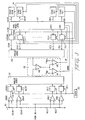
- FIG. 2 A circuit diagram for one embodiment of each of stages 40 is illustrated in Fig. 2.
- Each of stages 40 is provided with DC power by three-phase rectifier 54 for converting the three-phase AC voltage at secondary winding 52 into a DC voltage.
- Rectifier 54 drives shunt capacitor 102 across which is developed a 750 volt DC power supply voltage. The voltage across capacitor 102 is selectively switched to output terminals 42 and 44 through the series connected emitter collector paths of isolated gate bipolar transistors 103 and 203 although other similar devices can be used.
- Transistors 103 and 203 have bipolar emitter-collector characteristics and high impedance gate, i.e., control electrode, characteristics similar to those of a metal oxide semiconductor field effect transistor.
- Transistors 103 and 203 include collector and emitter electrodes such that the collector of transistor 103 is connected to one electrode of capacitor 102 and the emitter of transistor 203 is connected to the cathode of diode 104; the emitter of transistor 103 is connected directly to the collector of transistor 203.
- the anode of diode 104 is connected to the remaining electrode of capacitor 102.
- Diode 104 is connected across output terminals 42 and 44.
- Bias control between the gate and emitter of transistors 103 and 203 is provided by circuit 105 that switches the emitter collector paths of transistors 103 and 203 between a saturated and non-conducting state.
- transistor 203 is biased to the saturated state and transistor 103 is controlled by the output of circuit 60 on lead 62. (Normal operation is now assumed.)
- the saturated state of transistor 103 the DC voltage across capacitor 102 is coupled to terminals 42 and 44, while causing diode 104 to be back biased.
- transistor 103 is not conducting, the voltage between terminals 42 and 44 drops quickly to zero by virtue of the relatively low impedance path provided through the anode and cathode of diode 104. Thereby, the impedance between terminals 42 and 44 is maintained at a first predetermined constant value while transistor 103 is in a conducting state, and is maintained at a second, much lower predetermined value while the transistor is not conducting.
- Drive control and logic circuit 105 is controlled by an opto-electronic link including photodiode 106, connected to input terminals of circuit 105 via current limiting resistor 107.
- Diode 106 is optically coupled (e.g. by a fiber optic link) to light emitting diode 108, connected via resistor 111 to be responsive to a signal supplied by low power control circuit 60 to the lead 62 associated with the particular stage including transistor 103.
- the signal on lead 62 has binary one and zero values to command turn on and turn off of the switch comprising transistor 103.
- diode 108 In response to the signal on lead 62 being a binary one level, diode 108 is activated to illuminate photodiode 106. In contrast, diode 108 derives no optical signal in response to a binary zero level on lead 62. In response to diode 106 being illuminated, circuit 105 supplies a positive forward bias to the gate of transistor 103 via lead 111 to cause transistor 103 to be in the saturated state. When no optical energy is incident on diode 106, circuit 105 back biases the gate of transistor 103 so transistor 103 does not conduct.
- the emitter collector path of transistor 203 connected in series with the emitter collector path of transistor 103, is normally forward biased by an output of circuit 105 on lead 211 so that operation of transistor 103 controls the state of the particular stage. However, if the particular output stage 40 is not operating properly the transistor 203 of that stage is biased to cut off. Proper operation of the stage is detected by drive control and logic circuit 105 comparing the bi-level signal derived from photodiode 106 with the output voltage derived from the stage, as developed across diode 104. If the signal derived from photodiode 106 and the stage output voltage do not correlate, transistor 203 is cut off to cause the particular stage to become inoperative and its operation to be automatically replaced by another output stage 40. The inoperativeness of one or a few output stages does not adversely affect operation of the amplifier.
- a feedback arrangement (described infra ) in control circuit 60 automatically causes the correct number of stages 40 to be sourced and unsourced.
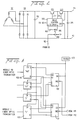
- Figs. 3 and 4 One preferred embodiment of the circuitry included in low-power control circuit 60 is illustrated in Figs. 3 and 4.
- the output of summing circuit 68 is applied in parallel to negative input terminals of comparators 209, one of which is provided for each of stages 40 that can be sourced. If, e.g. 48 stages 40 can be sourced, 48 comparators 209 are provided. In the typical situation one or a few spare output stages 40 are included so that if 48 output stages can be sourced for a maximum signal of source 38, 52 output stages are included.
- 48 of comparators 209 are provided to enable 48 of stages 40.1-40.M (where M>48) to be sourced.
- Positive input terminals of comparators 209.1-209.48 are responsive to different DC voltages at taps of voltage divider 161, energized by the positive DC voltage at terminal 162.
- Each of resistors 163.2, 163.3...163.47, 163.48, respectively connected to the positive input terminals of comparators 209.2, 209.3...209.47, 209.48 has an identical value so that in one preferred embodiment wherein the maximum peak to peak voltage of source 38 is 4.8 volts and the maximum peak to peak voltage derived by VCO 64 is 0.1 volts, the voltage between adjacent taps of the voltage divider is 0.1 volts.
- the voltages at the taps of voltage divider 161 establish median threshold voltages for the comparators 209 connected to the taps.
- the threshold is constantly linearly varied about the median value therefor by the triangular wave output of source 68.
- the comparator In response to the amplitude of the voltage at the negative input terminal of a particular comparator 209 exceeding the voltage at the positive input terminal of that comparator, the comparator derives a binary one output. Conversely, in response to the amplitude of the voltage at the positive input terminal of a particular comparator 209 exceeding the voltage at the negative input terminal of that comparator, the comparator derives a binary zero output.
- comparators 209.1, 209.2...209.(N) derive binary one levels
- comparators 209.(N+2), 209.(N+3)...209.48 derive binary zero levels
- comparator 209.(N+1) derives a bi-level pulse width modulated wave having a duty cycle k, as averaged over one cycle of source 38.
- stages 40.7-40.30 may be sourced; during a subsequent instant stages 40.8-40.31 may be sourced.
- the number of comparators 209.1-209.48 deriving binary one levels is indicated by supplying the binary one output levels of these comparators to analog adding network 121.
- the output voltage of analog adding network 121 is a DC voltage having, at any one time, one of 48 possible values.
- Each of the possible output values of analog adder 121 represents the number of comparators 209.1-209.48 which is deriving a binary one level.
- comparators 209.2-209.48 are sampled many times during each cycle of triangle wave source 68 by respectively supplying the outputs of comparators 209.1-209.48 to sample and hold, i.e., latch networks 122.1-122.48, also responsive to clock source 123, having a frequency of several megaHertz.
- the latched outputs of latches 122.1-122.48 are applied to analog summing circuit 121. As variations in modulation source 38 and triangular wave source 68 occur, the output level of circuit 121 changes accordingly.
- the output signal of adder 121 is compared with a signal indicative of the number of stages 40 in a sourced state, as derived from analog adder 125.
- Adder 125 is responsive to latch networks 133.1-133.48 respectively responsive to the different binary states of ring modulator 127 and clock 123.
- Analog adder 125 derives an output having one of 48 different levels, each representing the sourced and non-sourced states of stages 40.
- the output signals of adders 121 and 125 are supplied to analog comparator 126 which selectively derives one of two positive going, i.e., binary zero to one, transitions as a function of the output signals of adders 121 and 125.
- Comparator 126 includes difference amplifier 140 as well as comparators 141 and 142; amplifier 140 has plus and minus inputs respectively responsive to the voltages derived by adders 121 and 125.
- the output of amplifier 140 is applied in parallel to negative and positive inputs of comparators 141 and 142, having positive and negative inputs respectively responsive to negative and positive DC reference voltages, -Vref and +Vref, where Vref is typically 50 millivolts.
- comparator 141 derives a binary one level; in response to the voltage at the positive input of amplifier 142 exceeding +Vref, comparator 142 derives a binary one output. If the output of difference amplifier 140 is in a dead band from -Vref to +Vref, the output of comparators 141 or 142 are at the binary zero level and no changes occur in ring modulator 127.
- the transitions at the outputs of comparator 126 control which of output stages 40 are in the sourced and non-sourced states.
- the outputs of comparator 126 are supplied to two separate input terminals of ring modulator 127, also responsive to clock source 123.
- Ring modulator 127 includes an output lead for each of output stages 40.
- the number of output stages 40 in a sourced state is generally equal to the number of comparators 209.1-209.48 deriving binary one levels. However, there is no other correlation between which of stages 40 are sourced and which of comparators 109.1-109.48 are deriving binary one levels.
- Ring modulator 127 includes two sets of output leads 128 and 129 (one for each of output stages 40) respectively driven in parallel by binary signals representing which of stages 40 are sourced and non-sourced.
- the signals on output leads 128 are supplied as control inputs to stages 40. These controls include fiber optic links, as described supra .
- the signals on output leads 128 are supplied as inputs to latches 133 (one for each of output stages 40), thence to analog adder 125.
- ring modulator 127 Details of a preferred embodiment of ring modulator 127 are illustrated in Fig. 4 as including two M stage recirculating shift registers 131 and 132 and M output latches 133, each configured as a J-K flip-flop.
- Each of shift registers 131 and 132 includes an increment (INC) input terminal responsive to a separate output of comparator network 126 and a clock input terminal responsive to clock source 123.
- Shift registers 131 and 132 are driven only in a forward direction, so that in response to transitions supplied to the increment inputs thereof, the shift register stage in a binary one state is advanced by a count of one. Only one stage of shift registers 131 and 132 is in a binary one state at a particular time.
- stage M When a binary one state is in the final stage, i.e., stage M, of each of shift registers 131 and 132 the binary one state of the shift register advances to stage one in response to the next occurrence of a positive going transition at the increment input terminal of the shift register.
- the state of shift registers 131 and 132 is advanced during the positive going transition of clock 123 immediately following a positive going transition at the increment input of the shift register.
- Shift register 131 is incremented in response to binary zero to one transitions in the output of comparator 141, while shift register 132 is incremented in response to binary zero to one transitions in the output of comparator 142.
- the outputs of comparators 142 and 141 are respectively connected to the increment inputs of shift registers 132 and 131.
- Each of latches 133 includes a set (S) and a reset (R) input, as well as a clock input.
- the clock inputs of latches 133 are driven in parallel by the output of clock source 123.
- the set inputs of latches 133.1-133.(M) are respectively connected to output leads of each of stages 1-M of shift register 132.
- the reset inputs of latches 133.1-133.M are respectively connected to output leads of each of stages 1-M of shift register 131.
- the output terminals of latches 133.1-133.(M) supply binary one levels to output leads 127.1-127.(M) and 128.1-128.(M) when the latches are set, i.e., in a binary one state.
- Each of latches 133 is of a type such that the latches, i.e., flip-flops, are in a binary zero state in response to a binary zero state being supplied to the reset inputs thereof during the previous clock pulse input thereof.
- Latches 133 are in a binary one state in response to a binary one state being applied to the set inputs thereof during the previous clock pulse input thereof. If a binary one is applied to both the reset and set inputs of a particular latch 133 during a particular clock period, the output state of the particular flip-flop toggles to the opposite binary state, i.e., changes from one to zero or zero to one. Changes in the states of latches 133 occur only during a positive going transition of clock 123 following a binary zero to one transition at the set or reset input of the particular flip-flop.
- Conventional reset circuitry causes shift registers 131 and 132 to be activated so that stage one thereof is initially set to a binary one state, while each of latches 133 is initially in the reset condition.
- the stages of shift registers 131 and 132 having binary one values therein generally indicate the limits of output stages 40 which are respectively in the reset and set stages; these stages of shift registers 131 and 132 are respectively represented by N(r) and N(s). If N(s) is greater than N(r), output stages 40.N(r+1) through 40.N(s) are sourced while output stages 40.1 through 40.N(r) and 40.N(s+1) through 40.M are non-sourced. If N(r) is greater than N(s), output stages 40.N(r) through 40.N(s-1) are non-sourced while output stages 40.1 through 40.N(r-1) and 40.N(s) through 40.48 are sourced. If N(r) equals N(s), either all or none of output stages 40.1 through 40.(M) are sourced.
- the number of output stages 40 which should be in a sourced state, indicated by the output of adder 121, is compared in comparator 126 with the number of output stages 40 in a sourced state, as indicated by the output of adder 125.
- the count in shift register 132 is incremented by a count of one during that cycle time; conversely shift register 131 is incremented by a count of one in response to the output of adder 125 exceeding that of adder 121 during a cycle time of clock 123.
- the output voltages of stages 40 have transitions between zero and 750 volts in response to transitions of triangular wave source 64 relative to the amplitude of source 38. The time between these transitions is controlled by the amplitude of source 38. However, different stages 40 are activated into the sourced state at different times in response to the variations of triangular wave source 64. Thereby, the substantial power which is dissipated in the different output stages 40 is shared by these stages.
- the voltage of AC modulation source 38 remains constant at a voltage less than the voltage associated with the threshold of one stage, only one of output stages 40 is activated into the sourced state at a time.
- the sourced duration of a particular stage is determined by the amplitude of source 38. All of stages 40 are sequentially activated to the sourced state, at a frequency determined by the frequency of source 71.
- the switching frequency of a particular output stage 34 is basically equal to the frequency of source 64 divided by the number of output stages; typically the switching frequency is about 2 kHz, so that switching losses in each output stage are relatively low.
- the voltage of source 38 varies, the number of output stages 40 in a sourced state varies accordingly, as is the conducting interval of one of the stages.
- control of output stages 40 is determined by an indication of the number of output stages to be sourced, instead of which specific stages are to be sourced, the number of series connected output stages 40 can be, and preferably is, greater than the number of stages required to derive the amplifier maximum output voltage. Thereby, if an output stage 40 fails, there is no disruption in proper operation of the amplifier and the sum of the voltages supplied by the output stages to filter 32 remains a step wise replica of the amplitude of analog source 38.
- each of drive control and logic circuits 105 includes an opto-electronic link, similar to the link including diodes 106 and 108.
- a signal is derived on lead 74 by circuit 105 (Fig. 2) of the output stage. The signal on lead 74 is supplied to the latch 129 corresponding with the failed output stage to prevent derivation of a positive, binary one output of that latch.
- stages 40 in excess of the number of comparators 209) enable a maximum output voltage to be obtained in the event of a failure of one or a few output stages. Hence, in the event of a failure of one or a few output stages, correct operation continues because comparator 126 derives a signal indicating that a further output stage is to be sourced.
Description
- The present invention relates generally to amplifiers and more particularly to an amplifier having at least several stages activated only to bi-level outputs which are summed together, which amplifier includes provisions for substantial noise reduction.
- U.S. Patent No. 5,099,203, issued March 24, 1992, discloses an amplifier responsive to a signal source comprising at least several stages activated only to one of two bi-level states (sourced and unsourced) controlled in response to the value of a signal source exceeding a different threshold for each stage. The thresholds and source are arranged so that the stages change between the bi-level states as the value of the source changes relative to the thresholds of the different stages. Bi-level outputs associated with the bi-level states of the plural stages are summed together. The values of the thresholds are continuously varied by a small amount relative to a predetermined maximum value for the source. In the preferred embodiment, the threshold values are varied by applying a wave having a continuously varying amplitude in parallel to the various stages. Preferably, the continuously varying wave is derived from a variable frequency voltage controlled oscillator and is a triangular wave having a frequency determined by the amplitude and frequency of the signal source. As the amplitude and frequency of the signal source increase the triangular wave frequency increases from a nominal value thereof. The amplifier disclosed in the co-pending application is, in a preferred use, responsive to an audio signal source, e.g. speech or music, and is part of an amplifier for controlling plate modulation of a high-power amplitude modulated radio frequency transmitter. The output wave derived from the amplifier is a high-voltage replica of the input signal supplied to the amplifier.
- In the preferred embodiment of the prior art amplifier, 48 output stages are employed. The output stages are powered by an AC to DC converter arrangement driven by a three-phase source. The AC to DC converter arrangement includes two primary windings and a secondary winding for each output stage. Each secondary winding is connected to a separate rectifier for supplying DC energizing voltage to the stage associated with it. One primary winding is coupled via a magnetic core to the secondary windings powering output stages 1-24, while the second primary winding is coupled via a second core to the secondary windings which drive output stages 25-48. The output stages are energized by control circuitry for them so that consecutively numbered stages are activated to a first of the bi-level states and the remaining output stages are activated to the other bi-level state. In the preferred embodiment of the prior art, there is a continual change at a predetermined frequency of which output stages are sourced. The change occurs even if there is no change in the amplitude of the input signal over a certain time. Such continuous changing obviates the tendency for certain stages to be virtually continuously dissipating power while other stages virtually never dissipate power.
- The amplifier disclosed in the above-mentioned application functions admirably for many situations. For other situations, the amplifier, through actual testing, has been found to produce excessive noise components. I have determined that two sources of the excessive noise components are (1) unequal loading of the two primary windings coupled to the secondary windings which drive the output stages and (2) excessively high amplitude components associated with changing the thresholds in switching the stages between the bi-level states.
- The first noise components are at a frequency determined by the number of output stages and the frequency at which the stages are switched. To understand how the first noise components are derived, consider the situation wherein the input signal is constant, at zero AC amplitude, resulting in one-half of the output stages being in the sourced state and the remaining output stages being unsourced. At one instant of time, stages 1-24 are sourced, while stages 25-48 are unsourced. At a second time instant, a few milliseconds after the first time instant, stages 1-12 and 37-48 are unsourced simultaneously with stages 13-36 being sourced. At a third time instant, displaced a few milliseconds from the second time instant, stages 1-24 are unsourced and stages 25-48 are sourced.
- During the first mentioned time instant, the first primary winding is fully loaded and the second primary winding is completely unloaded. Thereby, the voltage supplied by the first transformer to stages 1-24 is a relatively low voltage. The sum of the output voltages derived from stages 1-24 is thereby somewhat lower than expected. At the second time instant, the voltages of the two primary windings are approximately halfway between the minimum voltage, as occurs when the primary windings are fully loaded, and the maximum transformer primary windings, which occurs when the primary windings are completely unloaded. Thereby, the voltages supplied to stages 13-36 are greater than during the first time instant and the sum of the output voltages derived from these 24 stages during the second instant is somewhat greater than the sum of the output voltages derived from stages 1-24 during the firstmentioned instant. During the third instant, the second primary winding is fully loaded, causing the sum of the output voltages of stages 25-48 to be virtually the same as during the first mentioned instant. Hence, the resultant sum of the output voltages of all 48 stages varies at a frequency determined by the number of stages and the switching frequency of the stages, even though there is no change in the amplitude of the input signal driving the amplifier.
- The second source of the noise components, excessively high amplitude components associated with changing the thresholds of the states in switching the stages between the bi-level states, occurs as a result of the tendency of the variable frequency voltage controlled oscillator to produce sidebands in the frequency band of the input signal being amplified. The voltage controlled oscillator, preferably of the type disclosed in commonly assigned United States Patent 4,896,372, has a nominal frequency, such as 70 kHz, considerably above the 5 or 10 kHz bandwidth of the input audio signal source. In response to increases in the amplitude and frequency of the input source, the output frequency of the voltage controlled oscillator increases relative to the nominal 70 kHz value thereof. In addition to the increased frequency of the voltage controlled oscillator output, I have found that the oscillator derives sidebands having frequency components that can overlap into the spectrum of the input signal. Due to the nature in which the sidebands are derived, as governed by Bessel function relationships, the amplitude of the overlapping sidebands can be relatively high. Since the voltage controlled oscillator output determines the threshold level of the output stages, the relatively high amplitude overlapping sidebands derived from the voltage controlled oscillator introduce noise in the output of the amplifier.
- EP-A-0267391 discloses an amplifier responsive to a signal source comprising at least several power output stages activated only to one of two bi-level states controlled in response to the value of the source, bi-level voltage outputs associated with the bi-level states of the plural stages being summed together, power supply means including an AC to DC converter for said stages, said converter including plural primary windings. The present invention improves on this arrangement as set out in the characterising clause of
claim 1. - There are three divisional applications divided from parent application 92308665.6 (EP-A-0549101) and all relate to similar subject matter.
- An example of the invention will now be described with reference to the accompanying drawings in which:
- Fig. 1 is a partial schematic, partial block diagram of a transmitter including a preferred embodiment of an amplifier in accordance with a preferred embodiment of the invention.
- Fig. 2 is a schematic diagram of a stage that can be employed in the amplifier of Fig. 1;
- Fig. 3 is a partial block, partial schematic diagram of a low power amplifier employed in Fig. 1; and
- Fig. 4 is a block diagram of digital circuitry employed in the low power amplifier of Fig. 3.
-
- Reference is now made to Fig. 1 of the drawing wherein
amplifier 10 of the present invention is illustrated as a modulator foroutput stage 12 of a high power amplitude modulated radio frequencytransmitter including tetrode 14.Tetrode 14 includesanode 16 to which the output voltage ofamplifier 10 is applied. Anode 16 feeds antenna 18 via antenna coupling network 20.Tetrode 12 also includes screen grid 22, supplied with DC bias voltage byscreen supply 24. Tetrode 12 also includesgrounded cathode 26 andcontrol grid 28, connected tocarrier supply 30 andbias source 32 which cause the tetrode to be class C driven. - Variable DC voltage that is a high voltage replica of the input of amplifier 10 (derived from audio
AC modulation source 38, typically a music or voice source) is applied toplate 16 by the output oflow pass filter 32, includingseries inductor 34 andshunt capacitor 36.Filter 32 is supplied with a varying high voltage DC step-wise waveform that is an approximate replica ofAC source 38. - The varying voltage applied to
lowpass filter 32 is derived from M identical series-connected electronic switched stages 40.1, 40.2, 40.3,...40.(M-2), 40.(M-1), 40.M, selectively activated to only one of two bi-level states as a function of the amplitude ofsource 38; M is a relatively large number, e.g. somewhat in excess of 48. Like components associated with the different identical stages bear the same reference numerals to the left of a decimal point, while components of the same stage have the same reference numeral, equal to the stage number, to the right of the decimal point. When the stages and elements associated therewith are discussed in general only the reference numerals to the left of the decimal point are used. - In one state, stages 40 are sourced to a constant DC power supply voltage, while in the second state, the stages are unsourced. Each of stages 40, when sourced, typically supplies a voltage of about 750 volts to
output terminals lowpass filter 32 is capable of varying between approximately zero volts and approximately 36 kilovolts. When the voltage ofsource 38 is zero, the input voltage to filter 32 is 18 kilovolts; the maximum positive and negative voltages of source 38 (typically 2.4 and -2.4 volts respectively) result in voltages of 36 kilovolts and 0 volts being applied to the filter. - Power is supplied to stages 40 by AC to
DC converter network 44 responsive to three-phase source 46. Converter 44 includes two delta connected three-phaseprimary windings phase source 46. Primary winding 48 is coupled bymagnetic core 51 to wye connected secondary windings 52.2...52.(M-2), 52.(M) which in turn drive three-phase rectifiers 54.2...54.(M-2), 54.(M) for respectively supplying DC power to stages 40.2...40.(M-2) and 40.(M). Primary winding 50 is coupled bymagnetic core 56 to wye connected secondary windings 52.1, 52.3...52.(M-1), in turn connected to drive three-phase rectifiers 54.1, 54.3...54.(M-1), for respectively supplying DC power to stages 40.1, 40.3 and 40.(M-1). Thus, primary winding 48 supplies power to even-numbered stages 40.2...40.(M-2), 40.(M) [where M is an even integer] while primary winding 50 supplies power to odd-numbered stages 40.1, 40.3...40.(M-1). Because stages 40 are driven to the sourced and unsourced states such that consecutively numbered stages are sourced and unsourced, loading ofprimary windings primary windings - In the preferred physical arrangement, secondary windings 52.1, 52.3...52.(M-1), as well as the rectifiers and stages associated therewith, are located in physical proximity with each other and spaced from secondary windings 52.2...52.(M-2) and 52.(M) as well as the stages and rectifiers associated therewith. Controls for the even-numbered stages are provided by coupling appropriate signals to the even and odd-numbered stages by low-level signal couplers. The secondary windings 52.1, 52.2...52.(M) are as illustrated for convenience in describing and illustrating the parts.
- Control of which and how many of stages 40 are in the sourced and unsourced state is provided by low-
power control circuit 60, including output leads 62.1, 62.2...62.(M), respectively supplying low-level signals to stages 40.1, 40.2...40.(M). Low-power control circuit 60 supplies bi-level signals to leads 62. The bi-level signals are pulsewidth modulated and have a predetermined frequency, i.e., predetermined period. For a constant, zero amplitude signal derived fromAC modulation source 38, as associated with a period of silence,circuit 62 supplies to each of leads 62 a bi-level signal having a duty cycle of 50 percent. The bi-level signals applied toleads 62 are phased displaced from each other so that the signals on adjacent leads are phase displaced by 1/48th of a cycle, i.e., 7.5°. During each cycle of operation ofcontrol circuit 60 while such a constant voltage is derived fromsource 38, there are constant transitions in the bi-level signals supplied to each of leads 62. Hence, during one instant, binary 1 levels are supplied bycircuit 60 to leads 62.1-62.( M / 2), while binary 0 levels are supplied to leads 62.( M / 2+1)-62.(M). One-half cycle of the operation ofcontrol circuit 60 after the previously mentioned instant, the situation is reversed so that 0 binary levels are supplied to leads 62.1-62.( M / 2) whilebinary 1 levels are supplied to leads 62. leads 62.( M / 2+1)-62.(M). The binary levels onleads 62 control which of switches or stages 40 are sourced and unsourced. Hence, there are repeated transitions in the stages 40 which are sourced and unsourced, so that the tendency of power to be dissipated in certain of the stages, to the exclusion of the other stages, is obviated. -
Control circuit 60 is arranged so that it effectively includes, for each of stages 40, a different variable threshold. The threshold for each stage is varied continuously by the output of triangular wave voltage controlled oscillator (VCO) 64 having a constant peak-to-peak amplitude that is a small percentage of the maximum voltage ofAC modulation source 38. In the preferred embodiment wherein the maximum peak to peak voltage ofsource 38 is 4.8 volts, the maximum peak to peak output voltage of triangular wave voltage controlledoscillator 64 is 0.1 volts. Voltage controlledoscillator 64 is preferably of the type disclosed in commonly-assigned U.S. Patent 4,896,372. - Voltage controlled
oscillator 64 derives a variable frequency output having a nominal predetermined value, considerably in excess of the maximum frequency ofsource 38. In a preferred embodiment, the nominal frequency ofoscillator 64 is 70 kHz. As the amplitude and frequency of the control voltage supplied tooscillator 64 at input terminal 66 thereof increase from zero values therefor, the frequency of the oscillator increases relative to the nominal value thereof. Because voltage controlledoscillator 64 is basically a frequency modulator, the oscillator produces sidebands that are positively and negatively displaced relative to the oscillator nominal frequency. Since input terminal 66 of triangular wave voltage controlledoscillator 64 is responsive, inter alia, to the output ofAC modulation source 38, the negative sidebands can cause the output of the VCO to extend into the spectrum ofsource 38. - To control the variable thresholds for switches 40.1-40.48, the variable frequency triangular wave output of voltage controlled
oscillator 64 is linearly combined, in summingnetwork 68, with the output ofAC modulation source 38. At any instant of time, the output ofnetwork 68 is an analog voltage having an amplitude equal to the amplitude of the output ofmodulation source 38 plus the amplitude of the output of triangular wave voltage controlledoscillator 64. The analog output ofnetwork 68 is applied to low-power control circuit 60 to control the bi-level control signals for stages 40. - The frequency of
oscillator 64 is controlled by the amplitude and frequency ofsource 38 because greater fidelity of the replica derived from low-pass filter 32 to the signal ofsource 38 is obtained by such control. However, controlling the frequency ofoscillator 64 in this manner in response to the output ofmodulator 38 causes the oscillator to produce, in certain instances, components which affect the switching of stages 40. This somewhat spurious switching of stages 40 is noticeable as a noise component in the signal supplied by low-pass filter 32 toplate 16. - In accordance with one aspect of the present invention, the spectrum of the noise is spread so that there is no predominant frequency component introduced as a result of
oscillator 64 being responsive to the output ofmodulation source 38. The spectrum derived fromoscillator 64 is spread in this manner by supplyingnoise source 70 to input terminal 66 of voltage-controlledtriangular wave oscillator 64. The output ofnoise source 70 is linearly combined with the output ofAC modulation source 38 in summingnetwork 72, having an output which is supplied to input terminal 66 of the oscillator. The spectrum of the noise derived fromsource 70 is limited so that the noise source does not cause excessive modulation ofoscillator 64 and possibly introduce additional noise in the output of the amplifier. - In one preferred embodiment,
noise source 70 comprises a high gain DC operational amplifier having input terminals connected to a resistor and output terminals connected to a low pass filter having a cutoff frequency of 10 kHz. It is to be understood, however, that other appropriate noise sources can be employed. - To prevent distortion in the event of a failure of one or a few of stages 40, each stage derives on lead 74 a signal having binary one and zero values respectively indicative of the particular stage being in operative and failed states. The signals on
leads 74 are coupled tocircuit 60 to control the outputs thereof whilesource 38 is being applied toamplifier 10 so that the sum of the outputs of stages 40 applied to filter 32 is a step wise replica ofsource 38.Amplifier 10 supplies filter 32 with a voltage having a value that is a predetermined function of the amplitude ofsource 38 even if there is a failure of one or a few of stages 40 whilesource 38 is being supplied to the amplifier. Details of the circuitry for providing this result are described infra. - A circuit diagram for one embodiment of each of stages 40 is illustrated in Fig. 2. Each of stages 40 is provided with DC power by three-
phase rectifier 54 for converting the three-phase AC voltage at secondary winding 52 into a DC voltage.Rectifier 54 drives shuntcapacitor 102 across which is developed a 750 volt DC power supply voltage. The voltage acrosscapacitor 102 is selectively switched tooutput terminals bipolar transistors Transistors Transistors transistor 103 is connected to one electrode ofcapacitor 102 and the emitter oftransistor 203 is connected to the cathode ofdiode 104; the emitter oftransistor 103 is connected directly to the collector oftransistor 203. The anode ofdiode 104 is connected to the remaining electrode ofcapacitor 102.Diode 104 is connected acrossoutput terminals - Bias control between the gate and emitter of
transistors circuit 105 that switches the emitter collector paths oftransistors transistor 203 is biased to the saturated state andtransistor 103 is controlled by the output ofcircuit 60 onlead 62. (Normal operation is now assumed.) In the saturated state oftransistor 103, the DC voltage acrosscapacitor 102 is coupled toterminals diode 104 to be back biased. Whentransistor 103 is not conducting, the voltage betweenterminals diode 104. Thereby, the impedance betweenterminals transistor 103 is in a conducting state, and is maintained at a second, much lower predetermined value while the transistor is not conducting. - Drive control and
logic circuit 105 is controlled by an opto-electroniclink including photodiode 106, connected to input terminals ofcircuit 105 via current limitingresistor 107.Diode 106 is optically coupled (e.g. by a fiber optic link) tolight emitting diode 108, connected via resistor 111 to be responsive to a signal supplied by lowpower control circuit 60 to thelead 62 associated with the particularstage including transistor 103. The signal onlead 62 has binary one and zero values to command turn on and turn off of theswitch comprising transistor 103. - In response to the signal on
lead 62 being a binary one level,diode 108 is activated to illuminatephotodiode 106. In contrast,diode 108 derives no optical signal in response to a binary zero level onlead 62. In response todiode 106 being illuminated,circuit 105 supplies a positive forward bias to the gate oftransistor 103 via lead 111 to causetransistor 103 to be in the saturated state. When no optical energy is incident ondiode 106,circuit 105 back biases the gate oftransistor 103 sotransistor 103 does not conduct. - The emitter collector path of
transistor 203, connected in series with the emitter collector path oftransistor 103, is normally forward biased by an output ofcircuit 105 on lead 211 so that operation oftransistor 103 controls the state of the particular stage. However, if the particular output stage 40 is not operating properly thetransistor 203 of that stage is biased to cut off. Proper operation of the stage is detected by drive control andlogic circuit 105 comparing the bi-level signal derived fromphotodiode 106 with the output voltage derived from the stage, as developed acrossdiode 104. If the signal derived fromphotodiode 106 and the stage output voltage do not correlate,transistor 203 is cut off to cause the particular stage to become inoperative and its operation to be automatically replaced by another output stage 40. The inoperativeness of one or a few output stages does not adversely affect operation of the amplifier. A feedback arrangement (described infra) incontrol circuit 60 automatically causes the correct number of stages 40 to be sourced and unsourced. - One preferred embodiment of the circuitry included in low-
power control circuit 60 is illustrated in Figs. 3 and 4. The output of summingcircuit 68 is applied in parallel to negative input terminals of comparators 209, one of which is provided for each of stages 40 that can be sourced. If, e.g. 48 stages 40 can be sourced, 48 comparators 209 are provided. In the typical situation one or a few spare output stages 40 are included so that if 48 output stages can be sourced for a maximum signal ofsource - Positive input terminals of comparators 209.1-209.48 are responsive to different DC voltages at taps of voltage divider 161, energized by the positive DC voltage at
terminal 162. Each of resistors 163.2, 163.3...163.47, 163.48, respectively connected to the positive input terminals of comparators 209.2, 209.3...209.47, 209.48, has an identical value so that in one preferred embodiment wherein the maximum peak to peak voltage ofsource 38 is 4.8 volts and the maximum peak to peak voltage derived byVCO 64 is 0.1 volts, the voltage between adjacent taps of the voltage divider is 0.1 volts. - The voltages at the taps of voltage divider 161 establish median threshold voltages for the comparators 209 connected to the taps. The threshold is constantly linearly varied about the median value therefor by the triangular wave output of
source 68. In response to the amplitude of the voltage at the negative input terminal of a particular comparator 209 exceeding the voltage at the positive input terminal of that comparator, the comparator derives a binary one output. Conversely, in response to the amplitude of the voltage at the positive input terminal of a particular comparator 209 exceeding the voltage at the negative input terminal of that comparator, the comparator derives a binary zero output. Thereby if the signal ofsource 38 has a value of N+k, comparators 209.1, 209.2...209.(N) derive binary one levels, comparators 209.(N+2), 209.(N+3)...209.48 derive binary zero levels and comparator 209.(N+1) derives a bi-level pulse width modulated wave having a duty cycle k, as averaged over one cycle ofsource 38. - To control which of output stages 40 are in the sourced and non-sourced states, a comparison is made of the number of comparators 209.1-209.48 in the binary one state with the number of output stages 40 in the sourced state. The arrangement is such that if, for example, the amplitude of
source 38 remains constant, the number of output stages 40 in the sourced state remains constant; however, which ones of output stages 40 are activated constantly changes, despite the fact that the amplitude ofsource 38 does not change. For example, if the voltage ofsource 38 is one-half of the voltage atterminal source 38 is one-half of the voltage atterminal 162, stages 40.7-40.30 may be sourced; during a subsequent instant stages 40.8-40.31 may be sourced. During both instants, the sum of the voltages derived by stages 40 is 24 x 750 = 18,000 volts. - To these ends, the number of comparators 209.1-209.48 deriving binary one levels is indicated by supplying the binary one output levels of these comparators to
analog adding network 121. The output voltage ofanalog adding network 121 is a DC voltage having, at any one time, one of 48 possible values. Each of the possible output values ofanalog adder 121 represents the number of comparators 209.1-209.48 which is deriving a binary one level. - The outputs of comparators 209.2-209.48 are sampled many times during each cycle of
triangle wave source 68 by respectively supplying the outputs of comparators 209.1-209.48 to sample and hold, i.e., latch networks 122.1-122.48, also responsive toclock source 123, having a frequency of several megaHertz. The latched outputs of latches 122.1-122.48 are applied toanalog summing circuit 121. As variations inmodulation source 38 andtriangular wave source 68 occur, the output level ofcircuit 121 changes accordingly. - The output signal of
adder 121 is compared with a signal indicative of the number of stages 40 in a sourced state, as derived fromanalog adder 125.Adder 125 is responsive to latch networks 133.1-133.48 respectively responsive to the different binary states ofring modulator 127 andclock 123.Analog adder 125 derives an output having one of 48 different levels, each representing the sourced and non-sourced states of stages 40. The output signals ofadders analog comparator 126 which selectively derives one of two positive going, i.e., binary zero to one, transitions as a function of the output signals ofadders -
Comparator 126 includesdifference amplifier 140 as well ascomparators amplifier 140 has plus and minus inputs respectively responsive to the voltages derived byadders amplifier 140 is applied in parallel to negative and positive inputs ofcomparators amplifier 140 applied to the negative input ofcomparator 141 having a larger negative voltage than -Vref,comparator 141 derives a binary one level; in response to the voltage at the positive input ofamplifier 142 exceeding +Vref,comparator 142 derives a binary one output. If the output ofdifference amplifier 140 is in a dead band from -Vref to +Vref, the output ofcomparators ring modulator 127. - The transitions at the outputs of
comparator 126 control which of output stages 40 are in the sourced and non-sourced states. To this end, the outputs ofcomparator 126 are supplied to two separate input terminals ofring modulator 127, also responsive toclock source 123.Ring modulator 127 includes an output lead for each of output stages 40. The number of output stages 40 in a sourced state is generally equal to the number of comparators 209.1-209.48 deriving binary one levels. However, there is no other correlation between which of stages 40 are sourced and which of comparators 109.1-109.48 are deriving binary one levels. -
Ring modulator 127 includes two sets of output leads 128 and 129 (one for each of output stages 40) respectively driven in parallel by binary signals representing which of stages 40 are sourced and non-sourced. The signals on output leads 128 are supplied as control inputs to stages 40. These controls include fiber optic links, as described supra. The signals on output leads 128 are supplied as inputs to latches 133 (one for each of output stages 40), thence toanalog adder 125. - Details of a preferred embodiment of
ring modulator 127 are illustrated in Fig. 4 as including two M stage recirculatingshift registers 131 and 132 and M output latches 133, each configured as a J-K flip-flop. Each ofshift registers 131 and 132 includes an increment (INC) input terminal responsive to a separate output ofcomparator network 126 and a clock input terminal responsive toclock source 123. Shift registers 131 and 132 are driven only in a forward direction, so that in response to transitions supplied to the increment inputs thereof, the shift register stage in a binary one state is advanced by a count of one. Only one stage ofshift registers 131 and 132 is in a binary one state at a particular time. When a binary one state is in the final stage, i.e., stage M, of each ofshift registers 131 and 132 the binary one state of the shift register advances to stage one in response to the next occurrence of a positive going transition at the increment input terminal of the shift register. The state ofshift registers 131 and 132 is advanced during the positive going transition ofclock 123 immediately following a positive going transition at the increment input of the shift register. - Shift register 131 is incremented in response to binary zero to one transitions in the output of
comparator 141, whileshift register 132 is incremented in response to binary zero to one transitions in the output ofcomparator 142. To this end, the outputs ofcomparators shift registers 132 and 131. - Each of latches 133, one of which is provided for each of stages 40, includes a set (S) and a reset (R) input, as well as a clock input. The clock inputs of latches 133 are driven in parallel by the output of
clock source 123. The set inputs of latches 133.1-133.(M) are respectively connected to output leads of each of stages 1-M ofshift register 132. The reset inputs of latches 133.1-133.M are respectively connected to output leads of each of stages 1-M of shift register 131. The output terminals of latches 133.1-133.(M) supply binary one levels to output leads 127.1-127.(M) and 128.1-128.(M) when the latches are set, i.e., in a binary one state. - Each of latches 133 is of a type such that the latches, i.e., flip-flops, are in a binary zero state in response to a binary zero state being supplied to the reset inputs thereof during the previous clock pulse input thereof. Latches 133 are in a binary one state in response to a binary one state being applied to the set inputs thereof during the previous clock pulse input thereof. If a binary one is applied to both the reset and set inputs of a particular latch 133 during a particular clock period, the output state of the particular flip-flop toggles to the opposite binary state, i.e., changes from one to zero or zero to one. Changes in the states of latches 133 occur only during a positive going transition of
clock 123 following a binary zero to one transition at the set or reset input of the particular flip-flop. - Conventional reset circuitry, not shown, causes
shift registers 131 and 132 to be activated so that stage one thereof is initially set to a binary one state, while each of latches 133 is initially in the reset condition. - In operation, the stages of
shift registers 131 and 132 having binary one values therein generally indicate the limits of output stages 40 which are respectively in the reset and set stages; these stages ofshift registers 131 and 132 are respectively represented by N(r) and N(s). If N(s) is greater than N(r), output stages 40.N(r+1) through 40.N(s) are sourced while output stages 40.1 through 40.N(r) and 40.N(s+1) through 40.M are non-sourced. If N(r) is greater than N(s), output stages 40.N(r) through 40.N(s-1) are non-sourced while output stages 40.1 through 40.N(r-1) and 40.N(s) through 40.48 are sourced. If N(r) equals N(s), either all or none of output stages 40.1 through 40.(M) are sourced. - The number of output stages 40 which should be in a sourced state, indicated by the output of
adder 121, is compared incomparator 126 with the number of output stages 40 in a sourced state, as indicated by the output ofadder 125. In response to the output ofadder 121 exceeding the output ofadder 125 by an amount greater than the deadband between -Vref and +Vref during a cycle time ofclock 123, the count inshift register 132 is incremented by a count of one during that cycle time; conversely shift register 131 is incremented by a count of one in response to the output ofadder 125 exceeding that ofadder 121 during a cycle time ofclock 123. Because the states ofshift registers 131 and 132 are only incremented in response to the transitions in the outputs ofcomparator 126, which in turn are responsive to variations ofanalog source 38 relative to the thresholds established by voltage divider 161 andtriangular wave source 64, the relative values of N(s) and N(r) change in response to the amplitude of the output ofadder 68, relative to the thresholds established by voltage divider 161. Thereby which of stages 40 are conducting changes on a consistent basis, to prevent constant dissipation in only some of the output stages. Each of stages 40 has, in effect, a different threshold that is subject to change depending on the values of N(r) and N(s). - The output voltages of stages 40 have transitions between zero and 750 volts in response to transitions of
triangular wave source 64 relative to the amplitude ofsource 38. The time between these transitions is controlled by the amplitude ofsource 38. However, different stages 40 are activated into the sourced state at different times in response to the variations oftriangular wave source 64. Thereby, the substantial power which is dissipated in the different output stages 40 is shared by these stages. - As long as the voltage of
AC modulation source 38 remains constant at a voltage less than the voltage associated with the threshold of one stage, only one of output stages 40 is activated into the sourced state at a time. The sourced duration of a particular stage is determined by the amplitude ofsource 38. All of stages 40 are sequentially activated to the sourced state, at a frequency determined by the frequency of source 71. The switching frequency of aparticular output stage 34 is basically equal to the frequency ofsource 64 divided by the number of output stages; typically the switching frequency is about 2 kHz, so that switching losses in each output stage are relatively low. As the voltage ofsource 38 varies, the number of output stages 40 in a sourced state varies accordingly, as is the conducting interval of one of the stages. - In virtually all instances, except for the very low voltage situation of
source 38 wherein the source voltage is less than the threshold voltage of one of stages 40, the difference in the number of stages ofshift registers 131 and 132 which are loaded with binary one levels is in excess of one. This causes more than one of latches 133 to be activated into the binary one state at a time. Consequently, more than one of output stages 40 is usually activated simultaneously into a sourced state. The duty cycle of each sourced output stage 40 is determined by the amplitude of the voltage ofsource 38. - Because control of output stages 40 is determined by an indication of the number of output stages to be sourced, instead of which specific stages are to be sourced, the number of series connected output stages 40 can be, and preferably is, greater than the number of stages required to derive the amplifier maximum output voltage. Thereby, if an output stage 40 fails, there is no disruption in proper operation of the amplifier and the sum of the voltages supplied by the output stages to filter 32 remains a step wise replica of the amplitude of
analog source 38. - To enable
adder 125 to derive an accurate indication of the number of sourced output stages, the same signal which controls switchingtransistor 203 of each output stage selectively enables the particular latch 133 which corresponds with the particular output stage 40. To this end, each of drive control andlogic circuits 105 includes an opto-electronic link, similar to thelink including diodes lead 74 by circuit 105 (Fig. 2) of the output stage. The signal onlead 74 is supplied to the latch 129 corresponding with the failed output stage to prevent derivation of a positive, binary one output of that latch. - For example, if a malfunction of output stage 40.2 occurs, as detected by logic circuit 105.2 detecting that a binary value associated with the voltage across output terminals 42.2 and 44.2 differs from the binary value of the signal on lead 62.2 for in excess of a predetermined time interval, switching transistor 203.2 of stage 40.2 is cut-off and latch 133.2 is disabled so a binary one output cannot be derived from the latch. Stage 40.2 is thereafter unsourced and latch 133.2 is unable to contribute to the input of
comparator 126. Sincecomparator 126 compares the number of output stages that should be sourced with the number of stages actually sourced, the comparator,ring modulator 127 and output stages 40 function as if output stage 40.2 had not been provided. The spare output stages (i.e. stages 40 in excess of the number of comparators 209) enable a maximum output voltage to be obtained in the event of a failure of one or a few output stages. Hence, in the event of a failure of one or a few output stages, correct operation continues becausecomparator 126 derives a signal indicating that a further output stage is to be sourced.
Claims (17)
- An amplifier responsive to a signal source (38) susceptible of having changing values as a function of time comprising at least several stages (40 or 122, 209) activated only to one of two different bi-level states, bi-level outputs associated with the bi-level states of the stages being summed together (output of 40, 48 or 121) to derive a summed response that is a stepwise function of the source, the amplifier being characterized by a noise source (70), and means responsive to the sources (38, 70) for activating the stages so that the number of stages in one of said states is commensurate with the combination of the value of the signal source and a continuously varying signal (output of 64) that is a function of the noise source.
- An amplifier as claimed in claim 1 wherein the continuously varying signal that is a function of the noise source always has a small value relative to a predetermined maximum value of the signal source.
- An amplifier as claimed in claim 1 or claim 2 wherein the stages are power output stages (40) of a high power amplifier.
- An amplifier as claimed in claim 1 or claim 2 wherein the stages (122, 209) are included in a low power control circuit (60) of an amplifier.
- An amplifier as claimed in any one of claims 1, 2 and 4 wherein the stages (122, 209) are activated only to one of two bi-level states controlled in response to the value of the combination of the source (32) and the noise source (70) exceeding a threshold (+ inputs of 209) for each stage, each stage having a different threshold, said thresholds and source being arranged so that the stages change between said bi-level states as the value of the combination changes relative to the thresholds of the different stages.
- An amplifier as claimed in claim 5 wherein means are provided for varying the value of the thresholds relative to a median threshold by an amount that is determined by the combination.
- An amplifier as claimed in claim 5 or claim 6 wherein the means for varying the threshold values includes a variable frequency oscillator (64) for deriving a wave, the wave having a frequency controlled by the sources (38, 70).
- An amplifier as claimed in claim 7 wherein the oscillator (64) derives variable frequencies, some of the variable frequencies having a tendency to introduce a perceptible noise level in the outputs of the stages over a predetermined spectrum, the noise source (70) interacting with the variable frequencies derived by the oscillator (64) to spread the noise level in the outputs of the stages into a wider spectrum and reduce said noise level at all frequencies in the predetermined spectrum.
- An amplifier as claimed in claim 7 wherein the wave frequency is controlled by at least one of the amplitude and frequency of the sources (32, 70).
- An amplifier as claimed in any one of claims 1 to 9 wherein at least one of the stages derives a pulse width modulated bi-level output having a duty cycle controlled by the amplitudes of the signal (38) and noise (70) sources.
- An amplifier responsive to a signal source (38) having a predetermined spectrum and predetermined maximum amplitude, the amplifier comprising at least several stages (209.1-209.48, 122.1-122.48) activated only to one of two bi-level states controlled in response to the value of the signal from the source exceeding a threshold for each stage (+ inputs of 209.1-209.48), each stage having a different threshold, said thresholds and source being arranged so that the stages change between said bi-level states as the value of the signal from the source changes relative to the thresholds of the different stages, bi-level outputs associated with the bi-level states of the plural stages being summed together (121), and characterised by an oscillator (64) for deriving a continuously varying output for varying the value of the signal from the source, the output having a small peak-to-peak value relative to the predetermined maximum amplitude, the oscillator output including variable frequencies, some of the variable frequencies having a tendency to introduce a perceptible noise level in the outputs of the stages over the predetermined spectrum, and the amplifier having means (70, 72) for spreading the noise level into a wider spectrum and reducing said noise level at all frequencies in the predetermined spectrum.
- An amplifier responsive to a signal source (38) having a predetermined spectrum and predetermined maximum amplitude, the amplifier comprising at least several stages (209.1-209.48, 122.1-122.48) activated only to one of two bi-level states controlled in response to the value of the source exceeding a threshold for each stage (+ inputs of 209.1-209.48), each stage having a different threshold, said thresholds and source being arranged so that the stages change between said bi-level states as the value of the source changes relative to the thresholds of the different stages, bi-level outputs associated with the bi-level states of the plural stages being summed together (121), and characterised by an oscillator (64) for deriving a continuously varying output for varying the values of the thresholds, the output having a small peak-to-peak value relative to the predetermined maximum amplitude, the oscillator output including variable frequencies, some of the variable frequencies having a tendency to introduce a perceptible noise level in the outputs of the stages over the predetermined spectrum, and the amplifier having means (70, 72) for spreading the noise level into a wider spectrum and reducing said noise level at all frequencies in the predetermined spectrum.
- An amplifier as claimed in claim 11 or 12 wherein the means (70, 72) for spreading the noise level includes a noise source (70) for controlling the frequency of the oscillator output.
- An amplifier as claimed in claim 11, 12 or 13 wherein the oscillator output frequency is controlled by at least one of the amplitude and frequency of the sources.
- An amplifier as claimed in any one of claims 1, 2, 5, 11, 12, 13 and 14 wherein the stages (40 or 122, 209) are included in a low power control circuit (60) of a power amplifier including at least several high power output switches (40).
- An amplifier as claimed in claim 15 further including power supply means (46-56) including an Ac to DC converter (54) for said switches (40), said converter including plural primary windings (48, 50) and several secondary windings (52), one for each of the stages, said windings being coupled together so that at all times loading of the primary windings by the secondary windings as a result of activation of the output stages is approximately equal.
- An amplifier as claimed in claim 15 or 16 wherein bi-level outputs of the switches (40) are summed, the summed outputs of the switches being an output wave that is a predetermined stepwise function of the signal and noise sources, and further including means (105) for sensing (105) a failure of any of said switches while the amplifier is responsive to the signal of the source, and means (121, 125, 126, 127, 133) responsive to a failure being sensed by the means for sensing for controlling the output switches so that the output wave remains the predetermined stepwise function despite the presence of the failure.
Applications Claiming Priority (3)
| Application Number | Priority Date | Filing Date | Title |
|---|---|---|---|
| US795142 | 1991-11-20 | ||
| US07/795,142 US5200707A (en) | 1990-06-05 | 1991-11-20 | Amplifier with multiple switched stages and noise suppression |
| EP92308665A EP0549101B2 (en) | 1991-11-20 | 1992-09-23 | Amplifier with multiple switched stages and noise suppression |
Related Parent Applications (2)
| Application Number | Title | Priority Date | Filing Date |
|---|---|---|---|
| EP92308665.6 Division | 1992-09-23 | ||
| EP92308665A Division EP0549101B2 (en) | 1991-11-20 | 1992-09-23 | Amplifier with multiple switched stages and noise suppression |
Publications (2)
| Publication Number | Publication Date |
|---|---|
| EP0714165A1 EP0714165A1 (en) | 1996-05-29 |
| EP0714165B1 true EP0714165B1 (en) | 1999-11-17 |
Family
ID=25164804
Family Applications (4)
| Application Number | Title | Priority Date | Filing Date |
|---|---|---|---|
| EP95120545A Withdrawn EP0713289A1 (en) | 1991-11-20 | 1992-09-23 | Amplifier with multiple switched stages |
| EP95120547A Expired - Lifetime EP0708524B1 (en) | 1991-11-20 | 1992-09-23 | Amplifier with multiple switched stages |
| EP92308665A Expired - Lifetime EP0549101B2 (en) | 1991-11-20 | 1992-09-23 | Amplifier with multiple switched stages and noise suppression |
| EP95120546A Expired - Lifetime EP0714165B1 (en) | 1991-11-20 | 1992-09-23 | Amplifier with multiple switched stages |
Family Applications Before (3)
| Application Number | Title | Priority Date | Filing Date |
|---|---|---|---|
| EP95120545A Withdrawn EP0713289A1 (en) | 1991-11-20 | 1992-09-23 | Amplifier with multiple switched stages |
| EP95120547A Expired - Lifetime EP0708524B1 (en) | 1991-11-20 | 1992-09-23 | Amplifier with multiple switched stages |
| EP92308665A Expired - Lifetime EP0549101B2 (en) | 1991-11-20 | 1992-09-23 | Amplifier with multiple switched stages and noise suppression |
Country Status (5)
| Country | Link |
|---|---|
| US (1) | US5200707A (en) |
| EP (4) | EP0713289A1 (en) |
| AU (3) | AU644544B2 (en) |
| DE (4) | DE69221275T2 (en) |
| ES (3) | ES2049196T3 (en) |
Families Citing this family (8)
| Publication number | Priority date | Publication date | Assignee | Title |
|---|---|---|---|---|
| US5381109A (en) * | 1994-04-12 | 1995-01-10 | Harris Corporation | Pulse step modulator having faulted module detection and compensation |
| CN1061491C (en) * | 1994-09-02 | 2001-01-31 | 王冠国际公司 | Power supply modulator circuit for transmitter |
| US5903188A (en) * | 1998-02-17 | 1999-05-11 | Harris Corporation | Modulator having improved discharging unwanted capacitance |
| AU2003225815A1 (en) * | 2002-03-19 | 2003-10-08 | Powerwave Technologies, Inc. | System and method for eliminating signal zero crossings in single and multiple channel communication systems |
| JP4327798B2 (en) * | 2003-08-28 | 2009-09-09 | 富士通マイクロエレクトロニクス株式会社 | Semiconductor memory |
| US6998914B2 (en) | 2003-11-21 | 2006-02-14 | Northrop Grumman Corporation | Multiple polar amplifier architecture |
| US7864889B2 (en) | 2004-06-15 | 2011-01-04 | Robert Bosch Gmbh | Method and system for establishing an adaptable offset for a receiver |
| CN110233603A (en) * | 2019-07-10 | 2019-09-13 | 宁波大学 | A kind of CMOS class-D amplifier circuit with harmonics restraint |
Family Cites Families (16)
| Publication number | Priority date | Publication date | Assignee | Title |
|---|---|---|---|---|
| US4164714A (en) * | 1977-09-26 | 1979-08-14 | Harris Corporation | Polyphase PDM amplifier |
| GB2064901B (en) * | 1979-11-30 | 1984-11-07 | Harris Corp | Digital high power amplifier |
| US4369409A (en) * | 1980-08-05 | 1983-01-18 | Patelhold Patentverwertungs- & Elektro-Holding A.G. | Low-frequency power amplifier |
| US4468626A (en) * | 1982-01-25 | 1984-08-28 | Harris Corporation | Polyphase PDM amplifier |
| EP0124765B1 (en) * | 1983-05-10 | 1987-09-02 | BBC Brown Boveri AG | Digital power switching amplifier |
| US4600891A (en) * | 1984-08-21 | 1986-07-15 | Peavey Electronics Corporation | Digital audio amplifier having a high power output level and low distortion |
| DE3534979A1 (en) * | 1985-07-25 | 1987-01-29 | Licentia Gmbh | POWER SUPPLY |
| US4724420A (en) * | 1985-12-19 | 1988-02-09 | Varian Associates, Inc. | Method and apparatus for quasi-analog reconstructions of amplitude and frequency varying analog input signals |
| US4896372A (en) * | 1986-02-25 | 1990-01-23 | Varian Associates, Inc. | Pulse width modulator for AM-RF transmitter |
| DE3632716A1 (en) * | 1986-09-26 | 1988-03-31 | Licentia Gmbh | FAST DIGITAL POWER AMPLIFIER |
| DE3637934A1 (en) * | 1986-11-07 | 1988-05-19 | Licentia Gmbh | SWITCHING AMPLIFIER |
| US4831334A (en) * | 1987-06-08 | 1989-05-16 | Hughes Aircraft Company | Envelope amplifier |
| DE3803583A1 (en) * | 1988-02-06 | 1989-08-17 | Licentia Gmbh | SWITCHING AMPLIFIER FOR DIGITAL POWER REINFORCEMENT |
| DE3805754A1 (en) * | 1988-02-24 | 1989-09-07 | Olympia Aeg | DIGITAL SWITCHING AMPLIFIER |
| DE3822990A1 (en) * | 1988-07-07 | 1990-01-11 | Olympia Aeg | POWER AMPLIFIER |
| US5099203A (en) * | 1990-06-05 | 1992-03-24 | Continental Electronics Corporation | Power amplifier having multiple switched stages and method of operating same |
-
1991
- 1991-11-20 US US07/795,142 patent/US5200707A/en not_active Expired - Lifetime
-
1992
- 1992-09-23 EP EP95120545A patent/EP0713289A1/en not_active Withdrawn
- 1992-09-23 DE DE69221275T patent/DE69221275T2/en not_active Expired - Lifetime
- 1992-09-23 EP EP95120547A patent/EP0708524B1/en not_active Expired - Lifetime
- 1992-09-23 EP EP92308665A patent/EP0549101B2/en not_active Expired - Lifetime
- 1992-09-23 DE DE69230646T patent/DE69230646T2/en not_active Expired - Fee Related
- 1992-09-23 ES ES92308665T patent/ES2049196T3/en not_active Expired - Lifetime
- 1992-09-23 ES ES95120546T patent/ES2140611T3/en not_active Expired - Lifetime
- 1992-09-23 EP EP95120546A patent/EP0714165B1/en not_active Expired - Lifetime
- 1992-09-23 ES ES95120547T patent/ES2144095T3/en not_active Expired - Lifetime
- 1992-09-23 DE DE0549101T patent/DE549101T1/en active Pending
- 1992-09-23 AU AU25317/92A patent/AU644544B2/en not_active Ceased
- 1992-09-23 DE DE69230320T patent/DE69230320T2/en not_active Expired - Fee Related
-
1993
- 1993-11-26 AU AU51985/93A patent/AU654786B2/en not_active Ceased
- 1993-11-26 AU AU51984/93A patent/AU660118B2/en not_active Ceased
Also Published As
| Publication number | Publication date |
|---|---|
| AU2531792A (en) | 1993-06-17 |
| EP0549101B2 (en) | 2001-12-12 |
| AU5198493A (en) | 1994-01-27 |
| EP0549101B1 (en) | 1997-07-30 |
| DE549101T1 (en) | 1994-07-28 |
| DE69221275T2 (en) | 1998-01-02 |
| DE69230320D1 (en) | 1999-12-23 |
| DE69230320T2 (en) | 2000-06-08 |
| DE69230646D1 (en) | 2000-03-09 |
| EP0708524B1 (en) | 2000-02-02 |
| EP0708524A3 (en) | 1996-05-15 |
| US5200707A (en) | 1993-04-06 |
| EP0549101A2 (en) | 1993-06-30 |
| ES2049196T1 (en) | 1994-04-16 |
| DE69230646T2 (en) | 2000-08-03 |
| AU654786B2 (en) | 1994-11-17 |
| AU5198593A (en) | 1994-01-27 |
| ES2049196T3 (en) | 1997-11-01 |
| ES2140611T3 (en) | 2000-03-01 |
| EP0708524A2 (en) | 1996-04-24 |
| EP0713289A1 (en) | 1996-05-22 |
| DE69221275D1 (en) | 1997-09-04 |
| EP0714165A1 (en) | 1996-05-29 |
| ES2144095T3 (en) | 2000-06-01 |
| AU644544B2 (en) | 1993-12-09 |
| EP0549101A3 (en) | 1993-09-22 |
| AU660118B2 (en) | 1995-06-08 |
Similar Documents
| Publication | Publication Date | Title |
|---|---|---|
| EP0651501B1 (en) | Power amplifier having multiple switched stages | |
| US6924695B2 (en) | Power supply processing for power amplifiers | |
| JP4276936B2 (en) | High level modulation method and apparatus | |
| US4692606A (en) | Modulated light source with power stabilized according to data signal | |
| US7518442B1 (en) | Circuit and method for suppressing switching and supply-related errors in a PWM power stage by instantaneous per-pulse feedback | |
| EP0714165B1 (en) | Amplifier with multiple switched stages | |
| US6621257B2 (en) | DC-DC converter | |
| US5170389A (en) | Semiconductor laser driving circuit with control circuit power voltage monitor for preventing inadvertent recording | |
| US4500844A (en) | Ringing signal generator employing delta-modulation power amplification techniques | |
| US6771121B2 (en) | Linearization of a PDM Class-D amplifier | |
| US4776036A (en) | RF-AM transmitter with pulse width modulator | |
| US6239990B1 (en) | Switched-mode power supply and method for driving a switch in a switch-mode power supply for improved switch-on after a waiting period or disconnection from the network | |
| US3449679A (en) | Audio amplifier circuits and the like | |
| KR102092670B1 (en) | A pulse width control circuit device with the ripple free circuit | |
| CA2274420C (en) | Inexpensive class d amplifier and method | |
| SU1127074A1 (en) | Class "d" amplifier | |
| JPH0548406A (en) | Synchronous triangle wave generating circuit | |
| JPH09331675A (en) | Power supply circuit | |
| JPS5895410A (en) | Power amplifier |
Legal Events
| Date | Code | Title | Description |
|---|---|---|---|
| PUAI | Public reference made under article 153(3) epc to a published international application that has entered the european phase |
Free format text: ORIGINAL CODE: 0009012 |
|
| 17P | Request for examination filed |
Effective date: 19960108 |
|
| AC | Divisional application: reference to earlier application |
Ref document number: 549101 Country of ref document: EP |
|
| AK | Designated contracting states |
Kind code of ref document: A1 Designated state(s): CH DE ES FR GB IT LI SE |
|
| 17Q | First examination report despatched |
Effective date: 19970806 |
|
| GRAG | Despatch of communication of intention to grant |
Free format text: ORIGINAL CODE: EPIDOS AGRA |
|
| GRAG | Despatch of communication of intention to grant |
Free format text: ORIGINAL CODE: EPIDOS AGRA |
|
| GRAH | Despatch of communication of intention to grant a patent |
Free format text: ORIGINAL CODE: EPIDOS IGRA |
|
| GRAH | Despatch of communication of intention to grant a patent |
Free format text: ORIGINAL CODE: EPIDOS IGRA |
|
| GRAA | (expected) grant |
Free format text: ORIGINAL CODE: 0009210 |
|
| AC | Divisional application: reference to earlier application |
Ref document number: 549101 Country of ref document: EP |
|
| AK | Designated contracting states |
Kind code of ref document: B1 Designated state(s): CH DE ES FR GB IT LI SE |
|
| PG25 | Lapsed in a contracting state [announced via postgrant information from national office to epo] |
Ref country code: SE Free format text: THE PATENT HAS BEEN ANNULLED BY A DECISION OF A NATIONAL AUTHORITY Effective date: 19991117 Ref country code: LI Free format text: LAPSE BECAUSE OF FAILURE TO SUBMIT A TRANSLATION OF THE DESCRIPTION OR TO PAY THE FEE WITHIN THE PRESCRIBED TIME-LIMIT Effective date: 19991117 Ref country code: CH Free format text: LAPSE BECAUSE OF FAILURE TO SUBMIT A TRANSLATION OF THE DESCRIPTION OR TO PAY THE FEE WITHIN THE PRESCRIBED TIME-LIMIT Effective date: 19991117 |
|
| REG | Reference to a national code |
Ref country code: CH Ref legal event code: EP |
|
| REF | Corresponds to: |
Ref document number: 69230320 Country of ref document: DE Date of ref document: 19991223 |
|
| ITF | It: translation for a ep patent filed |
Owner name: MARIETTI E GISLON S.R.L. |
|
| ET | Fr: translation filed | ||
| REG | Reference to a national code |
Ref country code: ES Ref legal event code: FG2A Ref document number: 2140611 Country of ref document: ES Kind code of ref document: T3 |
|
| REG | Reference to a national code |
Ref country code: CH Ref legal event code: PL |
|
| PLBE | No opposition filed within time limit |
Free format text: ORIGINAL CODE: 0009261 |
|
| STAA | Information on the status of an ep patent application or granted ep patent |
Free format text: STATUS: NO OPPOSITION FILED WITHIN TIME LIMIT |
|
| PGFP | Annual fee paid to national office [announced via postgrant information from national office to epo] |
Ref country code: GB Payment date: 20000920 Year of fee payment: 9 |
|
| PGFP | Annual fee paid to national office [announced via postgrant information from national office to epo] |
Ref country code: DE Payment date: 20000925 Year of fee payment: 9 |
|
| PGFP | Annual fee paid to national office [announced via postgrant information from national office to epo] |
Ref country code: ES Payment date: 20001025 Year of fee payment: 9 |
|
| 26N | No opposition filed | ||
| PG25 | Lapsed in a contracting state [announced via postgrant information from national office to epo] |
Ref country code: GB Free format text: LAPSE BECAUSE OF NON-PAYMENT OF DUE FEES Effective date: 20010923 |
|
| PG25 | Lapsed in a contracting state [announced via postgrant information from national office to epo] |
Ref country code: ES Free format text: LAPSE BECAUSE OF NON-PAYMENT OF DUE FEES Effective date: 20010924 |
|
| PGFP | Annual fee paid to national office [announced via postgrant information from national office to epo] |
Ref country code: FR Payment date: 20010925 Year of fee payment: 10 |
|
| REG | Reference to a national code |
Ref country code: GB Ref legal event code: IF02 |
|
| PG25 | Lapsed in a contracting state [announced via postgrant information from national office to epo] |
Ref country code: DE Free format text: LAPSE BECAUSE OF NON-PAYMENT OF DUE FEES Effective date: 20020501 |
|
| GBPC | Gb: european patent ceased through non-payment of renewal fee |
Effective date: 20010923 |
|
| PG25 | Lapsed in a contracting state [announced via postgrant information from national office to epo] |
Ref country code: FR Free format text: LAPSE BECAUSE OF NON-PAYMENT OF DUE FEES Effective date: 20030603 |
|
| REG | Reference to a national code |
Ref country code: FR Ref legal event code: ST |
|
| REG | Reference to a national code |
Ref country code: ES Ref legal event code: FD2A Effective date: 20021011 |
|
| PG25 | Lapsed in a contracting state [announced via postgrant information from national office to epo] |
Ref country code: IT Free format text: LAPSE BECAUSE OF NON-PAYMENT OF DUE FEES;WARNING: LAPSES OF ITALIAN PATENTS WITH EFFECTIVE DATE BEFORE 2007 MAY HAVE OCCURRED AT ANY TIME BEFORE 2007. THE CORRECT EFFECTIVE DATE MAY BE DIFFERENT FROM THE ONE RECORDED. Effective date: 20050923 |