EP0650251A2 - Inverter circuits - Google Patents
Inverter circuits Download PDFInfo
- Publication number
- EP0650251A2 EP0650251A2 EP94307752A EP94307752A EP0650251A2 EP 0650251 A2 EP0650251 A2 EP 0650251A2 EP 94307752 A EP94307752 A EP 94307752A EP 94307752 A EP94307752 A EP 94307752A EP 0650251 A2 EP0650251 A2 EP 0650251A2
- Authority
- EP
- European Patent Office
- Prior art keywords
- circuit
- transistor
- inverter circuit
- state
- switched
- Prior art date
- Legal status (The legal status is an assumption and is not a legal conclusion. Google has not performed a legal analysis and makes no representation as to the accuracy of the status listed.)
- Withdrawn
Links
Images

Classifications
-
- H—ELECTRICITY
- H05—ELECTRIC TECHNIQUES NOT OTHERWISE PROVIDED FOR
- H05B—ELECTRIC HEATING; ELECTRIC LIGHT SOURCES NOT OTHERWISE PROVIDED FOR; CIRCUIT ARRANGEMENTS FOR ELECTRIC LIGHT SOURCES, IN GENERAL
- H05B41/00—Circuit arrangements or apparatus for igniting or operating discharge lamps
- H05B41/14—Circuit arrangements
- H05B41/30—Circuit arrangements in which the lamp is fed by pulses, e.g. flash lamp
- H05B41/34—Circuit arrangements in which the lamp is fed by pulses, e.g. flash lamp to provide a sequence of flashes
-
- H—ELECTRICITY
- H02—GENERATION; CONVERSION OR DISTRIBUTION OF ELECTRIC POWER
- H02M—APPARATUS FOR CONVERSION BETWEEN AC AND AC, BETWEEN AC AND DC, OR BETWEEN DC AND DC, AND FOR USE WITH MAINS OR SIMILAR POWER SUPPLY SYSTEMS; CONVERSION OF DC OR AC INPUT POWER INTO SURGE OUTPUT POWER; CONTROL OR REGULATION THEREOF
- H02M3/00—Conversion of DC power input into DC power output
- H02M3/02—Conversion of DC power input into DC power output without intermediate conversion into AC
- H02M3/04—Conversion of DC power input into DC power output without intermediate conversion into AC by static converters
- H02M3/10—Conversion of DC power input into DC power output without intermediate conversion into AC by static converters using discharge tubes with control electrode or semiconductor devices with control electrode
- H02M3/145—Conversion of DC power input into DC power output without intermediate conversion into AC by static converters using discharge tubes with control electrode or semiconductor devices with control electrode using devices of a triode or transistor type requiring continuous application of a control signal
- H02M3/155—Conversion of DC power input into DC power output without intermediate conversion into AC by static converters using discharge tubes with control electrode or semiconductor devices with control electrode using devices of a triode or transistor type requiring continuous application of a control signal using semiconductor devices only
- H02M3/156—Conversion of DC power input into DC power output without intermediate conversion into AC by static converters using discharge tubes with control electrode or semiconductor devices with control electrode using devices of a triode or transistor type requiring continuous application of a control signal using semiconductor devices only with automatic control of output voltage or current, e.g. switching regulators
-
- H—ELECTRICITY
- H02—GENERATION; CONVERSION OR DISTRIBUTION OF ELECTRIC POWER
- H02M—APPARATUS FOR CONVERSION BETWEEN AC AND AC, BETWEEN AC AND DC, OR BETWEEN DC AND DC, AND FOR USE WITH MAINS OR SIMILAR POWER SUPPLY SYSTEMS; CONVERSION OF DC OR AC INPUT POWER INTO SURGE OUTPUT POWER; CONTROL OR REGULATION THEREOF
- H02M1/00—Details of apparatus for conversion
- H02M1/0003—Details of control, feedback or regulation circuits
- H02M1/0009—Devices or circuits for detecting current in a converter
Definitions
- This invention relates to inverter circuits of the kind in which switching means is connected in series with inductance across the DC-voltage input terminals of the circuit.
- Inverter circuits of this specified kind for converting DC input voltage to higher-voltage AC (or pulse) output are known and find application, for example, in the powering of discharge tubes such as xenon flash-discharge tubes.
- Xenon flash-discharge tubes are used to produce repetitive short-duration flashes of light for beacon purposes in giving visual alarm or warning of hazard, and in this respect may be used on burglar and fire alarm boxes and may take the place of rotating-mirror beacon devices as used on police, ambulance and fire-service vehicles.
- the voltage of the available power supply to the inverter circuit is liable to fluctuate significantly.
- the power supply may well vary from 11 volts under load while the engine is not running, to as much as 16 volts when the engine is running with the battery fully charged.
- Using an inverter circuit of known form to power a xenon tube in such conditions is generally unsatisfactory since for optimum operation the energising power to the tube is required to be maintained at a particular value, and this cannot be readily achieved with known circuits in those conditions.
- an inverter circuit of the specified kind is characterised in that the switching means is arranged to be switched on and off sequentially in accordance with the switching of latching means back and forth between two states, that the latching means is arranged to be switched from a first to a second of its two states in accordance with attainment of a predetermined current flow within the series circuit and then back from its second state to its first state by individual pulses of a pulse train of substantially constant pulse recurrence frequency supplied to the latching means, and that the power output of the circuit is derived from the backswing of current flow in the inductance when the switching means is switched off such that the power output is, within a range of variation of the voltage applied to the circuit across the input terminals, substantially independent of variation of such voltage.
- the power output of the inverter circuit is in the form of pulses of current, and these may be supplied from the inductance to charge capacitance.
- the inductance may be an inductor that is connected to the capacitance, possibly from a tap on the inductor, via a diode, or may be a primary winding of a transformer that has a secondary winding connected via a diode to the capacitance.
- the switching means may involve a field-effect transistor (FET) and the gate of such transistor may be connected to the latching means such that the FET conducts to cause current to flow through the inductance only while the latching means is in its first state.
- FET field-effect transistor
- Other forms of transistor or other semiconductor device may be used instead of a FET.
- the latching means may be a bistable transistor-circuit that involves a pair of transistors each having its collector coupled to the base of the other such that in one state of the bistable circuit both transistors conduct and in the other state both are non-conductive.
- the pulses of the pulse train may be applied to the base of a first of the two transistors such as to turn the transistors off and thereby set the bistable circuit to its said first state.
- Switching of the bistable circuit to its second state in response to the attainment of said predetermined current flow in the series circuit may then be carried out via a coupling circuit which couples resistance in the series circuit to the base of said first transistor, attainment of the predetermined current flow being sensed in this case from the voltage across the resistance.
- the coupling circuit may include a third transistor having its base connected to said resistance in the series circuit and its collector to the base of said first transistor such that its emitter-collector path is in parallel with the emitter-collector path of the second transistor of the bistable pair.
- a temperature-dependent resistance may be connected in the coupling circuit to provide compensation for temperature variations in the base-emitter characteristics of the third transistor.
- Attainment of the predetermined current flow in the series circuit may be sensed as indicated above, by responding to voltage across resistance in the series circuit. However, it may instead be sensed by responding to the attainment of a mirroring condition in a current path that is connected in parallel with said series circuit across the DC-voltage input terminals.
- the latching means may be switched from its first to its second state in response to the attainment of a predetermined voltage condition across capacitance that is connected in series with resistance in the parallel path.
- a switch device may be connected in shunt with this capacitance and arranged to open and close in unison with switching of the latching means from its said first and second states respectively, to facilitate charging and discharging of the shunted capacitance.
- the inverter circuit of the present invention may find application in powering a xenon or other flash-discharge tube, for example for the purpose of providing a flashing beacon on a vehicle.
- the circuit may be used to power a continuous-discharge lamp.
- the beacon includes a xenon tube 1 that is powered from an inverter circuit 2 and is triggered to flash, for example, at a rate of between 60 and 130 times per minute, by a trigger circuit 3.
- the circuits 2 and 3 are powered from a low-voltage DC power supply, for example a battery of a vehicle, having +V and earth output terminals connected to input terminals 4 and 5, respectively, of the circuit 2.
- the output of the inverter circuit 2 is applied to charge a capacitor 6 that is connected across the main-discharge electrodes of the tube 1.
- Actuation of the trigger circuit 3 to supply a pulse to the trigger electrode of the tube 1 accordingly strikes a flash discharge within the tube 1 during which the charge on the capacitor 6 is dissipated.
- the capacitor 6 is charged again from the circuit 2 before the next trigger pulse so that such pulse causes a further flash of light from the tube 1.
- the cycle of charge of the capacitor 6 followed by its discharge in the flash emitted by the tube 1 is repeated in accordance with the succession of trigger pulses applied to the tube 1 by the circuit 3.
- the charging of the capacitor 6 would vary with variation of the voltage applied between the input terminals 4 and 5.
- the output power remains substantially independent of variation of the input voltage (the voltage applied across the input terminals 4 and 5) over a wide range of such variation. This allows for optimum operation of the tube 1 to be maintained in spite of variations of the input voltage and variations in value of the capacitor 6 (which value may have a wide initial tolerance and drift with temperature and life). It has been found, for example, that with one form of the inverter circuit illustrated in Figure 1, effective operation of the xenon tube 1 is achieved for any input voltage within the range of 10 to 33 volts.
- the inverter circuit includes an inductor 7 and an FET 8 connected in series with one another and a low-value resistor 9 across the terminals 4 and 5, so that current flows through the inductor 7 and resistor 9 only while the FET 8 is conductive.
- the FET 8 is switched on and off sequentially in accordance with the switching of a latch circuit 10 back and forth between two stable states.
- the latch circuit 10 which is connected in series with a resistor 11 across the terminals 4 and 5, is arranged to be switched from a first, off state to a second, on state by a level-detector circuit 12 that is connected to the resistor 9 to be responsive to the attainment of a predetermined current flow through the inductor 7 and FET 8.
- the gate of the FET 8 is connected to the positive terminal 4 via the resistor 11 so that the FET 8 conducts while the latch circuit 10 is in its off state, but the switching on of the latch circuit 10 draws current via the resistor 11 so as to cause the FET 8 to become non-conductive. Current flow through the FET 8 to the inductor 7 accordingly ceases, and the consequent backswing of current in the inductor 7 charges the capacitor 6 via a diode 13.
- the latch circuit 10 is switched back to its off state by individual pulses of a pulse train that is supplied to the latch circuit 10 from a pulse generator 14.
- the switching off of the circuit 10 in response to each pulse causes the FET 8 to conduct again and supply current to the inductor 7.
- the voltage across the resistor 9 increases so that eventually the level-detector circuit 12 switches the circuit 10 on again.
- the switching on of the circuit 10 causes the FET 8 to become non-conductive and results again in transfer of current from the inductor 7 to charge the capacitor 6.
- This cycle of building up current flow through the inductor 7 and then transferring the current from the inductor 7 to charge the capacitor 6, is repeated with each successive pulse of the pulse train supplied by the pulse generator 14.
- the energy transferred to the capacitor 6 in consequence of each pulse from the generator 14 is: 1 ⁇ 2LI2 where L is the inductance of the inductor 7 and I is the current in the inductor 7 at the instant the latch circuit 10 is switched on to break current flow through the FET 8. If f represents the pulse recurrence frequency of the pulse generator 14, the power transferred to the capacitor 6, is: 1 ⁇ 2LI2f which is independent of the input voltage applied across the terminals 4 and 5.
- the output power of the inverter circuit has been found to be substantially independent of variation of input voltage over a wide range of such variation.
- the extent of variation of the input voltage for which this applies is dependent on the ratings of the circuit components used. It is also dependent on the pulse-recurrence period of the pulse train supplied by the generator 14, in that this period is to be longer than the time taken for the inductor 7 to charge and this charge to be transferred to the capacitor 6; the time taken in this respect is longer the lower the input voltage, and if it exceeds the pulse-recurrence period of the generated pulse train, the constant-power characteristic breaks down.
- the latch circuit 10 is formed in this case by a bistable transistor-circuit involving a pair of transistors 15 and 16 having collector-load resistors 17 and 18 respectively.
- Each transistor 15 and 16 has its collector coupled to the base of the other such that in one state of the bistable circuit both transistors 15 and 16 conduct and in the other state both are non-conductive.
- Pulses from the generator 14 are supplied to the base of the transistor 15 via a diode 19, to turn the transistor 15, and with it the transistor 16, off and interrupt current flow through the resistor 11.
- the interruption of current flow through the resistor 11 turns the FET 8 on causing current flow in the inductor 7 and through the small-value resistor 9.
- the rise in voltage across the resistor 9 is applied to the level-detector circuit 12 which is formed in this case by three resistors 20 to 22 and a transistor 23 connected with its emitter-collector path in parallel with the emitter-collector path of the transistor 16.
- the transistor 23 begins to conduct. This causes the transistor 15, and with it the transistor 16, to conduct, so as to switch the latch circuit 10 to its on state.
- the voltage at which the latch circuit 10 switches on is dependent on the base-emitter voltage parameter V be of the transistor 23. Since this parameter is temperature dependent, steps are taken to compensate for it so that the power output of the inverter circuit shall be as far as possible independent of temperature.
- the resistor 22 has a temperature-dependent resistance, and the temperature coefficient of its resistance is such that in relation to the values of the resistors 20 and 21 it effectively cancels out the thermal variation of the parameter V be .
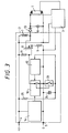
- the latch circuit 10 may be connected as shown in the modification illustrated in Figure 3, to respond to the voltage across a capacitor 24.
- the capacitor 24 is connected in series with a resistor 25 across the input terminals 4 and 5, and is shunted by a switch device 26.
- the switch device 26 which may involve a FET, is opened and closed in unison with the switching off and on of the latch circuit 10.
- the capacitor 24 charges via the resistor 25 while the latch circuit 10 is switched off and the switch device 26 is correspondingly open.
- the latch circuit 10 is switched on, and the consequent closing of the switch device 26 causes the capacitor 24 to be discharged.
- the switch device 26 opens allowing the capacitor 24 to charge again through the resistor 25. Charging is dependent on the input voltage, and with suitable choice of the values of the capacitor 24 and resistor 25, the voltage excursions across the capacitor 24 can mirror those across the resistor 9 to an adequate degree of accuracy for effective operation of the circuit.
Landscapes
- Engineering & Computer Science (AREA)
- Power Engineering (AREA)
- Discharge-Lamp Control Circuits And Pulse- Feed Circuits (AREA)
Applications Claiming Priority (2)
| Application Number | Priority Date | Filing Date | Title |
|---|---|---|---|
| GB939321912A GB9321912D0 (en) | 1993-10-23 | 1993-10-23 | Inverter circuits |
| GB9321912 | 1993-10-23 |
Publications (2)
| Publication Number | Publication Date |
|---|---|
| EP0650251A2 true EP0650251A2 (en) | 1995-04-26 |
| EP0650251A3 EP0650251A3 (enExample) | 1995-05-17 |
Family
ID=10744035
Family Applications (1)
| Application Number | Title | Priority Date | Filing Date |
|---|---|---|---|
| EP94307752A Withdrawn EP0650251A2 (en) | 1993-10-23 | 1994-10-21 | Inverter circuits |
Country Status (2)
| Country | Link |
|---|---|
| EP (1) | EP0650251A2 (enExample) |
| GB (1) | GB9321912D0 (enExample) |
Cited By (3)
| Publication number | Priority date | Publication date | Assignee | Title |
|---|---|---|---|---|
| EP0932248A1 (en) * | 1998-01-22 | 1999-07-28 | Rosemary Ann Ainslie | Method of harnessing a back-emf, and apparatus used in performing the method. |
| WO1999038247A1 (en) * | 1998-01-22 | 1999-07-29 | Ashby, Kevin, Peter | Harnessing a back emf |
| EP1885050A1 (de) * | 2006-08-01 | 2008-02-06 | Siemens Aktiengesellschaft | System und Verfahren zur Gatespannungsbestimmung eines Leistungsfeldeffekttransistors |
Family Cites Families (3)
| Publication number | Priority date | Publication date | Assignee | Title |
|---|---|---|---|---|
| US3820086A (en) * | 1972-05-01 | 1974-06-25 | Ibm | Read only memory(rom)superimposed on read/write memory(ram) |
| US4823070A (en) * | 1986-11-18 | 1989-04-18 | Linear Technology Corporation | Switching voltage regulator circuit |
| EP0613232B1 (de) * | 1993-02-24 | 1997-04-23 | Siemens Aktiengesellschaft | Sperrwandler-Schaltnetzteil mit einem Halbleiterschaltelement geringer Spannungsfestigkeit |
-
1993
- 1993-10-23 GB GB939321912A patent/GB9321912D0/en active Pending
-
1994
- 1994-10-21 EP EP94307752A patent/EP0650251A2/en not_active Withdrawn
Cited By (3)
| Publication number | Priority date | Publication date | Assignee | Title |
|---|---|---|---|---|
| EP0932248A1 (en) * | 1998-01-22 | 1999-07-28 | Rosemary Ann Ainslie | Method of harnessing a back-emf, and apparatus used in performing the method. |
| WO1999038247A1 (en) * | 1998-01-22 | 1999-07-29 | Ashby, Kevin, Peter | Harnessing a back emf |
| EP1885050A1 (de) * | 2006-08-01 | 2008-02-06 | Siemens Aktiengesellschaft | System und Verfahren zur Gatespannungsbestimmung eines Leistungsfeldeffekttransistors |
Also Published As
| Publication number | Publication date |
|---|---|
| GB9321912D0 (en) | 1993-12-15 |
| EP0650251A3 (enExample) | 1995-05-17 |
Similar Documents
| Publication | Publication Date | Title |
|---|---|---|
| US4275335A (en) | Constant light intensity electronic flash device | |
| CA2055392C (en) | Strobe circuit utilizing optocoupler in dc-to-dc converter | |
| EP0123030A1 (en) | Isolated power supply feedback | |
| JP2684601B2 (ja) | 低圧蛍光ランプのためのスイッチング制御回路と制御装置 | |
| EP0522574A1 (en) | Strobe alarm circuit | |
| KR890005601A (ko) | 정보 취급 및 제어 시스템과, 이 시스템에서 전기부하의 상태를 테스트 하는 방법 | |
| US5341082A (en) | Reverse current flow protector for electricity storage systems | |
| US5140226A (en) | Flashing warning light assembly | |
| JPS5918934B2 (ja) | 蓄電池充電装置 | |
| EP0650251A2 (en) | Inverter circuits | |
| GB2283136A (en) | Electric converter circuits | |
| EP1253810B1 (en) | Inverter circuits | |
| SE8103825L (sv) | Egenseker flamovervakningsanordning | |
| US6057648A (en) | Gas discharge lamp ballast with piezoelectric transformer | |
| US5446349A (en) | Strobe circuit utilizing optocoupler in DC-to-DC converter | |
| JPH0638367A (ja) | 突入電流防止回路 | |
| US4085353A (en) | Remote sensor trigger circuit | |
| GB2318655A (en) | Circuit for charging a capacitive load | |
| US5091688A (en) | Remotely switched voltage converter | |
| SU1758747A1 (ru) | Устройство дл управлени и защиты электрической нагрузки | |
| US5162702A (en) | Flashing light warning apparatus | |
| KR100295500B1 (ko) | 형광등의수명말기보호기능을갖춘전자식스타터 | |
| EP1411622A2 (en) | Inverter circuits | |
| SU847422A1 (ru) | Устройство защитного отключени элЕКТРОуСТАНОВКи | |
| RU2057661C1 (ru) | Устройство для обеспечения прерывистой работы сигнальной лампы |
Legal Events
| Date | Code | Title | Description |
|---|---|---|---|
| PUAI | Public reference made under article 153(3) epc to a published international application that has entered the european phase |
Free format text: ORIGINAL CODE: 0009012 |
|
| PUAL | Search report despatched |
Free format text: ORIGINAL CODE: 0009013 |
|
| AK | Designated contracting states |
Kind code of ref document: A2 Designated state(s): BE DE DK FR IT NL SE |
|
| AK | Designated contracting states |
Kind code of ref document: A3 Designated state(s): BE DE DK FR IT NL SE |
|
| STAA | Information on the status of an ep patent application or granted ep patent |
Free format text: STATUS: THE APPLICATION IS DEEMED TO BE WITHDRAWN |
|
| 18D | Application deemed to be withdrawn |
Effective date: 19951118 |