EP0638428B1 - Thermal printer with line-head - Google Patents
Thermal printer with line-head Download PDFInfo
- Publication number
- EP0638428B1 EP0638428B1 EP94401789A EP94401789A EP0638428B1 EP 0638428 B1 EP0638428 B1 EP 0638428B1 EP 94401789 A EP94401789 A EP 94401789A EP 94401789 A EP94401789 A EP 94401789A EP 0638428 B1 EP0638428 B1 EP 0638428B1
- Authority
- EP
- European Patent Office
- Prior art keywords
- memory
- printing
- register
- addressing
- activation
- Prior art date
- Legal status (The legal status is an assumption and is not a legal conclusion. Google has not performed a legal analysis and makes no representation as to the accuracy of the status listed.)
- Expired - Lifetime
Links
Images


Classifications
-
- B—PERFORMING OPERATIONS; TRANSPORTING
- B41—PRINTING; LINING MACHINES; TYPEWRITERS; STAMPS
- B41J—TYPEWRITERS; SELECTIVE PRINTING MECHANISMS, i.e. MECHANISMS PRINTING OTHERWISE THAN FROM A FORME; CORRECTION OF TYPOGRAPHICAL ERRORS
- B41J2/00—Typewriters or selective printing mechanisms characterised by the printing or marking process for which they are designed
- B41J2/315—Typewriters or selective printing mechanisms characterised by the printing or marking process for which they are designed characterised by selective application of heat to a heat sensitive printing or impression-transfer material
- B41J2/32—Typewriters or selective printing mechanisms characterised by the printing or marking process for which they are designed characterised by selective application of heat to a heat sensitive printing or impression-transfer material using thermal heads
- B41J2/35—Typewriters or selective printing mechanisms characterised by the printing or marking process for which they are designed characterised by selective application of heat to a heat sensitive printing or impression-transfer material using thermal heads providing current or voltage to the thermal head
- B41J2/355—Control circuits for heating-element selection
Definitions
- the present invention relates to a printing apparatus thermal line head, such as a fax machine or even a simple printer.
- a "line" thermal print head is used for printing almost all the points of a line simultaneously, which achieves high print speed.
- the head Used for example in a fax machine, the head has a large number of heating elements that print thermal under the command of as many activation bits. These bits are memorized, the time of printing a line, in a shift register with as many commanding outputs the heating elements individually. The points of the line could then be, if that is the case, be printed simultaneously, depending on the activation bits.
- the register controlling the heating elements is logically cut in blocks which are activated one after the other to print segments, or portions, of line together constituting the line to print.
- Such an arrangement multiplies the printing time by one line, which harms the intended goal which is, by a line impression, to obtain a high printing speed.
- the present invention aims to be able to increase this speed printing.
- a thermal printing apparatus with line head comprising a plurality of heating elements printers arranged to print successive lines of dots on a print medium dragged against the head, the heating elements being, via points memories of a printing register, controlled by individual activation means, apparatus characterized by the fact that the memory points are arranged to be individually deactivated one by one by the addressing means.
- each heating element can be modulated, that is to say that the head allows to restore black dots whose size depends on this duration and which appear, with their edges remaining white, like grays adjustable intensity.
- the write addressing means include a memory point addressing demultiplexer.
- the device may include means for controlling means write addressing arranged to receive input signals respectively representative of gray intensities of dots to print.
- the means of addressing and activation command can be arranged to simultaneously manage the heating time settings for several printing elements.
- the thermal printing apparatus of the invention comprises, in its first embodiment, a thermal head 1 shown in Figure 1, including a row of 1728 heating elements printing, generally referenced 2, cooperates with a ribbon thermal transfer printing ink not shown, applied to a print medium consisting of paper, driven scrolling against the head 1.
- the printing elements 2 are connected to a supply wire 3 at +24 volts and are controlled by individual amplifiers / switches 4 each controlled by its own activation bit stored in a memory point 6 here of the flip-flop type "D", from a print buffer register 5 to parallel inputs and outputs with an ordered row of 1728 such memory points 6.
- a demultiplexer circuit 10 comprises eleven address entries, referenced 11, and 1,728 outputs respectively connected to 1728 clock inputs 7 belonging respectively at 1728 memory points 6.
- the 1728 memory points 6 respectively comprise 1728 data bit inputs 8A connected to a common link 8. It an input 9 is here provided, connected to all the memory points 6, allowing the simultaneous reset of all, that is to say their forcing in the same predetermined state, here a logic level 0, says inactive, for which the heating elements 2 are not supplied with current through the amplifiers 4.
- the flip-flops "D" of the memory points 6 can for example be realized by means of integrated circuits, in TTL technology or CMOS, of type 7474 while demultiplexer 10 can, from even, be realized by means of several integrated circuits of the type 74154 or 74HC154 and a logic of selection of only one of them, acting on an address entry then serving as an entry for validation, the corresponding outputs of circuit 74 (HC) 154 being then unused.
- JK type flip-flops could have been provided, divider by two, not flip-flops "D", which would have avoided the need for data link 8 since each addressing of such a divider would be enough to make it change state.
- each memory point 6 is thus a bit activation of the heating elements 2, which can have two states, know an active state, here logic level 1, and an inactive state, here the logic level 0.
- the address memory point "three" returns to 0 during the period T3, while the address memory point "one” returns to 0 during the period T4.
- the impulses of order appearing from one period T1-T4 to the other pass to state 0, while in practice the data link 8 remains at the same level during each period T1-T4 and is read, by sampling, by an active edge, here falling, of the signal 7.
- the periods T1 -T4 are limited to a few tens of nanoseconds, which allows order all memory points 6 in good time less than the 10 milliseconds provided for by the standards for printing a line.
- Setting the duration of activation of each heating element 2 can thus be carried out by sending an order activation followed, after the desired duration, by sending a deactivation command resetting the bit to 0 activation.
- amplifiers 4 or the memory points 6 are inverters, or although link 9 allows to force all the bits of the printing register 5.
- all the bits of the register 5 are simultaneously set to the active state at the start line printing, even if it means deactivating them individually almost instantly if they correspond to white dots, or, if not, after the desired printing time.
- the adjustment of the activation time allows to modulate the amount of ink deposited on the paper at each point, i.e. get small black dots each surrounded of a remaining white area, which simulates grays, intensities independent from one point to another.
- the circuit 31 of FIG. 3 ensures the control of the multiplexer 10 by issuing the desired addresses in a timely manner.
- a reception link 32 provides a series of signals binaries representing numbers, coded in this example, arranged in the order of the dots to be printed, respectively representative of the gray intensities of the points from a line to to print.
- each number is proportional to the intensity of gray desired, the number "zero" indicating the presence of a point white and the coding corresponds to the classic binary coding.
- the circuit 31 stores this sequence of numbers in a register with offset 33 with parallel outputs then reads them successively in one partial scanning cycle by means of a multiplexer 34, addressed by a counter 35 advancing at the rate of a time base 39 of period Ti, until finding a number other than zero, indicating a gray to print.
- the address of counter 35 which corresponds to the relative position of the number in the row, i.e.
- the multiplexer 34 continues partial scan cycles of register 33 and a arithmetic circuit 37 of circuit 31 subtracts the value TA memorized of the value tj of the current instant, provided by the base 39, and compare the result to the corresponding coded number from register 33. If this number is reached or exceeded, a deactivation command is issued, as explained above.
- a printing register 45 controlling heating elements in the same way as the register 5 of the previous example, contains 1728 entries of memory point data 46 which through doors 44 are connected to as many outputs of an input register 43 containing, like register 33, a series of binary signals representing arranged numbers, also coded in this example, respectively representative of the gray intensities of the points a line to print.
- a control circuit 41 is connected by means of a reading 42 of circuit 41, to input register 43 and command the opening of a determined number of doors 44, of position determined, this number of doors being a function of the numbers coded read in register 43, as explained below.
- Hatched areas indicate blocks of bits transferred simultaneously, the position of the hatched areas of the register 43 corresponding to that of the hatched areas of the register 45, the presence of numbers other than zero, indicating gray, being marked by doubly blocks hatched. A coded number therefore corresponds to a bit of the same address of the printing register 45.
- Figure 5 shows in more detail the diagram of Figure 4.
- the output of the multiplexer 42 is connected to a transcoder circuit 47 which converts each coded number received into another number, not coded, of predetermined length, comprising bits at the head activation in state 1, in a number proportional to the intensity of the gray defined by the corresponding coded number, these non-coded numbers being stored in a memory 48.
- the memory 48 has not been shown in FIG. 4 and would therefore be interpose, with the transcoder circuit 47, between the outputs of the entry register 43 and doors 44.
- FIG. 6 represents three uncoded numbers, of five bits each, relating to three points 46-1, 46-2 and 46-5, the abscissa axis carrying the rank P of the memory points 46 and the ordinate axis carrying time t .
- Point 46-1 has only one bit in 1, so that gray will be light, while point 46-2, having a three-bit number in 1, will have a medium gray and point 46-5 , with 5 bits in 1, will be black because activated for the maximum duration X provided.
- the output of memory 48 also attacks a counter 49 which detects the presence of activation bits in 1 and emits a signal 50 when it reaches a predetermined value N.
- Signal 50 has the effect of stopping a common addressing counter 51 driving the multiplexer 42 and a demultiplexer 40, equivalent to the demultiplexer 10, connected at output to the printing register 45.
- a sequencer circuit 52 forces counter 51 to a determined address value, from value "a" at the beginning, and starts a cycle of a sequence of reading the first bits of each uncoded word from memory 48. If the bit read is in “1”, this "1" is copied into the memory point 46 of the same address through the demultiplexer 40. After N such copies, the counter 49 sends the stop signal 50, which stops any new sending of "1" to the printing register 45, and the AS address of the last 6 in 1 memory point is memorized by the circuit 52.
- Circuit 52 then resets counter 49 to "one" for start a new cycle, relating to the second bits of uncoded numbers from memory 48 and then sends a command to deactivate memory points 46, address "one" to AS, for which the second bit of the uncoded number is at state 0, which is the case for point 46-1.
- the bits of the line next to be printed are read in the input register 43, to start a new impression.
Abstract
Description
La présente invention concerne un appareil d'impression thermique à tête ligne, comme par exemple un télécopieur ou même une simple imprimante.The present invention relates to a printing apparatus thermal line head, such as a fax machine or even a simple printer.
Une tête d'impression thermique "ligne" sert à imprimer quasiment simultanément tous les points d'une ligne, ce qui permet d'atteindre une vitesse d'impression élevée.A "line" thermal print head is used for printing almost all the points of a line simultaneously, which achieves high print speed.
Utilisée par exemple dans un télécopieur, la tête comporte un grand nombre d'éléments chauffants qui effectuent l'impression thermique sous la commande d'autant de bits d'activation. Ces bits sont mémorisés, le temps de l'impression d'une ligne, dans un registre à décalage à autant de sorties commandant individuellement les éléments chauffants. Les points de la ligne pourraient être alors, si tel est le cas, être imprimés simultanément, en fonction des bits d'activation.Used for example in a fax machine, the head has a large number of heating elements that print thermal under the command of as many activation bits. These bits are memorized, the time of printing a line, in a shift register with as many commanding outputs the heating elements individually. The points of the line could then be, if that is the case, be printed simultaneously, depending on the activation bits.
Comme l'impression simultanée d'un grand nombre de points engendrerait une consommation de courant qui excéderait le débit autorisé de l'alimentation du télécopieur, le registre commandant les éléments chauffants est logiquement découpé en blocs qui sont activés les uns après les autres pour imprimer des segments, ou portions, de ligne constituant ensemble la ligne à imprimer.Like printing a large number of dots simultaneously would generate a current consumption which would exceed the authorized speed of the fax machine, the register controlling the heating elements is logically cut in blocks which are activated one after the other to print segments, or portions, of line together constituting the line to print.
Un tel agencement multiplie d'autant le temps d'impression d'une ligne, ce qui nuit au but visé qui est, par une impression ligne, d'obtenir une grande vitesse d'impression.Such an arrangement multiplies the printing time by one line, which harms the intended goal which is, by a line impression, to obtain a high printing speed.
La présente invention vise à pouvoir accroítre cette vitesse d'impression.The present invention aims to be able to increase this speed printing.
A cet effet, elle concerne un appareil d'impression thermique à tête ligne comportant une pluralité d'éléments chauffants d'impression agencés pour imprimer des lignes successives de points sur un support à imprimer entraíné en défilement contre la tête, les éléments chauffants étant, par l'intermédiaire de points mémoires d'un registre d'impression, commandés par des moyens d'activation individuels, appareil caractérisé par le fait que les points mémoires sont agencés pour être individuellement désactivés un à un par les moyens d'adressage.To this end, it relates to a thermal printing apparatus with line head comprising a plurality of heating elements printers arranged to print successive lines of dots on a print medium dragged against the head, the heating elements being, via points memories of a printing register, controlled by individual activation means, apparatus characterized by the fact that the memory points are arranged to be individually deactivated one by one by the addressing means.
On peut ainsi, lorsque le nombre de points à imprimer sur une ligne est limité, imprimer simultanément la totalité des points, alors que, dans l'art antérieur, une durée fixe était réservée à chaque bloc de commande, même s'il ne comportait qu'un seul point à imprimer.It is thus possible, when the number of dots to be printed on a line is limited, print all the dots simultaneously, whereas, in the prior art, a fixed period was reserved for each control block, even if it had only one point to print.
En outre, la durée de chauffage de chaque élément chauffant peut être modulée, c'est-à-dire que la tête permet de restituer des points noirs dont la taille dépend de cette durée et qui apparaissent, avec leur pourtour resté blanc, comme des gris d'intensité réglable.In addition, the heating time of each heating element can be modulated, that is to say that the head allows to restore black dots whose size depends on this duration and which appear, with their edges remaining white, like grays adjustable intensity.
Pour minimiser le nombre de liaisons d'adressage, il est préférable que les moyens d'adressage en écriture comportent un démultiplexeur d'adressage des points mémoire.To minimize the number of addressing links, it is preferable that the write addressing means include a memory point addressing demultiplexer.
Pour pourvoir imprimer des points noirs de taille inférieure à celle d'un pixel (élément d'image), équivalant à des gris, l'appareil peut comporter des moyens de commande des moyens d'adressage en écriture agencés pour recevoir en entrée des signaux respectivement représentatifs d'intensités de gris des points à imprimer. Mais, dans le même but, les moyens de commande d'adressage et d'activation peuvent être agencés pour gérer simultanément les réglages de durée de chauffage de plusieurs éléments d'impression. To print black dots smaller than that of a pixel (image element), equivalent to gray, the device may include means for controlling means write addressing arranged to receive input signals respectively representative of gray intensities of dots to print. But, for the same purpose, the means of addressing and activation command can be arranged to simultaneously manage the heating time settings for several printing elements.
L'invention sera mieux comprise à l'aide de la description suivante de deux formes de réalisation préférées de l'appareil d'impression thermique à tête ligne de l'invention, en référence au dessin annexé sur lequel :
- la figure 1 est un schéma par blocs de la tête d'impression dans la première forme de réalisation,
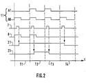
- la figure 2 est un diagramme des temps de signaux de commande de la tête d'impression de la figure 1,
- la figure 3 est un schéma par blocs de la tête d'impression ci-dessus et d'une logique de commande de cette tête,
- la figure 4 est un schéma par blocs de la seconde forme de réalisation,
- la figure 5 est un schéma plus détaillé que celui de la figure 4 et
- la figure 6 illustre l'évolution, en fonction du temps t, de l'état de points mémoire d'activation.
- FIG. 1 is a block diagram of the print head in the first embodiment,
- FIG. 2 is a diagram of the times of control signals of the print head of FIG. 1,
- FIG. 3 is a block diagram of the above print head and of a control logic for this head,
- FIG. 4 is a block diagram of the second embodiment,
- Figure 5 is a more detailed diagram than that of Figure 4 and
- FIG. 6 illustrates the evolution, as a function of time t, of the state of activation memory points.
L'appareil d'impression thermique de l'invention comporte, dans sa
première forme de réalisation, une tête thermique 1 représentée
sur la figure 1, dont une rangée de 1728 éléments chauffants
d'impression, globalement référencés 2, coopère avec un ruban
encreur d'impression par transfert thermique non représenté,
appliqué sur un support à imprimer constitué de papier, entraíné
en défilement contre la tête 1. Les éléments d'impression 2 sont
reliés à un fil d'alimentation 3 en +24 volts et sont commandés par
des amplificateurs/interrupteurs individuels 4 commandés chacun
par un bit d'activation propre mémorisé dans un point mémoire 6
ici du type bascule "D", d'un registre tampon d'impression 5 à
entrées et sorties parallèles comportant une rangée ordonnée de
1728 tels points mémoire 6. Un circuit démultiplexeur 10 comporte
onze entrées d'adresse, référencées 11, et 1728 sorties
respectivement reliées à 1728 entrées d'horloge 7 appartenant
respectivement aux 1728 points mémoires 6.The thermal printing apparatus of the invention comprises, in its
first embodiment, a thermal head 1 shown
in Figure 1, including a row of 1728 heating elements
printing, generally referenced 2, cooperates with a ribbon
thermal transfer printing ink not shown,
applied to a print medium consisting of paper, driven
scrolling against the head 1. The
Les 1728 points mémoires 6 comportent respectivement 1728
entrées de bit de donnée 8A reliées à une liaison commune 8. Il
est ici prévu une entrée 9, reliée à tous les points mémoire 6,
permettant la remise à zéro simultanée de tous, c'est-à-dire leur
forçage en un même état prédéterminé, ici un niveau logique 0, dit
inactif, pour lequel les éléments chauffants 2 ne sont pas
alimentés en courant à travers les amplificateurs 4.The 1728 memory points 6 respectively comprise 1728
data bit inputs 8A connected to a common link 8. It
an
Les bascules "D" des points mémoire 6 peuvent par exemple être
réalisées au moyen de circuits intégrés, en technologie TTL ou
CMOS, du type 7474 tandis que le démultiplexeur 10 peut, de
même, être réalisé au moyen de plusieurs circuits intégrés du type
74154 ou 74HC154 et d'une logique de sélection d'un seul d'entre
eux, agissant sur une entrée d'adresse servant alors d'entrée de
validation, les sorties correspondantes du circuit 74(HC)154 étant
alors inutilisées. Il aurait pu être prévu des bascules de type JK,
diviseur par deux, et non des bascules "D", ce qui aurait évité la
nécessité de la liaison de données 8 puisque chaque adressage
d'une telle bascule diviseur suffirait à la faire changer d'état.The flip-flops "D" of the memory points 6 can for example be
realized by means of integrated circuits, in TTL technology or
CMOS, of type 7474 while
Les circuits intégrés ci-dessus sont disponibles auprès des sociétés TEXAS INSTRUMENTS ou MOTOROLA.The above integrated circuits are available from TEXAS INSTRUMENTS or MOTOROLA companies.
Pour commander l'activation d'un élément chauffant 2, une
adresse correspondante dans la rangée est appliquée un court
instant aux entrées d'adresse 11, la liaison 8 ayant préalablement
été mise au niveau logique 1 (figure 2). La sortie du
démultiplexeur 10 reliée à l'entrée d'horloge 7 du point-mémoire 6
de l'élément chauffant 2 considéré fournit une impulsion pendant la
durée d'application de l'adresse aux entrées d'adresse 11, ce qui a
pour effet d'ouvrir une porte, non représentée, d'activation
individuelle d'un élément chauffant 2, qui lit le niveau logique de la
liaison de donnée 8 et commande la mémorisation, dans le point
mémoire 6 concerné, d'un bit ayant le niveau logique 1 présent sur
la liaison de donnée 8.To control the activation of a
La désactivation d'un point mémoire 6 s'effectue de même, la liaison 8 étant alors mise au niveau logique 0.The deactivation of a memory point 6 is carried out in the same way, the link 8 is then brought to logic level 0.
Le bit contenu dans chaque point mémoire 6 est ainsi un bit
d'activation des éléments chauffants 2, qui peut avoir deux états, à
savoir un état actif, ici le niveau logique 1, et un état inactif, ici le
niveau logique 0.The bit contained in each memory point 6 is thus a bit
activation of the
Ainsi, sur la figure 2, qui est un diagramme temporel des signaux
ci-dessus, le point mémoire 6 d'adresse "un" est adressé, un court
instant à l'intérieur d'une période T1 d'une suite Ti (i entier = 1 à
P), en mettant à 1 le bit d'adresse de poids faible A0 appliqué aux
entrées d'adresse 11, les autres bits, non tous représentés, étant
au niveau 0, ce qui engendre une impulsion sur l'entrée d'horloge
7 du point mémoire 6 d'adresse "un", dont le niveau logique, ou
état, est représenté par le signal 21.So in Figure 2, which is a time diagram of the signals
above, the memory point 6 of address "one" is addressed, a short
instant within a period T1 of a sequence Ti (i integer = 1 to
P), by setting the least significant address bit A0 applied to the
Pendant la période suivante T2, un autre point mémoire 6, ici
d'adresse "trois", est adressé, les deux bits d'adresse de poids
faible, A0 et A1, passant au niveau 1 pour fournir l'adresse binaire
11, soit trois en décimal. Le signal 23 représente le niveau logique
du bit contenu dans le point mémoire d'adresse "trois". Les états
initiaux des points mémoire 6 ont ici été supposés être l'état 0.During the following period T2, another memory point 6, here
address "three", is addressed, the two address bits of weight
weak, A0 and A1, passing to level 1 to provide the
Dans cet exemple, le point mémoire d'adresse "trois" repasse à 0 lors de la période T3, tandis que le point mémoire d'adresse "un" repasse à 0 à la période T4. Il y a ainsi gestion simultanée, ou entrelacée, de plusieurs points mémoire 6, grâce au partage du temps t en tranches ou périodes Ti.In this example, the address memory point "three" returns to 0 during the period T3, while the address memory point "one" returns to 0 during the period T4. There is thus simultaneous, or interleaved, management of several memory points 6, by sharing the time t into slices or periods Ti.
On comprendra que, dans un but de clarté, les impulsions de
commande apparaissant d'une période T1-T4 à l'autre repassent à
l'état 0, alors qu'en pratique la liaison de donnée 8 reste au même
niveau pendant chaque période T1-T4 et est lue, par
échantillonnage, par un front actif, ici descendant, du signal
d'horloge 7. De ce fait, les périodes T1 -T4 sont limitées à
quelques dizaines de nanosecondes, ce qui permet de
commander l'ensemble des points mémoire 6 en un temps bien
moindre que les 10 millisecondes prévues par les normes pour
l'impression d'une ligne.It will be understood that, for the sake of clarity, the impulses of
order appearing from one period T1-T4 to the other pass to
state 0, while in practice the data link 8 remains at the same
level during each period T1-T4 and is read, by
sampling, by an active edge, here falling, of the
Le réglage de la durée d'activation de chaque élément chauffant
2 peut ainsi être effectué par l'envoi d'une commande
d'activation suivi, après la durée voulue, de l'envoi d'une
commande de désactivation faisant repasser à 0 le bit
d'activation. Il aurait pu, de même, être prévu que les
amplificateurs 4 ou les points mémoires 6 soient inverseurs, ou
encore que la liaison 9 permette de forcer à 1 tous les bits du
registre d'impression 5. Dans ce cas, tous les bits du registre
d'impression 5 sont mis simultanément à l'état actif en début
d'impression de ligne, quitte à les désactiver individuellement
quasi instantanément s'ils correspondent à des points blancs,
ou, sinon, après la durée d'impression voulue.Setting the duration of activation of each
Le réglage de la durée d'activation des éléments chauffants 2
permet de choisir la température atteinte par ceux-ci, ainsi que le
temps de la diffusion thermique vers l'encre et le temps de
transfert lorsque l'encre a fondu.Setting the duration of activation of the
De ce fait, le réglage de la durée d'activation permet de moduler la quantité d'encre déposée sur le papier en chaque point, c'est-à-dire d'obtenir des points noirs de taille réduite entourés chacun d'une zone blanche restante, ce qui simule des gris, d'intensités indépendantes d'un point à l'autre. Therefore, the adjustment of the activation time allows to modulate the amount of ink deposited on the paper at each point, i.e. get small black dots each surrounded of a remaining white area, which simulates grays, intensities independent from one point to another.
Le circuit 31 de la figure 3, assure la commande du multiplexeur
10 en émettant les adresses voulues en temps opportun. Pour
cela, une liaison de réception 32 fournit une suite de signaux
binaires représentant des nombres, codés dans cet exemple,
rangés selon l'ordre des points à imprimer, respectivement
représentatifs des intensités de gris des points d'une ligne à
imprimer.The
Dans cet exemple, chaque nombre est proportionnel à l'intensité
de gris voulue, le nombre "zéro" indiquant la présence d'un point
blanc et le codage correspond au codage binaire classique. Le
circuit 31 mémorise cette suite de nombres dans un registre à
décalage 33 à sorties parallèles puis les lit successivement en un
cycle de balayage partiel au moyen d'un multiplexeur 34, adressé
par un compteur 35 avançant au rythme d'une base de temps 39 de
période Ti, jusqu'à trouver un nombre différent de zéro, indiquant
un gris à imprimer. L'adresse du compteur 35, qui correspond à la
position relative du nombre dans la rangée, c'est-à-dire la position
ou adresse du point mémoire 6 considéré, est appliquée aux
entrées d'adresse 11 du démultiplexeur 10, tandis que la liaison 8
est mise au niveau 1 par le circuit 31, pour activer le point
mémoire 6 correspondant, comme expliqué ci-dessus. Le
processus se poursuit jusqu'au dernier nombre. Les instants
d'activation des points mémoires 6, fournis par la base de temps
39, pourraient être mémorisés avec chaque nombre du registre 33,
mais dans ce cas, étant très proches, seul l'instant TA de la
dernière activation est noté.In this example, each number is proportional to the intensity
of gray desired, the number "zero" indicating the presence of a point
white and the coding corresponds to the classic binary coding. The
Pour la désactivation des éléments chauffants 6, le multiplexeur
34 poursuit des cycles de balayage partiel du registre 33 et un
circuit arithmétique 37 du circuit 31 soustrait la valeur TA
mémorisée de la valeur tj de l'instant en cours, fournie par la base
de temps 39, et compare le résultat au nombre codé correspondant
du registre 33. Au cas où ce nombre est atteint ou dépassé, une
commande de désactivation est émise, comme expliqué ci-dessus. For deactivation of the heating elements 6, the
Dans la seconde forme de réalisation représentée
schématiquement sur la figure 4, un registre d'impression 45,
commandant des éléments chauffants de la même façon que le
registre 5 de l'exemple précédent, comporte 1728 entrées de
données de points mémoire 46 qui, à travers des portes 44 sont
reliées à autant de sorties d'un registre d'entrée 43 contenant,
comme le registre 33, une suite de signaux binaires représentant
des nombres rangés, eux aussi codés dans cet exemple,
respectivement représentatifs des intensités de gris des points
d'une ligne à imprimer.In the second embodiment shown
schematically in FIG. 4, a
Un circuit de commande 41 est relié au moyen d'un circuit de
lecture 42 du circuit 41, au registre d'entrée 43 et commande
l'ouverture d'un nombre déterminé de portes 44, de position
déterminée, ce nombre de portes étant fonction des nombres
codés lus dans le registre 43, comme expliqué plus loin.A
Les zones hachurées indiquent des blocs de bits transférés
simultanément, la position des zones hachurées du registre 43
correspondant à celle des zones hachurées du registre
d'impression 45, la présence de nombres différents de zéro,
indiquant des gris, étant marquée par des blocs doublement
hachurés. A un nombre codé correspond donc un bit de même
adresse du registre d'impression 45.Hatched areas indicate blocks of bits transferred
simultaneously, the position of the hatched areas of the
La figure 5 montre de façon plus détaillée le schéma de la figure 4.
Le circuit de lecture 42 est un multiplexeur relié aux M sorties du
registre d'entrée 43, avec M = 1728 fois le nombre de bits de
chaque nombre codé.Figure 5 shows in more detail the diagram of Figure 4.
The
Comme les nombres du registre 43 sont codés dans cet exemple,
la sortie du multiplexeur 42 est reliée à un circuit transcodeur 47
qui convertit chaque nombre codé reçu en un autre nombre, non
codé, de longueur prédéterminée, comportant en tête des bits
d'activation à l'état 1, en nombre proportionnel à l'intensité du gris
définie par le nombre codé correspondant, ces nombres non codés
étant mémorisés dans une mémoire 48. Pour la clarté, la mémoire
48 n'a pas été représentée sur la figure 4 et serait donc à
interposer, avec le circuit transcodeur 47, entre les sorties du
registre d'entrée 43 et les portes 44.As the numbers in
La figure 6 représente trois nombres non codés, de cinq bits chacun, relatifs à trois points 46-1, 46-2 et 46-5, l'axe des abscisses portant le rang P des points mémoire 46 et l'axe des ordonnées portant le temps t. Le point 46-1 n'a qu'un bit en 1, si bien que le gris sera clair, tandis que le point 46-2, ayant un nombre à trois bits en 1, aura un gris moyen et le point 46-5, avec 5 bits en 1, sera noir car activé pendant la durée maximale X prévue.FIG. 6 represents three uncoded numbers, of five bits each, relating to three points 46-1, 46-2 and 46-5, the abscissa axis carrying the rank P of the memory points 46 and the ordinate axis carrying time t . Point 46-1 has only one bit in 1, so that gray will be light, while point 46-2, having a three-bit number in 1, will have a medium gray and point 46-5 , with 5 bits in 1, will be black because activated for the maximum duration X provided.
La sortie de la mémoire 48 attaque aussi un compteur 49 qui
détecte la présence de bits d'activation en 1 et émet un signal
d'arrêt 50 lorsqu'il atteint une valeur prédéterminée N. Le signal 50
a pour effet d'arrêter un compteur d'adressage 51 commun pilotant
le multiplexeur 42 et un démultiplexeur 40, équivalent du
démultiplexeur 10, relié en sortie au registre d'impression 45.The output of
Après écriture complète de la mémoire 48, un circuit séquenceur
52 force le compteur 51 à une valeur d'adresse déterminée, de
valeur "un" au début, et entame un cycle d'une séquence de
lecture des premiers bits de chaque mot non codé de la mémoire
48. Si le bit lu est en "1", ce "1" est recopié dans le point mémoire
46 de même adresse à travers le démultiplexeur 40. Après N telles
recopies, le compteur 49 émet le signal d'arrêt 50, ce qui arrête
tout nouvel envoi de "1" vers le registre d'impression 45, et
l'adresse AS du dernier point mémoire 6 en 1 est mémorisée par le
circuit 52. Le circuit 52 remet ensuite à "un" le compteur 49 pour
recommencer un nouveau cycle, relatif aux deuxièmes bits des
nombres non codés de la mémoire 48 et, alors, envoie une
commande de désactivation des points mémoire 46, d'adresse "un"
à AS, pour lesquels le deuxième bit du nombre non codé est à
l'état 0, ce qui est le cas pour le point 46-1. After complete writing of
D'autres cycles suivants, partant de l'adresse "un", permettent de
traiter les bits suivants des mêmes nombres non codés, ce qui, à
la fin, assure la désactivation des éléments chauffants 46
d'adresse "un" à AS. D'autres telles séquences de cycles, dont la
première commence à l'adresse AS+1, permettent de commander
successivement des blocs de taille variable (figure 4) comportant
des ensembles de N points mémoire 46 à l'état activé, dont deux
sont, comme indiqué, représentés à chaque fois sur la figure 4,
séparés par un nombre quelconque de points mémoire 46 à l'état
inactif. L'écriture par le démultiplexeur 40 s'effectue ainsi sous la
commande des moyens d'adressage (42, 49) puisque c'est le
compteur 49 qui détermine, par le signal d'arrêt 50, les adresses
extrêmes de chaque bloc de bits.Other following cycles, starting from the address "one", make it possible to
process the following bits of the same uncoded numbers, which, at
the end, deactivates the
Après écriture du dernier point noir de la ligne, les bits de la ligne
suivante à imprimer sont lus dans le registre d'entrée 43, pour
entamer une nouvelle impression.After writing the last black point of the line, the bits of the line
next to be printed are read in the
Claims (8)
- Thermal printer with line-head comprising a plurality of heating printing elements (2) arranged in order to print successive lines of dots on a printing support moved against the head (1), heating elements being, through the intermediary of memory points (6; 46) of a printing register (5; 45), controlled by individual activation means (7, 8), which printer is characterised by the fact that the memory points (6; 46) are arranged in order to be individually deactivated one by one by the addressing means (10; 40).
- Printer according to Claim 1, in which the writing addressing means comprise a demultiplexer (10; 40) for addressing memory points (6; 46).
- Printer according to one of Claims 1 and 2, in which the printing register (5; 45) comprises an input (9) for controlling the forcing of memory points (6) into the same predetermined state.
- Printer according to one of Claims 1 to 3, in which means (31; 41; 47, 48, 49, 51) are provided for controlling the writing addressing means (40) arranged to receive at the input signals respectively representative of the intensities of grey of the dots to be printed.
- Printer according to one of Claims 1 to 3, in which means (31) are provided for controlling the writing addressing means (10) and the activation control means (7, 8) comprise a connection (8) connected to the memory points (6) of the register (5).
- Printer according to one of Claims 4 and 5, in which the addressing and activation control means (31; 41) are arranged to simultaneously manage the regulations of the duration of heating of several printing elements (2).
- Printer according to one of Claims 4 to 6, in which reading addressing means (42, 49, 51) are provided arranged for reading, in an input memory (43; 48), a predetermined number of activation bits at an active state of a line to be printed and the means (51; 52) for controlling the writing addressing means (40) are arranged in order to select said activation bits under the command of the reading addressing means (42, 49, 51) and for controlling the transfer of said activation bits, from the input memory (43) to the printing register (45).
- Printer according to Claim 7, in which a counter (51) is provided for controlling the reading addressing means (42) and the writing addressing means (40) simultaneously.
Applications Claiming Priority (2)
| Application Number | Priority Date | Filing Date | Title |
|---|---|---|---|
| FR9309611 | 1993-08-04 | ||
| FR9309611A FR2708524B1 (en) | 1993-08-04 | 1993-08-04 | Line head thermal printing apparatus. |
Publications (2)
| Publication Number | Publication Date |
|---|---|
| EP0638428A1 EP0638428A1 (en) | 1995-02-15 |
| EP0638428B1 true EP0638428B1 (en) | 1999-02-17 |
Family
ID=9449938
Family Applications (1)
| Application Number | Title | Priority Date | Filing Date |
|---|---|---|---|
| EP94401789A Expired - Lifetime EP0638428B1 (en) | 1993-08-04 | 1994-08-03 | Thermal printer with line-head |
Country Status (6)
| Country | Link |
|---|---|
| US (1) | US5748220A (en) |
| EP (1) | EP0638428B1 (en) |
| AT (1) | ATE176770T1 (en) |
| DE (1) | DE69416551T2 (en) |
| ES (1) | ES2129111T3 (en) |
| FR (1) | FR2708524B1 (en) |
Families Citing this family (1)
| Publication number | Priority date | Publication date | Assignee | Title |
|---|---|---|---|---|
| DE102007025246A1 (en) * | 2007-05-30 | 2008-12-04 | Continental Automotive Gmbh | Method and apparatus for operating a thermal printer unit |
Family Cites Families (9)
| Publication number | Priority date | Publication date | Assignee | Title |
|---|---|---|---|---|
| US4284876A (en) * | 1979-04-24 | 1981-08-18 | Oki Electric Industry Co., Ltd. | Thermal printing system |
| FR2459591A1 (en) * | 1979-06-19 | 1981-01-09 | Amicel Jean Claude | METHOD AND DEVICE FOR FAXING WHITE HOPPING |
| JPS58175677A (en) * | 1981-11-09 | 1983-10-14 | Toshiba Corp | Method for driving heat sensitive head |
| JPS6044371A (en) * | 1983-08-20 | 1985-03-09 | Ricoh Co Ltd | Driving method for thermal head |
| JPS6342874A (en) * | 1986-08-08 | 1988-02-24 | Fujitsu Ltd | Printer |
| JP2575304B2 (en) * | 1987-03-06 | 1997-01-22 | イーストマン・コダック アジア・パシフィック株式会社 | Heating element driving device for thermal transfer printing head |
| US4746941A (en) * | 1987-10-13 | 1988-05-24 | Eastman Kodak Company | Dot printer with token bit selection of data latching |
| JPH0379377A (en) * | 1989-08-23 | 1991-04-04 | Seiko Instr Inc | Printing rate correction circuit for printer |
| US5053790A (en) * | 1990-07-02 | 1991-10-01 | Eastman Kodak Company | Parasitic resistance compensation for thermal printers |
-
1993
- 1993-08-04 FR FR9309611A patent/FR2708524B1/en not_active Expired - Fee Related
-
1994
- 1994-08-03 ES ES94401789T patent/ES2129111T3/en not_active Expired - Lifetime
- 1994-08-03 DE DE69416551T patent/DE69416551T2/en not_active Expired - Lifetime
- 1994-08-03 EP EP94401789A patent/EP0638428B1/en not_active Expired - Lifetime
- 1994-08-03 AT AT94401789T patent/ATE176770T1/en not_active IP Right Cessation
- 1994-08-04 US US08/285,949 patent/US5748220A/en not_active Expired - Fee Related
Also Published As
| Publication number | Publication date |
|---|---|
| FR2708524A1 (en) | 1995-02-10 |
| ATE176770T1 (en) | 1999-03-15 |
| ES2129111T3 (en) | 1999-06-01 |
| US5748220A (en) | 1998-05-05 |
| FR2708524B1 (en) | 1995-09-29 |
| EP0638428A1 (en) | 1995-02-15 |
| DE69416551D1 (en) | 1999-03-25 |
| DE69416551T2 (en) | 1999-09-23 |
Similar Documents
| Publication | Publication Date | Title |
|---|---|---|
| EP0023267B1 (en) | Printer control device | |
| FR2522911A1 (en) | ELECTRONIC DEVICE FOR CONTROLLING A THERMAL PRINTER FROM TELEVISION SIGNALS FOR REPRODUCING A FIXED TELEVISION IMAGE ON PAPER | |
| US5327165A (en) | Electronic printing system for imaging thermally sensitive paper | |
| FR2520532A1 (en) | THERMAL HEAD CONTROL DEVICE FOR THERMAL PRINTER | |
| EP0028957B1 (en) | Shade intensity reproducing device using a thermal print head, and thermal-printing system comprising such a device | |
| EP0638428B1 (en) | Thermal printer with line-head | |
| KR920000495A (en) | Thermal Video Printer with Temperature Compensation Improves Color Density | |
| EP0249523B1 (en) | Method of and apparatus for operating a thermal printing head | |
| US5548319A (en) | Gradation data method processing including repeated reading and recording of high density data | |
| JP2896249B2 (en) | Printer recording head drive | |
| EP0638429B1 (en) | Method for controlling the line head of a thermal printing apparatus and associated printer | |
| FR2558414A1 (en) | RECORDING APPARATUS | |
| KR940012270A (en) | Optical scanning device that applies laser beam on image surface to record image data in dots | |
| JP2516238B2 (en) | Thermal transfer recorder | |
| JP2838015B2 (en) | Print head | |
| JPH0260759A (en) | Thermal sensitive type printing head and controller thereof and these thermal sensitive type printing aggregate | |
| JPH02217266A (en) | Density gradation-type thermal printer | |
| JP2930088B2 (en) | Gradation recording method of thermal recording device | |
| JPS58151774A (en) | Recorder of gradation | |
| JP2927395B2 (en) | How to apply the energizing pulse to the thermal head | |
| JPH06286198A (en) | Thermal head drive controller | |
| AU680033B2 (en) | Thermal line-printer head | |
| FR2816428A1 (en) | Driver card for ink-jet printing heads, comprises microprocessor, memories, field programmable gate array and plugable electronic modules which are specific to particular types of printing head | |
| JP3034151B2 (en) | Thermal head drive controller | |
| KR960003973A (en) | Thermal transfer head and laser sublimation thermal transfer printer device using the same |
Legal Events
| Date | Code | Title | Description |
|---|---|---|---|
| PUAI | Public reference made under article 153(3) epc to a published international application that has entered the european phase |
Free format text: ORIGINAL CODE: 0009012 |
|
| AK | Designated contracting states |
Kind code of ref document: A1 Designated state(s): AT BE CH DE DK ES FR GB GR IE IT LI LU MC NL PT SE |
|
| 17P | Request for examination filed |
Effective date: 19950505 |
|
| 17Q | First examination report despatched |
Effective date: 19961129 |
|
| GRAG | Despatch of communication of intention to grant |
Free format text: ORIGINAL CODE: EPIDOS AGRA |
|
| GRAG | Despatch of communication of intention to grant |
Free format text: ORIGINAL CODE: EPIDOS AGRA |
|
| GRAH | Despatch of communication of intention to grant a patent |
Free format text: ORIGINAL CODE: EPIDOS IGRA |
|
| GRAH | Despatch of communication of intention to grant a patent |
Free format text: ORIGINAL CODE: EPIDOS IGRA |
|
| GRAA | (expected) grant |
Free format text: ORIGINAL CODE: 0009210 |
|
| AK | Designated contracting states |
Kind code of ref document: B1 Designated state(s): AT BE CH DE DK ES FR GB GR IE IT LI LU MC NL PT SE |
|
| PG25 | Lapsed in a contracting state [announced via postgrant information from national office to epo] |
Ref country code: SE Free format text: THE PATENT HAS BEEN ANNULLED BY A DECISION OF A NATIONAL AUTHORITY Effective date: 19990217 Ref country code: NL Free format text: LAPSE BECAUSE OF FAILURE TO SUBMIT A TRANSLATION OF THE DESCRIPTION OR TO PAY THE FEE WITHIN THE PRESCRIBED TIME-LIMIT Effective date: 19990217 Ref country code: IT Free format text: LAPSE BECAUSE OF FAILURE TO SUBMIT A TRANSLATION OF THE DESCRIPTION OR TO PAY THE FEE WITHIN THE PRESCRIBED TIME-LIMIT;WARNING: LAPSES OF ITALIAN PATENTS WITH EFFECTIVE DATE BEFORE 2007 MAY HAVE OCCURRED AT ANY TIME BEFORE 2007. THE CORRECT EFFECTIVE DATE MAY BE DIFFERENT FROM THE ONE RECORDED. Effective date: 19990217 Ref country code: GR Free format text: LAPSE BECAUSE OF NON-PAYMENT OF DUE FEES Effective date: 19990217 Ref country code: AT Free format text: LAPSE BECAUSE OF FAILURE TO SUBMIT A TRANSLATION OF THE DESCRIPTION OR TO PAY THE FEE WITHIN THE PRESCRIBED TIME-LIMIT Effective date: 19990217 |
|
| REF | Corresponds to: |
Ref document number: 176770 Country of ref document: AT Date of ref document: 19990315 Kind code of ref document: T |
|
| REG | Reference to a national code |
Ref country code: CH Ref legal event code: EP |
|
| REG | Reference to a national code |
Ref country code: IE Ref legal event code: FG4D Free format text: FRENCH |
|
| REF | Corresponds to: |
Ref document number: 69416551 Country of ref document: DE Date of ref document: 19990325 |
|
| PG25 | Lapsed in a contracting state [announced via postgrant information from national office to epo] |
Ref country code: PT Free format text: LAPSE BECAUSE OF FAILURE TO SUBMIT A TRANSLATION OF THE DESCRIPTION OR TO PAY THE FEE WITHIN THE PRESCRIBED TIME-LIMIT Effective date: 19990517 Ref country code: DK Free format text: LAPSE BECAUSE OF FAILURE TO SUBMIT A TRANSLATION OF THE DESCRIPTION OR TO PAY THE FEE WITHIN THE PRESCRIBED TIME-LIMIT Effective date: 19990517 |
|
| REG | Reference to a national code |
Ref country code: ES Ref legal event code: FG2A Ref document number: 2129111 Country of ref document: ES Kind code of ref document: T3 |
|
| GBT | Gb: translation of ep patent filed (gb section 77(6)(a)/1977) |
Effective date: 19990511 |
|
| NLV1 | Nl: lapsed or annulled due to failure to fulfill the requirements of art. 29p and 29m of the patents act | ||
| PG25 | Lapsed in a contracting state [announced via postgrant information from national office to epo] |
Ref country code: LU Free format text: LAPSE BECAUSE OF NON-PAYMENT OF DUE FEES Effective date: 19990803 |
|
| PG25 | Lapsed in a contracting state [announced via postgrant information from national office to epo] |
Ref country code: LI Free format text: LAPSE BECAUSE OF NON-PAYMENT OF DUE FEES Effective date: 19990831 Ref country code: CH Free format text: LAPSE BECAUSE OF NON-PAYMENT OF DUE FEES Effective date: 19990831 Ref country code: BE Free format text: LAPSE BECAUSE OF NON-PAYMENT OF DUE FEES Effective date: 19990831 |
|
| PG25 | Lapsed in a contracting state [announced via postgrant information from national office to epo] |
Ref country code: IE Free format text: LAPSE BECAUSE OF NON-PAYMENT OF DUE FEES Effective date: 19991019 |
|
| REG | Reference to a national code |
Ref country code: IE Ref legal event code: FD4D |
|
| PLBE | No opposition filed within time limit |
Free format text: ORIGINAL CODE: 0009261 |
|
| STAA | Information on the status of an ep patent application or granted ep patent |
Free format text: STATUS: NO OPPOSITION FILED WITHIN TIME LIMIT |
|
| 26N | No opposition filed | ||
| BERE | Be: lapsed |
Owner name: SOC. D'APPLICATIONS GENERALES D'ELECTRICITE ET DE Effective date: 19990831 |
|
| PG25 | Lapsed in a contracting state [announced via postgrant information from national office to epo] |
Ref country code: MC Free format text: LAPSE BECAUSE OF NON-PAYMENT OF DUE FEES Effective date: 20000229 |
|
| REG | Reference to a national code |
Ref country code: CH Ref legal event code: PL |
|
| REG | Reference to a national code |
Ref country code: GB Ref legal event code: IF02 |
|
| REG | Reference to a national code |
Ref country code: FR Ref legal event code: TP Ref country code: FR Ref legal event code: CD Ref country code: FR Ref legal event code: CA |
|
| REG | Reference to a national code |
Ref country code: GB Ref legal event code: 732E Free format text: REGISTERED BETWEEN 20090319 AND 20090325 |
|
| REG | Reference to a national code |
Ref country code: GB Ref legal event code: 732E Free format text: REGISTERED BETWEEN 20090326 AND 20090401 |
|
| REG | Reference to a national code |
Ref country code: FR Ref legal event code: TP |
|
| REG | Reference to a national code |
Ref country code: FR Ref legal event code: TP Owner name: SAGEMCOM DOCUMENTS SAS, FR Effective date: 20111005 |
|
| REG | Reference to a national code |
Ref legal event code: R082 Ref country code: DE Ref document number: 69416551 Country of ref document: DE Representative=s name: , |
|
| REG | Reference to a national code |
Ref country code: DE Ref legal event code: R081 Ref document number: 69416551 Country of ref document: DE Owner name: SAGEMCOM SAS, FR Free format text: FORMER OWNER: SOCIETE D'APPLICATIONS GENERALES D'ELECTRICITE ET DE MECANIQUE SAGEM, PARIS, FR Effective date: 20111228 |
|
| REG | Reference to a national code |
Ref country code: DE Ref legal event code: R081 Ref document number: 69416551 Country of ref document: DE Owner name: SAGEMCOM SAS, FR Free format text: FORMER OWNER: SAGEM TELECOMMUNICATIONS S. A., PARIS, FR Effective date: 20130129 |
|
| PGFP | Annual fee paid to national office [announced via postgrant information from national office to epo] |
Ref country code: DE Payment date: 20130722 Year of fee payment: 20 Ref country code: ES Payment date: 20130809 Year of fee payment: 20 |
|
| PGFP | Annual fee paid to national office [announced via postgrant information from national office to epo] |
Ref country code: FR Payment date: 20130820 Year of fee payment: 20 Ref country code: GB Payment date: 20130725 Year of fee payment: 20 |
|
| REG | Reference to a national code |
Ref country code: DE Ref legal event code: R071 Ref document number: 69416551 Country of ref document: DE |
|
| REG | Reference to a national code |
Ref country code: GB Ref legal event code: PE20 Expiry date: 20140802 |
|
| PG25 | Lapsed in a contracting state [announced via postgrant information from national office to epo] |
Ref country code: DE Free format text: LAPSE BECAUSE OF EXPIRATION OF PROTECTION Effective date: 20140805 |
|
| REG | Reference to a national code |
Ref country code: ES Ref legal event code: FD2A Effective date: 20141120 |
|
| PG25 | Lapsed in a contracting state [announced via postgrant information from national office to epo] |
Ref country code: GB Free format text: LAPSE BECAUSE OF EXPIRATION OF PROTECTION Effective date: 20140802 |
|
| PG25 | Lapsed in a contracting state [announced via postgrant information from national office to epo] |
Ref country code: ES Free format text: LAPSE BECAUSE OF EXPIRATION OF PROTECTION Effective date: 20140804 |