EP0634841B1 - Glatte Spektrumsspreizung mit kleinem Spreizfaktor - Google Patents
Glatte Spektrumsspreizung mit kleinem Spreizfaktor Download PDFInfo
- Publication number
- EP0634841B1 EP0634841B1 EP94110910A EP94110910A EP0634841B1 EP 0634841 B1 EP0634841 B1 EP 0634841B1 EP 94110910 A EP94110910 A EP 94110910A EP 94110910 A EP94110910 A EP 94110910A EP 0634841 B1 EP0634841 B1 EP 0634841B1
- Authority
- EP
- European Patent Office
- Prior art keywords
- rate
- parallel
- clock signal
- bits
- input bit
- Prior art date
- Legal status (The legal status is an assumption and is not a legal conclusion. Google has not performed a legal analysis and makes no representation as to the accuracy of the status listed.)
- Expired - Lifetime
Links
Images


Classifications
-
- H—ELECTRICITY
- H04—ELECTRIC COMMUNICATION TECHNIQUE
- H04J—MULTIPLEX COMMUNICATION
- H04J13/00—Code division multiplex systems
- H04J13/0007—Code type
- H04J13/0022—PN, e.g. Kronecker
-
- H—ELECTRICITY
- H04—ELECTRIC COMMUNICATION TECHNIQUE
- H04B—TRANSMISSION
- H04B1/00—Details of transmission systems, not covered by a single one of groups H04B3/00 - H04B13/00; Details of transmission systems not characterised by the medium used for transmission
- H04B1/69—Spread spectrum techniques
- H04B1/707—Spread spectrum techniques using direct sequence modulation
-
- H—ELECTRICITY
- H04—ELECTRIC COMMUNICATION TECHNIQUE
- H04J—MULTIPLEX COMMUNICATION
- H04J13/00—Code division multiplex systems
- H04J13/10—Code generation
Definitions
- This invention relates to spectrum spreading which is preferable for use in a satellite communication network including earth stations equipped with small diameter antennas as in a VSAT satellite communication network. More particularly, this invention relates to a spectrum spreading method, a spectrum spreading device, and a spectrum spreading transmitter in each of which use is made of spectrum spreading of the type described.
- Satellite communications system and apparatus are disclosed in United States Patent No. 4,455,651 issued to Paul Baran and assigned to Equatorial Communications Company, California, the United States of America.
- This satellite communication network of Baran provides a low cost satellite communication network.
- a small diameter antenna is used in each earth station for transmission and reception of radio signals.
- a spectrum spreading technique is used on producing a transmission signal.
- transmission data are spectrum spread at a spreading factor, namely, a ratio of a chip rate to an input bit rate, of the order of 256 and then subjected to BPSK modulation for transmission as the transmission signal to a satellite station.
- the VSAT satellite communication network which is used in practice in the United States of America and elsewhere, in which the input bit rate is about 64 Kbps, and in which the earth station is equipped with an antenna of a diameter of 1 meter with a transmission power of about 1 watt, it is possible without the spectrum spreading technique to provide a communication channel capable of insuring a sufficiently excellent communication quality to satisfy the FCC (Federal Communications Commission) standards. With the antenna diameter reduced to about 0.5 m, the VSAT satellite communication network would satisfy the FCC standards if the spectrum spreading technique is resorted to so as to reduce a spectrum power density off an antenna axis.
- FCC Federal Communications Commission
- a band spreading factor (hereafter referred to simply as the spreading factor) of at most about five (from four to eight) is sufficient in theory because the antenna has a gain difference of 6 dB, namely, 20 log (1/0.5) dB.
- spreading codes "0000” and "1111" These spreading codes provide two emission line spectra.
- the spectrum spread signal can not have a smooth spectrum.
- Spreading codes “1010” and “0101” also provide emission line spectra. With these spreading codes, an unevenness results in the spectrum spread signal. With spreading codes “1100” and “0011”, emission line spectra again appear in the spectrum of the spectrum spread signal. When the spreading factor is four, there are ten other spreading codes. All of these spreading codes do not give a sufficiently smooth spectrum to the spectrum spread signal.
- US-A-5,204,877 discloses a spread spectrum modulation device in which transmission data are converted into parallel data by a serial-parallel converting circuit which are held by a latch circuit and assign upper digit addresses. Lower digit addresses in the memory are assigned by a counter.
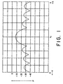
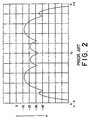
- a spectrum power density of a spectrum spread signal will first be described in order to facilitate an understanding of the present invention. It is assumed that a number of four is used as a spreading factor which is mentioned hereinabove and will become clear as the description proceeds.
- Fig. 1 the spectrum power density is illustrated for use as a reference without an input bit sequence subjected to spectrum spreading.
- the spectrum power density is scaled along the ordinate as indicated by P in dBm/Hz.
- the abscissa shows a frequency band of a BPSK modulated signal between a symbol rate X of plus four and minus four with a center frequency f0 at the center.
- the symbol rate of the BPSK modulated signal corresponds to an input bit rate of an input bit sequence from which the BPSK modulated signal is derived.
- nulls appear at 1.25 scales of the frequency band.
- a highest peak appears at the center frequency.
- Each of two adjacent peaks is 13 dB lower than the highest peak in the manner known in the art.
- the input bit sequence is spectrum spread with a spreading factor of four and then subjected to BPSK modulation.
- two maximum peaks appear on both sides of the center frequency.
- Next high peaks appear between the maximum peaks nearer to the center frequency.
- the maximum peaks have a height which is not appreciably different from the highest peak depicted in Fig. 1.
- the next high peaks are 9 dB lower than the maximum peaks.
- Figs. 1 and 2 it is understood that use of spectrum spreading reduces a peak to peak difference by 3 dB. It is desirable when the signal band is four times widened that the peak to peak difference should be reduced to one by four (by 6 dB). Use of the spreading factor of four, however, reduces the peak to peak difference only to 3 dB, namely, only to a half of the desired value. This makes it difficult to satisfy the FCC standards for the out of axis antenna radiation mentioned heretobefore. This is the reason why the spreading factor of 256 is used by Baran as described in the foregoing even at the cost of a possibly increased amount of interference.
- a spectrum spreading transmitter which comprises a spectrum spreading device according to a preferred embodiment of this invention.
- the spectrum spreading device is operable with a spreading factor N of four.
- the spectrum spreading device has a device input terminal 11, a shift clock input terminal 13, a chip clock input terminal 15, and a device output terminal 17.
- the device input terminal 11 is supplied with an input bit sequence IN of an input bit rate fs.
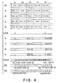
- the input bit sequence is a sequence of i-th through (i+4)-th and other bits D(i), D(i+1), ..., D(i+4), and so forth.
- the input bit sequence is delivered to a serial shift register 19 comprising first through fourth shift register stages A, B, C, and D in correspondence to the spreading factor of four.
- the register stages have first through fourth stage output terminals.
- a shift clock signal SCLK is supplied to the shift clock input terminal 13 at the input bit rate in synchronism with the input bit sequence.
- the shift clock signal defines the time slots for the input bit sequence and for the shift register 19 and is used as shift pulses in the shift register 19. It is possible to understand the shift clock input terminal 13 as shift clock generator means for generating the shift clock signal.
- a first counter 21 divides the shift clock signal by 1/4 or 1/N and produces a low rate clock signal LCLK of a lower rate fs/4.
- the first counter 21 therefore serves as a first divider for dividing the shift clock signal by 1/N to produce the low rate clock signal.
- the low rate clock signal is exemplified in Fig. 4 along a sixth row labelled LCLK with its clock pulses indicated by short upright arrows. It will be noted that the clock pulses are produced with a delay relative to the time slots depicted along the first row IN together with the bits D(i) and so on of the input bit sequence IN.
- the low rate clock signal is nevertheless in synchronism with the shift clock signal, because the shift clock signal is divided into the low rate clock signal.
- a memory unit 23 comprises first to fourth memory elements E, F, G, and H having first to fourth element output terminals, respectively.
- the low rate clock signal is supplied simultaneously to the first to the fourth memory elements to serve as load pulses at the lower rate.
- the first to the fourth memory elements are connected to the first through the fourth stage output terminals of the shift register 19, respectively. From the shift register 19, each shifted datum is stored in the memory unit 23 as a stored datum of first to fourth or n-th stored bits.
- the shifted data are transferred from the shift register 19 to the memory unit 23 once in four or N time slots, which may be called a longer time interval or slot.
- N time slots which may be called a longer time interval or slot.
- the (i-1)-th bit D(i-1) is transferred from the first register stage A to the first memory element E and kept in the first memory element in the manner depicted in Fig. 4 along a seventh row labelled E.
- the (i-2)-th through the (i-4)-th bits D(i-2), D(i-3), and D(i-4) are kept in the second to the fourth memory elements as illustrated along seventh to tenth rows labelled F, G, and H.
- the stored data are produced from the first to the fourth or the N-th element output terminals as N parallel bit sequences.
- the parallel bit sequences comprise N parallel bits into which the N consecutive bits of the input bit sequence are rearranged.
- a combination of the shift clock generator means (13), the shift register 19, the first divider (21), and the memory unit 23 is understood as series to parallel converter means for converting the input bit sequence into the N parallel bit sequences.
- Each longer time interval or slot is referred to simply as a time slot in connection with the parallel bit sequences and with the series to parallel converter means (13, 19, 21, 23).
- the row rate clock signal is supplied furthermore to a second counter 25 having a full count of 16, namely, N 2 . Loaded by each clock pulse of the row rate clock signal, the second counter 25 counts up from zero up to fifteen.
- the second counter 25 consequently serves as a second divider for dividing the row rate clock signal by sixteen or N 2 to produce a high rate clock signal HCLK at a higher rate of N 2 fs in synchronism with the row rate clock signal.
- the high rate clock signal is depicted along an eleventh row labelled HCLK by 0, 1, 2, ..., 15, 0, 1, ... . It is possible to supply the shift clock signal from the shift clock input terminal 13 directly to the second divider (25) in producing the high rate clock signal by division by N. Supply of the low rate clock signal is nevertheless preferred in order to insure synchronism between the high and the low rate clock signals.
- a selector 27 is depicted as a rotary switch merely for convenience of illustration and comprises first to fourth selector terminals 29(1), 29(2), 29(3), and 29(4) which will either collectively or individually designated by a simple reference numeral 29 without addition thereto of the suffixes enclosed with the parentheses.
- selector terminals 29 are supplied from the memory unit 23 with the first to the N-th stored bits.
- a selector element 31 is put into operation in response to the high rate clock signal to select the first to the fourth or the N-th selector terminals 29 cyclically four or N times while the first to the N-th stored bits are supplied to the selector terminals 29 from the first to the N-th element output terminals of the memory unit 23.
- the selector 27 produces a serial data sequence DS of serial data.
- Each serial datum comprises sixteen or N 2 bits in which the N parallel bits of each time slot of the shift register 19 are N times repeatedly arranged in the manner illustrated in Fig. 4 along a twelfth row labelled DS by bits D(i-4), D(i-3), D(i-2), D(i-1), D(i-4), D(i-3), D(i-2), ..., and D(i-1); or bits D(i), D(i+1), D(i+2), D(i+3), ... .
- the selector 27 serves as parallel to series converter means for converting the N parallel bit sequences into a series data sequence in cooperation with the second divider (25).
- the chip clock input terminal 15 is supplied with a chip clock signal CCLK of the chip rate fc which is equal to 4fs or Nfs.
- a spreading code generator (PN GEN) 33 Supplied with the high rate clock signal at a reset terminal R and with the chip clock signal, a spreading code generator (PN GEN) 33 generates spreading or psuedorandom (PN) codes PN of a code length of sixteen or N 2 bits at the higher clock rate.
- the spreading codes are repetitions of a partial code sequence C(0), C(1), C(2), C(3), ..., and C(15) depicted in Fig. 4 along a thirteenth or bottom row labelled PN.
- the code length of the spreading codes is N 2 bits long despite the fact that the spreading factor is equal to N.
- the high rate clock signal is used in order to keep the spreading codes in synchronism therewith.
- an Exclusive OR circuit 35 serves as spreader means for spectrum spreading the serial data sequence by the spreading codes to deliver a spectrum spread signal to the device output terminal 17.
- a modulator (MOD) 37 Connected to the device output terminal 17, a modulator (MOD) 37 generates a carrier signal and subjects the carrier signal to BPSK modulation by the spectrum spread signal to produce a BPSK modulated signal.
- a transmitter circuit (TX CKT) 39 produces a transmission signal.
- the transmission signal feeds an antenna 41 and is transmitted therefrom to a satellite station (not shown).
- the BPSK signal is produced by the modulator 27 with smooth spectrum spreading when use is made of the spectrum spreading device illustrated with reference to Figs. 3 and 4.
- the BPSK signal is possessed of a peak spectrum power density which is about 6 dB lower than the BPSK signal described in conjunction with Fig. 1 and about 3 dB lower than the BPSK signal described with reference to Fig. 2. This smooth spectrum is rendered possible because of the following reasons.
- the input bit sequence is not spectrum spread as it stands. Instead, the input bit sequence is converted eventually into the serial data signal in which each serial datum is a periodic function of a period of 1/4 or 1/N of the input bit rate fs.
- each serial datum is a periodic function of a period of 1/4 or 1/N of the input bit rate fs.
- this gives a randomness to the spectrum spread signal although the spreading factor is equal only to N or four.
- this makes it possible to use the spreading codes of the code length of sixteen or N 2 bits to provide a salient feature which can be achieved by spreading codes of a long code length.
- each bit of the input bit sequence has a bit structure of, for example, a predetermined number of binary bits. It is furthermore possible to use a spreading factor of only two.
Landscapes
- Engineering & Computer Science (AREA)
- Computer Networks & Wireless Communication (AREA)
- Signal Processing (AREA)
- Compression, Expansion, Code Conversion, And Decoders (AREA)
- Digital Transmission Methods That Use Modulated Carrier Waves (AREA)
- Synchronisation In Digital Transmission Systems (AREA)
- Other Investigation Or Analysis Of Materials By Electrical Means (AREA)
- Time-Division Multiplex Systems (AREA)
Claims (17)
- Verfahren zur Spektrumsspreizung einer Eingangsbitsequenz einer Eingangsbitrate in ein spektrumgespreiztes Signal einer Chip-Rate, die gleich N-mal der Eingangsbitrate ist, wobei N eine ganze Zahl repräsentiert, die gleich oder wenigstens zwei ist, mit den Schritten:Reihen-Parallel-Umwandlung der Eingangsbitsequenz in N parallele Bitsequenzen, mit N parallelen Bits, wobei N aufeinanderfolgende Bits der Eingangsbitsequenz in jedem längeren Zeitschlitz neu angeordnet werden, wobei der längere Zeitschlitz eine Dauer von N Zeitschlitzen der Eingangsbitsequenz hat;Paralel-Reihen-Umwandlung der parallelen Bitsequenzen in eine Reihendatensequenz von Reihendaten, wobei jedes Reihendatum N2 Bits enthält, wobei die N parallelen Bits jedes der Zeitschlitze N mal wiederholt angeordnet sind;Erzeugen von Spreizcodes mit einer Code-Länge von N2 Bits bei der Chiprate; und Spektrumsspreizen der Reihendatensequenz durch die Spreizcodes in das spektrumsgespreizte Signal.
- Verfahren nach Anspruch 1, wobei das Reihendatum N-fache Wiederholungen der N aufeinanderfolgenden Bits der Eingangsbitsequenz aufweist.
- Verfahren nach Anspruch 1, wobei:wobei der Parallel-Reihen-Umwandlungsschritt die Parallelbitsequenz in die Reihendatensequenz mit einer höheren Rate umwandelt, die gleich dem N-fachen der Eingangsbitrate ist.der Reihen-Parallel-Umwandlungsschritt die Eingangsbitsequenz in die parallelen Bitsequenzen umwandelt, wobei die Zeitschlitze bei einer niedrigeren Rate, die gleich der Eingangsbitrate geteilt durch N ist, defininiert sind;
- Verfahren nach Anspruch 3, wobei:wobei der Parallel-Reihen-Umwandlungsschritt die Schritte aufweist:der Reihen-Parallel-Umwandlungsschritt die Schritte aufweist:Erzeugen eines Schiebetaktsignals mit der Eingangsbitrate synchron mit der Eingangsbitsequenz;Verschieben der Eingangsbitsequenz durch das Schiebetaktsignal in ein Schieberegister, wobei die N aufeinanderfolgenden Bits als ein Schiebedatum verschoben werden;Erzeugen eines Taktsignals mit niedrigerer Rate mit der niedrigeren Rate synchron mit dem Schiebetaktsignal; undSpeichern des um das Signal mit der niedrigeren Rate verschobenen Datums als gespeichertes Datum, welches die N parallelen Bits und die parallelen Bitsequenzen mit der niedrigeren Rate bereitstellt; in einem SpeicherErzeugen eines Taktsignals mit höherer Rate mit der höheren Rate synchron mit dem Taktsignal mit niedrigerer Rate; undWählen des gespeicherten Datums in Antwort auf das Taktsignal mit höherer Rate, das N mal wiederholt wird, um das Reihendatum der Reihendatensequenz zu erzeugen.
- Verfahren nach Anspruch 1, weiterhin mit dem Schritt Modulieren eines Trägersignals mit dem Spektrumspreizsignal zu einem modulierten Signal und Übertragen des modulierten Signals als Übertragungssignal.
- Spektrumspreizvorrichtung zur Spektrumspreizung einer Eingangsbitsequenz einer Eingangsbitrate in ein Spektrumspreizsignal einer Chiprate, die gleich dem N-fachen der Eingangsbitrate ist, wobei N eine ganze Zahl repräsentiert, die gleich oder wenigstens zwei ist, mit Spreizmitteln (35) für die Spektrumspreizung eines Eingangssignals durch Spreizcodes in das Sprektrumsspreizsignal und gekennzeichnet durch:Reihen-Parallel-Wandlermittel (13, 19, 21, 23) die so angeordnet sind, dass sie die Eingangsbitsequenz in N parallele Bitsequenzen umwandeln, die N parallele Bits aufweisen, wobei N aufeinanderfolgende Bits der Eingangsbitsequenz in jedem längeren Zeitschlitz neu angeordnet sind, wobei der längere Zeitschlitz eine Dauer von N Zeitschlitzen der Eingangsbitsequenz hat;Parallel-Reihen-Wandlermittel (25, 27) zum Umwandeln der parallelen Bitsequenzen zur Verwendung als das Eingangssignal in eine Reihendatensequenz der Reihendaten, wobei jedes Reihendatum N2 Bits hat, wobei die N parallelen Bits jedes der Zeitschlitze N-fach wiederholt angeordnet sind; undCode-Generatormittel (15, 33) zum Erzeugen des Spreizcodes bei der Chiprate, wobei ihrer Codelänge N2 Bits verliehen sind.
- Spektrumspreizvorrichtung nach Anspruch 6, dadurch gekennzeichnet, dass:die Reihen-Parallel-Wandlermittel (13, 19, 21, 23) die Eingangsbitsequenz in die Parallelbitsequenz umwandeln, wobei die Zeitschlitze bei einer niedrigeren Rate definiert sind, die gleich der Eingangsbitrate geteilt durch N ist;die Parallel-Reihen-Wandlermittel (25, 27) die Parallelbitsequenzen in die Reihendatensequenz bei einer höheren Rate umwandeln, die gleich dem N-fachen der Eingangsbitrate ist.
- Spektrumspreizvorrichtung nach Anspruch 7, dadurch gekennzeichnet, dass:wobei die Parallel-Reihen-Wandlermittel (25, 27) aufweisen:die Reihen-Parallel-Wandlermittel (13, 19, 21, 23) aufweisen:Schiebetaktgeneratormittel (13) zum Erzeugen eines Schiebtaktsignals bei der Eingangsbitrate synchron mit der Eingangsbitsequenz;Schieberegistermittel (19), die auf das Schiebetaktsignal antworten, um die Eingangsbitsequenz mit den N aufeinanderfolgenden Bits, die als verschobenes Datum bei der Eingangsbitrate verschoben sind, zu verschieben;erste Teilermittel (21) zum Teilen des Schiebetaktsignals durch 1/N, um ein Taktsignal mit niedriger Rate bei der niedrigeren Rate zu erzeugen; undSpeichermittel (23) die auf das Taktsignal mit niedriger Rate antworten, um das verschobene Datum als ein gespeichertes Datum zu speichern, welches die N parallelen Bits bereitstellt und die Parallelbitsequenzen bei der niedrigeren Rate bereitstellt;wobei die Codegeneratormittel (15, 33) aufweisen:zweite Teilermittel (25) zum Teilen des Taktsignals mit niedriger Rate durch N2, um ein Taktsignal mit hoher Rate bei der höheren Rate herzustellen; undWählmittel (27), die auf das Taktsignal mit hoher Rate antworten, um das gespeicherte Datum N-mal wiederholt zu wählen, um das Reihendatum herzustellen und um die Reihendatensequenz bei der höheren Rate herzustellen;Chip-Taktgeneratormittel (15) zum Erzeugen eines Chip-Taktsignals mit der Chiprate; undeinen Codegenerator (33), der auf das Taktsignal mit hoher Rate und auf das Chip-Taktsignal antwortet, um die Spreizcodes mit der Codelänge synchron mit der Reihendatensequenz zu erzeugen.
- Spektrumspreizvorrichtung nach Anspruch 8, dadurch gekennzeichnet, dass:die Schieberegistermittel (19) aufweisen:erste bis N-te Registerstufen (A, B, ...) mit jeweils ersten bis N-ten Stufenausgangsanschlüssen;Mittel zum Zuführen der Eingangsbitsequenz Bit für Bit zu der ersten Registerstufe; Mittel, die auf das Schiebetaktsignal antworten, um die N aufeinanderfolgenden Bits von der ersten Registerstufe auf die N-ten Registerstufe als das verschobene Datum zu verschieben; undMittel, die auf das Schiebetaktsignal antworten, um die Parallelbitsequenzen von den ersten bis N-ten Stufenausgangsanschlüssen zu erzeugen.
- Spektrumspreizvorrichtung nach Anspruch 8, wobei die N parallelen Bits die ersten bis N-ten Bits sind, dadurch gekennzeichnet, dass die Speichermittel (23) aufweisen:erste bis N-te Speicherelemente (E, F, ...) mit jeweils ersten bis N-ten Elementausgangsanschlüssen;Mittel, die auf das Taktsignal mit niedriger Rate antworten, um die Parallelbitsequenz zu den ersten bis N-ten Speicherelementen zu leiten, um die ersten bis N-ten Bits simultan in den ersten bis N-ten Speicherelementen gleichzeitig als das gespeicherte Datum zu speichern; undMittel, die auf das Taktsignal mit niedriger Rate antworten, um das gespeicherte Datum von den ersten bis N-ten Elementausgangsanschlüssen N-mal wiederholt als die N parallelen Bits zu erzeugen und die Parallelbitsequenzen bei niedriger Rate zu erzeugen.
- Spektrumspreizvorrichtung nach Anspruch 10, wobei das gespeicherte Datum in den ersten bis N-ten Speicherelementen als jeweils erste bis N-te gespeicherte Bits gespeichert ist, dadurch gekennzeichnet, dass die Wählmittel (27) aufweisen:Wählelementmittel (31), die auf das Taktsignal mit hoher Rate antworten, um die ersten bis N-ten Elementausgangsanschlüsse zyklisch N-mal zu wählen, während die ersten bis N-ten gespeicherten Bits in den ersten bis N-ten Speicherelementen gespeichert werden; undMittel zum Erzeugen der N2 Bits, während die Wählelementmittel zyklisch die ersten bis N-ten Elementausgangsanschlüsse wählen, um die Reihendatensequenz bei der höheren Bitrate zu erzeugen.
- Spektrumspreizssender mit einer Spektrumspreizvorrichtung nach einem der Ansprüche 6 bis 11, weiterhin mit Modulatormitteln (37) zum Modulieren eines Trägersignals durch das Spektrumspreizsignal in ein moduliertes Signal und Sendermittel (39) zum Senden des modulierten Signals als das Sendesignal.
- Spektrumspreizsender nach Anspruch 12, dadurch gekennzeichnet, dass:die Reihen-Parallel-Wandlermittel (13, 19, 21, 23) die Eingangsbitsequenz in die Parallelbitsequenzen mit den Zeitschlitzen umwandeln, die bei einer niedrigeren Rate definiert sind, die gleich der Eingangsbitrate geteilt duch N ist;die Parallel-Reihen-Wandlermittel (23, 25) die Parallelbitsequenzen in die Reihendatensequenz mit einer höheren Rate umwandeln, die gleich dem N-fachen der Eingangsbitrate ist.
- Spektrumspreizsender nach Anspruch 13, dadurch gekennzeichnet, dass:wobei die Parallel-in-Reihen-Wandlermittel (25, 27) aufweisen:die Reihen-Parallel-Wandlermittel (13, 19, 21, 23) aufweisen:Schiebetaktgeneratormittel (13) zum Erzeugen eines Schiebetaktsignals bei der Eingangsbitrate synchron mit der Eingangsbitsequenz;Schieberegistermittel (19), die auf das Schiebetaktsignal antworten, um die Eingangsbitsequenz mit N aufeinanderfolgenden Bits zu verschieben, die als ein Schiebedatum mit der Eingangsbitrate verschoben werden;erste Teilermittel (21) zum Teilen des Schiebetaktsignals durch 1/N, um ein Taktsignal mit niedriger Rate mit der niedrigeren Rate zu erzeugen; undSpeichermittel (23), die auf das Taktsignal mit niedriger Rate antworten, um das verschobene Datum als ein gespeichertes Datum zu speichern, das die N parallelen Bits bereitstellt und das die Parallelbitsequenzen mit der niedrigeren Rate bereitstellt;wobei die Codegeneratormittel (15, 33) aufweisen:zweite Teilermittel (25) zum Teilen des Taktsignals mit niedriger Rate durch N2 um ein Taktsignal mit hoher Rate mit höherer Rate zu erzeugen; undWählmittel (27), die auf das Taktsignal mit hoher Rate antworten, um das gespeicherte Datum N-mal wiederholt zu wählen um das Reihendatum und die Reihendatensequenz mit der höheren Rate zu erzeugen;Chip-Taktgeneratormittel (15) zum Erzeugen eines Chip-Taktsignals mit der Chip-Rate; undeinen Codegenerator (33), der auf das Taktsignal mit hoher Rate und das Chip-Taktsignal antwortet, um die Spreizcodes mit der Codelänge synchron mit dem Reihendatensignal zu erzeugen.
- Spektrumspreizsender nach Anspruch 14, dadurch gekennzeichnet, dass die Schieberegistermittel (19) aufweisen:erste bis N-te Registerstufen (A, B, ...) mit jeweils ersten bis N-ten Stufenausgangsanschlüssen;Mittel zum Bit für Bit Zuführen der Eingangsbitssequenz zu der ersten Registerstufe; Mittel, die auf das Schiebetaktsignal antworten, um die N Verbindungsbits von der ersten Registerstufe auf die N-te Registerstufe als das verschobene Datum mit der niedrigeren Rate zu verschieben; undMittel, die auf das Schiebetaktsignal antworten, um die Parallelbitsequenzen von den ersten bis N-ten Stufenausgangsanschlüssen zu erzeugen.
- Spektrumspreizsender nach Anspruch 14, wobei N parallele Bits erste bis N-te Bits sind, dadurch gekennzeichnet, dass die Speichermittel (25, 27) aufweisen:erste bis N-te Speicherelemente (E, F, ...) mit jeweils ersten bis N-ten Elementausgansanschlüssen;Mittel, die auf das Taktsignal mit niedriger Rate antworten, um die parallelen Bitsignale zu den ersten bis N-ten Speicherelementen zu leiten, um die ersten bis N-ten Bits simultan in den ersten bis N-ten Speicherlementen als das gespeicherte Datum zu speichern; undMittel, die auf das Taktsignal mit niedriger Rate antworten, um das gespeicherte Datum von den ersten bis N-ten Elementausgangsanschlüssen als die N parallelen Bits zu erzeugen und um die Parallelbitsequenzen mit niedrigerer Rate zu erzeugen.
- Spektrumspreizsender nach Anspruch 16, wobei das gespeicherte Datum in den ersten bis N-ten Speicherelementen jeweils als erste bis N-ten gespeicherte Bits gespeichert ist, dadurch gekennzeichnet, dass die Wählmittel (27) aufweisen:Wählelementmittel (31), die auf das Taktsignal mit hoher Rate antworten, um die ersten bis N-ten Elementausgansanschlüsse zyklisch N-mal zu wählen, während die ersten bis N-ten gespeicherten Bits in den ersten N-ten Speicherelementen gespeichert werden; undMittel zum Erzeugen der N2 Bits, während die Wählelementmittel die ersten bis N-ten Elementausgangsanschlüssen zyklisch wählen, um die Reihendatumsequenz mit höherer Rate zu erzeugen.
Applications Claiming Priority (3)
| Application Number | Priority Date | Filing Date | Title |
|---|---|---|---|
| JP17351893 | 1993-07-14 | ||
| JP5173518A JP2508595B2 (ja) | 1993-07-14 | 1993-07-14 | スペクトラム拡散方式およびスペクトラム拡散送信機 |
| JP173518/93 | 1993-07-14 |
Publications (3)
| Publication Number | Publication Date |
|---|---|
| EP0634841A2 EP0634841A2 (de) | 1995-01-18 |
| EP0634841A3 EP0634841A3 (de) | 1997-07-30 |
| EP0634841B1 true EP0634841B1 (de) | 2005-12-21 |
Family
ID=15962018
Family Applications (1)
| Application Number | Title | Priority Date | Filing Date |
|---|---|---|---|
| EP94110910A Expired - Lifetime EP0634841B1 (de) | 1993-07-14 | 1994-07-13 | Glatte Spektrumsspreizung mit kleinem Spreizfaktor |
Country Status (7)
| Country | Link |
|---|---|
| US (1) | US5530717A (de) |
| EP (1) | EP0634841B1 (de) |
| JP (1) | JP2508595B2 (de) |
| CN (1) | CN1052592C (de) |
| AU (1) | AU687399B2 (de) |
| CA (1) | CA2127819C (de) |
| DE (1) | DE69434580T2 (de) |
Families Citing this family (4)
| Publication number | Priority date | Publication date | Assignee | Title |
|---|---|---|---|---|
| WO1996036137A2 (en) * | 1995-05-12 | 1996-11-14 | Philips Electronics N.V. | A direct-sequence spread spectrum communication system, a primary radio station, and a secondary radio station |
| JPH09321659A (ja) * | 1996-05-31 | 1997-12-12 | Fujitsu Ltd | スペクトラム拡散通信方式 |
| US7052480B2 (en) * | 2002-04-10 | 2006-05-30 | Baxter International Inc. | Access disconnection systems and methods |
| JP4849543B2 (ja) * | 2006-11-17 | 2012-01-11 | 日本電波工業株式会社 | 無線機及び双方向無線システム |
Family Cites Families (5)
| Publication number | Priority date | Publication date | Assignee | Title |
|---|---|---|---|---|
| US4455651A (en) * | 1980-10-20 | 1984-06-19 | Equatorial Communications Company | Satellite communications system and apparatus |
| US5063571A (en) * | 1989-12-27 | 1991-11-05 | Nynex Corporation | Method and apparatus for increasing the data rate for a given symbol rate in a spread spectrum system |
| EP0496007B1 (de) * | 1991-01-21 | 1996-07-10 | Nec Corporation | Spreizpaketkommunikationssystem |
| JPH04256238A (ja) * | 1991-02-07 | 1992-09-10 | Clarion Co Ltd | スペクトラム拡散変調装置 |
| JPH05145515A (ja) * | 1991-11-19 | 1993-06-11 | Canon Inc | スペクトル拡散通信装置 |
-
1993
- 1993-07-14 JP JP5173518A patent/JP2508595B2/ja not_active Expired - Fee Related
-
1994
- 1994-07-08 AU AU67359/94A patent/AU687399B2/en not_active Ceased
- 1994-07-12 CA CA 2127819 patent/CA2127819C/en not_active Expired - Fee Related
- 1994-07-13 US US08/274,437 patent/US5530717A/en not_active Expired - Lifetime
- 1994-07-13 CN CN94108429A patent/CN1052592C/zh not_active Expired - Fee Related
- 1994-07-13 DE DE1994634580 patent/DE69434580T2/de not_active Expired - Fee Related
- 1994-07-13 EP EP94110910A patent/EP0634841B1/de not_active Expired - Lifetime
Also Published As
| Publication number | Publication date |
|---|---|
| JPH0730465A (ja) | 1995-01-31 |
| EP0634841A3 (de) | 1997-07-30 |
| CA2127819A1 (en) | 1995-01-15 |
| CN1102522A (zh) | 1995-05-10 |
| US5530717A (en) | 1996-06-25 |
| EP0634841A2 (de) | 1995-01-18 |
| AU687399B2 (en) | 1998-02-26 |
| AU6735994A (en) | 1995-01-27 |
| DE69434580T2 (de) | 2006-09-07 |
| DE69434580D1 (de) | 2006-01-26 |
| CA2127819C (en) | 1998-11-03 |
| CN1052592C (zh) | 2000-05-17 |
| JP2508595B2 (ja) | 1996-06-19 |
Similar Documents
| Publication | Publication Date | Title |
|---|---|---|
| US6084884A (en) | CDMA communication method and group spreading modulator | |
| CA2262553C (en) | Method and device for variable-speed transmission | |
| US5454009A (en) | Method and apparatus for providing energy dispersal using frequency diversity in a satellite communications system | |
| US5623487A (en) | Doubly orthogonal code and frequency division multiple access communication system | |
| EP1298817B1 (de) | CDMA Kommunikationsverfahren mit wahlfreiem Zugriff und Anordnung für mobile Stationen mit diesem Verfahren | |
| US5734648A (en) | CDMA communications method and system | |
| US8046018B2 (en) | Non-transitory storage medium with stored instructions for channelization of a dedicated physical channel in a wireless communication system | |
| JP3181440B2 (ja) | Cdma方式通信装置 | |
| US6041046A (en) | Cyclic time hopping in time division multiple access communication system | |
| EP0053399B1 (de) | Verfahren und System für SS-TDMA | |
| EP0586159B1 (de) | Vorkodierung von Zeichensequenzen bei CDMA-Systemen | |
| WO2001020851A1 (en) | Apparatus, and associated method, by which to transmit beacon signals in a radio communication system | |
| US6047018A (en) | Multi-carrier communication method and device | |
| US20020006156A1 (en) | Spread spectrum modulation method with discontinuous spreading code, corresponding demodulation method, mobile station and base stations | |
| EP0634841B1 (de) | Glatte Spektrumsspreizung mit kleinem Spreizfaktor | |
| US6269113B1 (en) | Modulated signal generator for W-CDMA channel in a wireless local loop system | |
| EP1280308B1 (de) | Sender, Empfänger und Verfahren für Impulsfunk | |
| US7933311B2 (en) | Data transmission using repeated sets of spreading sequences | |
| US7489722B2 (en) | Apparatus for production of scrambling codes and preambles | |
| US6996080B1 (en) | Chip-synchronous CDMA multiplexer and method resulting in constant envelope signals | |
| US6366604B1 (en) | Compensation for phase errors caused by clock jitter in a CDMA communication system | |
| US6363059B1 (en) | Digital telecommunication facility | |
| US7023830B1 (en) | Spectrum spreading or despreading device, in particular for transmission in a code division multiple access cellular mobile radio system | |
| RU211269U1 (ru) | Устройство адаптивной передачи фазомодулированных цифровых сигналов | |
| US6961305B2 (en) | Polarity-alternated pulse width CDMA and method for measuring distance using the same |
Legal Events
| Date | Code | Title | Description |
|---|---|---|---|
| PUAI | Public reference made under article 153(3) epc to a published international application that has entered the european phase |
Free format text: ORIGINAL CODE: 0009012 |
|
| AK | Designated contracting states |
Kind code of ref document: A2 Designated state(s): DE FR GB IT NL SE |
|
| PUAL | Search report despatched |
Free format text: ORIGINAL CODE: 0009013 |
|
| AK | Designated contracting states |
Kind code of ref document: A3 Designated state(s): DE FR GB IT NL SE |
|
| 17P | Request for examination filed |
Effective date: 19970618 |
|
| 17Q | First examination report despatched |
Effective date: 20030228 |
|
| GRAP | Despatch of communication of intention to grant a patent |
Free format text: ORIGINAL CODE: EPIDOSNIGR1 |
|
| GRAS | Grant fee paid |
Free format text: ORIGINAL CODE: EPIDOSNIGR3 |
|
| GRAA | (expected) grant |
Free format text: ORIGINAL CODE: 0009210 |
|
| AK | Designated contracting states |
Kind code of ref document: B1 Designated state(s): DE FR GB IT NL SE |
|
| REG | Reference to a national code |
Ref country code: GB Ref legal event code: FG4D |
|
| REF | Corresponds to: |
Ref document number: 69434580 Country of ref document: DE Date of ref document: 20060126 Kind code of ref document: P |
|
| REG | Reference to a national code |
Ref country code: SE Ref legal event code: TRGR |
|
| ET | Fr: translation filed | ||
| PLBE | No opposition filed within time limit |
Free format text: ORIGINAL CODE: 0009261 |
|
| STAA | Information on the status of an ep patent application or granted ep patent |
Free format text: STATUS: NO OPPOSITION FILED WITHIN TIME LIMIT |
|
| 26N | No opposition filed |
Effective date: 20060922 |
|
| PGFP | Annual fee paid to national office [announced via postgrant information from national office to epo] |
Ref country code: FR Payment date: 20090710 Year of fee payment: 16 |
|
| PGFP | Annual fee paid to national office [announced via postgrant information from national office to epo] |
Ref country code: SE Payment date: 20090708 Year of fee payment: 16 Ref country code: NL Payment date: 20090715 Year of fee payment: 16 Ref country code: GB Payment date: 20090708 Year of fee payment: 16 Ref country code: DE Payment date: 20090709 Year of fee payment: 16 |
|
| PGFP | Annual fee paid to national office [announced via postgrant information from national office to epo] |
Ref country code: IT Payment date: 20090721 Year of fee payment: 16 |
|
| REG | Reference to a national code |
Ref country code: NL Ref legal event code: V1 Effective date: 20110201 |
|
| GBPC | Gb: european patent ceased through non-payment of renewal fee |
Effective date: 20100713 |
|
| REG | Reference to a national code |
Ref country code: FR Ref legal event code: ST Effective date: 20110331 |
|
| PG25 | Lapsed in a contracting state [announced via postgrant information from national office to epo] |
Ref country code: DE Free format text: LAPSE BECAUSE OF NON-PAYMENT OF DUE FEES Effective date: 20110201 |
|
| REG | Reference to a national code |
Ref country code: DE Ref legal event code: R119 Ref document number: 69434580 Country of ref document: DE Effective date: 20110201 |
|
| PG25 | Lapsed in a contracting state [announced via postgrant information from national office to epo] |
Ref country code: FR Free format text: LAPSE BECAUSE OF NON-PAYMENT OF DUE FEES Effective date: 20100802 Ref country code: NL Free format text: LAPSE BECAUSE OF NON-PAYMENT OF DUE FEES Effective date: 20110201 Ref country code: IT Free format text: LAPSE BECAUSE OF NON-PAYMENT OF DUE FEES Effective date: 20100713 |
|
| PG25 | Lapsed in a contracting state [announced via postgrant information from national office to epo] |
Ref country code: GB Free format text: LAPSE BECAUSE OF NON-PAYMENT OF DUE FEES Effective date: 20100713 |
|
| PG25 | Lapsed in a contracting state [announced via postgrant information from national office to epo] |
Ref country code: SE Free format text: LAPSE BECAUSE OF NON-PAYMENT OF DUE FEES Effective date: 20100714 |