EP0634837B1 - Oszillatorschaltung, auch in Mikrorechnern und in Chipkarten verwendet - Google Patents
Oszillatorschaltung, auch in Mikrorechnern und in Chipkarten verwendet Download PDFInfo
- Publication number
- EP0634837B1 EP0634837B1 EP94110885A EP94110885A EP0634837B1 EP 0634837 B1 EP0634837 B1 EP 0634837B1 EP 94110885 A EP94110885 A EP 94110885A EP 94110885 A EP94110885 A EP 94110885A EP 0634837 B1 EP0634837 B1 EP 0634837B1
- Authority
- EP
- European Patent Office
- Prior art keywords
- circuit
- inverter
- oscillation circuit
- stage inverter
- oscillation
- Prior art date
- Legal status (The legal status is an assumption and is not a legal conclusion. Google has not performed a legal analysis and makes no representation as to the accuracy of the status listed.)
- Expired - Lifetime
Links
Images


Classifications
-
- H—ELECTRICITY
- H03—ELECTRONIC CIRCUITRY
- H03K—PULSE TECHNIQUE
- H03K3/00—Circuits for generating electric pulses; Monostable, bistable or multistable circuits
- H03K3/02—Generators characterised by the type of circuit or by the means used for producing pulses
- H03K3/027—Generators characterised by the type of circuit or by the means used for producing pulses by the use of logic circuits, with internal or external positive feedback
- H03K3/03—Astable circuits
- H03K3/0315—Ring oscillators
Definitions
- the present invention generally relates to an oscillation circuit which is used in microcomputers, IC cards and the like. More particularly, the invention is concerned with an oscillation circuit which can operate stably over an extended range of operating voltages.
- microcomputer it is contemplated to mean a small computer system and cover small business or office computers and personal computers.
- IC card covers those typified by chip card, intelligent card, smart card and the like.
- the microcomputers and the devices mentioned above have been designed so as to operate with a single operating voltage usually standardized to 5 volts. In that case, it is sufficient for the oscillation circuit incorporated in the microcomputers to operate with a single operating voltage.
- the oscillation circuit incorporated in the microcomputers In recent years, however, there arises increasingly a demand for battery-driven microcomputers such as notebook-size personal computers, handy-type terminals and the like, which in turn requires oscillation circuits which are capable of operating at various voltages within a wide voltage range.
- broadening of the operating voltage range of the oscillation circuit is accompanied with problems to be solved, which will be explained below in conjunction with a typical one of the conventional oscillation circuits.
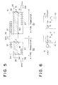
- Fig. 6 is a diagram showing an oscillation circuit known heretofore which is used in a charge pump for internally generating voltage signals to be supplied to UART (Universal Asynchronous Receiver/Transmitter), EEPROM (Electrically Erasable and Programmable Read-Only Memory) and others incorporated in microcomputers, IC cards and others.
- the oscillation circuit includes a NAND circuit 1 having first and second input terminals, a first inverter 2 having an input terminal to which the output terminal of the NAND circuit 1 is connected and an output terminal connected to one end of a first capacitor 4 via a first resistor 3. The other end of the first capacitor 4 is grounded.
- a junction (i.e., node of connection) between the first resistor 3 and the first capacitor 4 is connected to an input terminal of a second inverter 5 which has an output terminal connected to one end of a second capacitor 7 via a second resistor 6. The other end of the second capacitor 7 is grounded.
- a junction between the second resistor 6 and the second capacitor 7 is connected to an output terminal 8 of the oscillation circuit on one hand and connected to the second input terminal of the NAND circuit 1 on the other hand.
- the first input terminal of the NAND circuit 1 is connected to an input terminal 9 of the oscillation circuit.
- the first inverter 2, the first resistor 3 and the first capacitor 4 constitute one circuit unit 10a
- the another circuit unit 10b is constituted by the second inverter 5, the second resistor 6 and the second capacitor 7.
- more than two circuit units of the same configuration as the circuit units 10a and 10b may be connected in cascade, if desired.
- an enable signal EN is supplied to the first input terminal of the NAND circuit 1 from a CPU (Central Processing Unit) or the like incorporated in the microcomputer or IC card.
- the enable signal EN is fixed to a low level (L)
- the output of the NAND circuit 1 assumes a high level (H).
- This high-level output of the NAND circuit 1 is transmitted to the output terminal 8 via a series connection of the first inverter 2 and the first resistor 3 as well as the second inverter 5 and the second resistor 6 connected in series.
- an output signal OUT of high level (H) appears at the output terminal 8 of the oscillation circuit.
- This output signal OUT is fed back to the second input terminal of the NAND circuit 1.
- the enable signal EN applied to the first input terminal of the NAND circuit 1 is fixed at the low level, the output of the NAND circuit 1 remains constantly at the high level.
- the output of the NAND circuit 1 changes from the high to the low level, which results in change of the output signal OUT at the output terminal 8 to the low level from the high level.
- the feedback signal applied to the second input terminal of the NAND circuit 1 becomes low. Consequently, the output of the NAND circuit 1 becomes high with the result that the level of the output signal OUT at the output terminal 8 is also high.
- the waveform 7 shows a waveform of the oscillation signal outputted from the output terminal 8.
- the curvilinear rising edges and falling edges of the pulse-like waves are determined in dependence on the time constant mentioned above.
- the signal will have to be shaped by a suitable shaper circuit.
- each of the circuit units 10a and 10b includes a single inverter (2 or 5), the oscillation frequency characteristics of the oscillation circuit depend on the driving capability of the first inverter 2 or the second inverter 5 to a great extent.
- driving capability used herein, it is contemplated to mean a parameter indicating magnitude of a current which can be driven by the inverter. Since the inverter is constituted by an N-channel transistor and a P-channel transistor, the driving capability of the former is determined by that of the latter.
- the frequency of oscillation depends on a time constant (a delay factor) which in turn is determined by values of the resistor (3, 6) and the capacitor (4, 7) connected to the inverter (2, 5).
- the transistor itself which constitutes the inverter (2, 5) has a resistance component (internal resistance) which bears such relation to the driving capability of the inverter (2, 5) that the internal resistance assumes a smaller value as the driving capability becomes greater and vice versa.
- the influence of the internal resistance of the transistors constituting the inverter becomes significant to make dull the waveform of the output signal of the oscillation circuit (i.e., the time taken for the rising and falling of the pulse is increased), which results in that the oscillation frequency deviates from a preset value to a lower frequency.
- the driving capability of the inverters 2 and 5 are enhanced, the influence to dullness of the waveform (and hence deviation from the preset frequency) can certainly be mitigated.
- power consumption of the inverters and hence the oscillation circuit increases, giving rise to a problem.
- prior art document US-A-5 030 853 discloses logic and memory circuits optimized with respect to speed and density.
- inverters in a ring oscillator are designed such that each of a plurality of inverter stages has a symmetric voltage transfer function.
- a further conventionally known oscillation circuit is disclosed in document US-A-5 180 995, comprising inversion circuits and RC delay elements in a ring.
- This prior art document teaches the compensation of oscillation frequency variations which are due to a change, namely, a rise of the ambient temperature as an externally influencing parameter.
- the compensation is achieved by a specific temperature characteristic of a resistor provided within the circuit arrangement.
- the power consumption can effectively be prevented from increasing because magnitude of a through-current can be decreased by lowering the driving capability of the first stage inverter for which the input signal has a waveform dulled. Further, by enhancing the driving capability of the final stage inverter for which the input signal rises up and falls sharply, influence of the internal resistance to the time constant can be suppressed to a minimum, whereby the oscillation frequency can be prevented from variation or fluctuation.
- an oscillation circuit which can operate stably over a wide range of voltages.
- the second inversion circuit mentioned above may include at least one intermediate stage inverter connected between the first stage inverter and the final stage inverter, wherein driving capability of the intermediate stage inverter is made higher than that of the first stage inverter and lower than that of the final stage inverter.
- the second inversion circuit previously mentioned may include a plurality of intermediate stage inverters connected in series between the first stage inverter and the final stage inverter, wherein driving capabilities of the plurality of intermediate stage inverters are progressively and sequentially increased, starting from the one connected immediately after the first stage inverter toward the final stage inverter.
- Fig. 1 is a circuit diagram showing a configuration of an oscillation circuit according to an embodiment of the present invention which is adapted to be incorporated in microcomputers, IC cards or the like.
- a NAND circuit 11 has two input terminals, a first terminal of which is connected to an input terminal 23 of the oscillation circuit.
- a trigger signal generated by a CPU (Central Processing Unit) incorporated in a microcomputer, an IC card or the like is inputted to the input terminal 23 as an enable signal EN for triggering operation of the oscillation circuit.
- the NAND circuit 11 has an output terminal connected to an input terminal of a first delay circuit D1 via a first inverter 12 which serves as a first inversion circuit.
- the output terminal of the first delay circuit D1 is connected to an input terminal of a second inversion circuit IV of which output terminal is connected to an input terminal of a second delay circuit D2.
- the first delay circuit D1 includes a first resistor 13 having one end connected to the output terminal of the first inverter 12 and a first capacitor 14 having one end connected to the other end of the first resistor 13. The other end of the capacitor 14 is grounded. A junction (i.e., connecting node or point) between the first resistor 13 and the first capacitor 14 is connected to the input terminal of the second inversion circuit IV.
- the second inversion circuit IV includes a second inverter 15 constituting a first stage inverter, a third inverter 16 constituting an intermediate stage inverter and a fourth inverter 17 serving as a final stage inverter, wherein the input terminal of the second inverter 15 is connected to the junction between the first resistor 13 and the first capacitor 14.
- the second delay circuit D2 includes a second resistor 18 having one end connected to the output terminal of the fourth inverter 17 and a second capacitor 19 having one end connected to the other end of the second resistor 18.
- the other end of the capacitor 19 is connected to the ground.
- a junction between the second resistor 18 and the second capacitor 19 is connected to the output terminal 20 of the oscillation circuit for generating an output signal which can be utilized as a clock signal for a UART (Universal Asynchronous Receiver/Transmitter), an EEPROM (Electrically Erasable and Programmable Read-Only Memory) and others incorporated in the microcomputer, IC card or the like.
- the junction between the second resistor 18 and the second capacitor 19 is connected to a second input terminal of the NAND circuit 11 via fifth and sixth inverters 21 and 22 connected in series.
- Fig. 2 is a waveform diagram showing a waveform of a signal supplied to the first-stage inverter 15
- Fig. 3 is a waveform diagram showing a waveform of an output signal output from the final-stage inverter 17.
- Fig. 4 is a circuit diagram showing a typical structure of the inverter 15, 16 or 17 shown in Fig. 1.
- the inverter is realized in the form of a CMOS (Complementary Metal-Oxide Semiconductor) device in which a P-type transistor 51 and an N-type transistor 52 are connected in a complementary manner. More specifically, the P-type transistor 51 and the N-type transistor 52 have respective gates which are interconnected so as to form an input terminal (IN).
- the P-type transistor 51 has a source connected to a power source 55, while the N-type transistor 52 has a source connected to the ground potential.
- the drain of the P-type transistor 51 and the drain of the N-type transistor 52 are connected together to form an output terminal (OUT).
- a through-current (which may also be referred to as the rush current) flows from the power source 52 to the ground 56 (i.e., in the direction indicated by an arrow 57) via the P-type transistor 51 and the N-type transistor 52.
- the P-type transistor 51 is first turned on and then the N-type transistor 52 is turned off. Consequently, during a period in which the input signal falls from the high level to the low level, both of the P-type transistor 51 and the N-type transistor 52 are temporarily set to the conducting state to allow the through-current to flow from the power source 55 to the ground 56.
- Fig. 5 is a diagram for illustrating a physical structure or layout arrangement of the inverter shown in Fig. 4.
- the P-type transistor 51 has a field region 31, a gate region 32 and a signal input region 33.
- the N-type transistor 52 has a field region 34 and a gate region 35.
- Aluminum wires 36, 38 and 39 are connected to the output terminal, the ground and the power source, respectively.
- Contact regions 37 are provided for making electrical contacts between the aluminum wires 36, 38 and 39 and the field regions 31 and 32, respectively.
- the input signal for the second inverter 15 disposed at the input side of the second inversion circuit IV and constituting the so-called first stage inverter is caused to flow through the first delay circuit D1 constituted by the first resistor 13 and the first capacitor 14 before being inputted to the second inverter 15 and thus dulled in the waveform, as illustrated in Fig. 2. Consequently, if the driving capability of the second inverter 15 is enhanced, the period during which both the P-type transistor 51 and the N-type transistor 52 of the second inverter 15 are simultaneously in the conducting state is elongated, as a result of which the temporal period during which the through-current flows from the power source 55 to the ground 51 is extended, thus involving increase in the power consumption.
- the waveform of the signal inputted to the fourth inverter 17 corresponding to the final stage inverter provided at the output side can evade from becoming dull (i.e., this pulse signal has sharp or steep rising edge and falling edge). Accordingly, increase or enhancement of the driving capability of the fourth inverter 17 is not accompanied with any appreciable increase in the duration of the through-current and hence in the power consumption.
- the driving capability of each of the inverters 15 to 17 is determined by the driving capabilities of the P-type transistor 51 and the N-type transistor 52 which constitute the inverter.
- P represents a constant determined by various parameters (temperature, manufacturing process, material, impurity concentration, thickness of gate oxide film, dielectric constant, etc.) in the semiconductor manufacturing processes
- L represents a length of the gate of the transistor
- W represents a width of the same.
- the driving capability of the inverter constituted by the P-type transistor 51 and the N-type transistor 52 as shown in Fig. 5 increases as the lengths L1 and L2 of the gates of the P-type transistor 51 and the N-type transistor 52, respectively, is dimensioned shorter and/or as the widths W1 and W2 of the N-type transistor 52 and the P-type transistor 51, respectively, is dimensioned greater.
- magnitude of the current flowing through the transistors 51 and 52 increases as the input voltage is higher and vice versa.
- the driving capabilities of the transistors 51 and 52 are increased (with the internal resistance being decreased) and vice versa.
- the output frequency rate of the second delay circuit D2 becomes low.
- the driving capability of the second inverter 15 constituting the first stage inverter disposed at the input side of the second inversion circuit IV is reduced because it is sufficient for the second inverter 15 to drive only the third inverter 16, while the driving capability of the fourth inverter 17 constituting the final stage inverter is increased, whereby the influence of the internal resistance which affects the time constant of the oscillation circuit is suppressed to a possible minimum.
- deviation of the oscillation frequency from the preset frequency can effectively be avoided even when the overall driving capability of the second inversion circuit IV is set to be low, while the power consumption can profitably be prevented from increasing even when the overall driving capability of the second inversion circuit IV is set to be high. In this manner, there can be ensured highly stable operation of the oscillation circuit over a wide voltage range from about 2.7 volts to about 5.5 volts while decreasing effectively the power consumption.
- the fourth inverter 17 of the final stage may fail to drive the current satisfactorily, which may eventually lead to no occurrence of oscillation.
- Such unwanted situation can be evaded by providing the third inverter 16 as the intermediate stage inverter and selecting the driving capability of the third inverter 16 higher than the second inverter 15 and lower than the fourth inverter 17.
- the number of the intermediate stage inverters may be increased, as occasion requires. In that case, however, the number of the inverter elements (inclusive of the NAND circuit) in the oscillation circuit as a whole should be selected to be an odd number, because, if otherwise, no oscillation can take place.
- the second inversion circuit IV is constituted by a plurality of inverters 15 to 17. It is, however, to be noted that the first inversion circuit 12 may equally be constituted by a plurality of inverters. Further, the second inversion circuit IV and the second delay circuit D2 may be provided in pluralities, respectively.
- the oscillation circuit according to the invention is never limited to any particular utilization but may find a great variety of applications covering not only the existing microcomputers and IC cards but also those which will be developed in the future. Accordingly, the terms "microcomputer”, “IC card” or “computer system” used herein should be interpreted in their broadest sense. Thus, it should be understood that all suitable modifications may be resorted to.
Landscapes
- Pulse Circuits (AREA)
- Logic Circuits (AREA)
- Electronic Switches (AREA)
- Semiconductor Integrated Circuits (AREA)
Claims (6)
- Oszillatorschaltung mitdadurch gekennzeichnet, daßeiner Vielzahl von Invertierungsschaltungen (12, IV) und einer Vielzahl von Verzögerungsschaltungen (D1, D2), wobei jede Verzögerungsschaltungen (D1, D2) ein RC-Element umfaßt,wobei zumindest eine der Invertierungsschaltungen (IV) durch eine Vielzahl von zueinander in Reihe geschalteten Invertierern (15, 16, 17) gebildet ist,die Ansteuerfähigkeit einer ersten Invertiererstufe (15) der vielen Invertierer, die unmittelbar nach der bei der Eingangsseite der Oszillatorschaltung ausgestalteten Verzögerungsschaltung (D1) eingefügt ist, kleiner gemacht wird als die Ansteuerfähigkeit einer letzten Invertiererstufe (17), die unmittelbar vor der bei der Ausgangsseite der Oszillatorschaltung ausgestalteten Verzögerungsschaltung (D2) eingefügt ist,wobei die Ansteuerfähigkeit der Invertierer in Abhängigkeit des Verhältnisses (W/L) zwischen der Breite (W) und der Länge (L) des Gate-Bereichs der jeweils einen der Invertierer bildenden Transistoren bestimmt ist,und wobei keine weitere Verzögerungsschaltung im Signalweg zwischen den Verzögerungsschaltungen (D1, D2) angeschlossen ist.
- Oszillatorschaltung nach Anspruch 1, zusätzlich mitwobeieiner NAND-Schaltung (11) miteinem ersten Eingangsanschluß, dem ein extern zugeführtes Triggersignal (EN) zugeführt wird,einem zweiten Eingangsanschluß undeinem Ausgangsanschluß,der Ausgangsanschluß der NAND-Schaltung mit einer ersten Invertierungsschaltung (12) der Vielzahl von Invertierungsschaltungen der Oszillatorschaltung verbunden ist,der Ausgangsanschluß der Invertierungsschaltung (12) mit einer ersten Verzögerungsschaltung (D1) der Vielzahl von integrierenden Verzögerungsschaltungen verbunden ist, die bei der Eingangsseite der Oszillatorschaltung ausgestaltet sind, undder Ausgangsanschluß der zweiten Verzögerungsschaltung (D2) der Vielzahl von integrierenden Verzögerungsschaltungen zu dem zweiten Eingangsanschluß der NAND-Schaltung zurückgeführt wird.
- Oszillatorschaltung nach Anspruch 2,wobei die zumindest eine zweite Invertierungsschaltung (IV) zumindest eine Zwischeninvertiererstufe (16) aufweist, die zwischen der ersten Invertiererstufe (15) und der letzten Invertiererstufe (17) angeschlossen ist,wobei die Ansteuerfähigkeit der Zwischeninvertiererstufe (16) größer ist als die der ersten Invertiererstufe (15) und kleiner ist als die der letzten Invertiererstufe (17).
- Oszillatorschaltung nach Anspruch 3,wobei die zumindest eine zweite Invertierungsschaltung (IV) eine Vielzahl von Zwischeninvertiererstufen aufweist, die in Reihe zwischen der ersten Invertiererstufe (15) und der letzten Invertiererstufe (17) geschaltet sind,wobei die Ansteuerfähigkeiten der Vielzahl von Zwischeninvertiererstufen stufenweise und aufeinanderfolgend vergrößert werden, angefangen bei der unmittelbar nach der ersten Invertiererstufe (15) angeschlossenen Zwischeninvertiererstufe bis zu letzten Invertiererstufe (17).
- Oszillatorschaltung nach Anspruch 1 oder 2 zur Verwendung als Taktsignalerzeugungseinrichtung in einem Computersystem, wobei das Computersystem intern ein Signal zur Triggerung des Betriebs der Oszillatorschaltung erzeugt.
- Oszillatorschaltung nach Anspruch 1 oder 2 zur Verwendung als Taktsignalerzeugungseinrichtung in einer IC-Karten-Vorrichtung.
Applications Claiming Priority (2)
| Application Number | Priority Date | Filing Date | Title |
|---|---|---|---|
| JP5175323A JPH0730378A (ja) | 1993-07-15 | 1993-07-15 | 発振回路 |
| JP175323/93 | 1993-07-15 |
Publications (3)
| Publication Number | Publication Date |
|---|---|
| EP0634837A2 EP0634837A2 (de) | 1995-01-18 |
| EP0634837A3 EP0634837A3 (de) | 1995-08-30 |
| EP0634837B1 true EP0634837B1 (de) | 1999-02-17 |
Family
ID=15994076
Family Applications (1)
| Application Number | Title | Priority Date | Filing Date |
|---|---|---|---|
| EP94110885A Expired - Lifetime EP0634837B1 (de) | 1993-07-15 | 1994-07-13 | Oszillatorschaltung, auch in Mikrorechnern und in Chipkarten verwendet |
Country Status (4)
| Country | Link |
|---|---|
| US (1) | US5424690A (de) |
| EP (1) | EP0634837B1 (de) |
| JP (1) | JPH0730378A (de) |
| DE (1) | DE69416549T2 (de) |
Families Citing this family (16)
| Publication number | Priority date | Publication date | Assignee | Title |
|---|---|---|---|---|
| JP3140623B2 (ja) * | 1993-12-20 | 2001-03-05 | 富士通株式会社 | 発振回路装置 |
| CN1107922C (zh) * | 1995-06-16 | 2003-05-07 | 罗姆股份有限公司 | 半导体器件,使用同样器件的ic卡和通信系统 |
| DE69531349D1 (de) * | 1995-10-31 | 2003-08-28 | St Microelectronics Srl | Spannungsgenerator für nichtflüchtige elektrisch-programmierbare Speicherzellen |
| US6052013A (en) * | 1998-04-21 | 2000-04-18 | Vanguard International Semiconductor Corporation | Apparatus for generating a timing signal |
| KR100354904B1 (ko) * | 1998-05-19 | 2002-12-26 | 삼성전자 주식회사 | 광시야각액정표시장치 |
| TW483251B (en) * | 2000-11-23 | 2002-04-11 | Macronix Int Co Ltd | Clock generator with stable frequency |
| KR100353544B1 (en) * | 2000-12-27 | 2002-09-27 | Hynix Semiconductor Inc | Circuit for generating internal supply voltage of semiconductor memory device |
| US6952117B2 (en) * | 2002-03-08 | 2005-10-04 | Micron Technology Inc. | Distributed clock generator for semiconductor devices and related method of operating semiconductor devices |
| US6888406B2 (en) * | 2002-08-12 | 2005-05-03 | Microtune (Texas), L.P. | Highly linear variable gain amplifier |
| US6809960B2 (en) | 2002-08-26 | 2004-10-26 | Micron Technology, Inc. | High speed low voltage driver |
| JP2004096237A (ja) * | 2002-08-29 | 2004-03-25 | Nec Electronics Corp | 発振回路及び半導体集積回路 |
| RU2237352C1 (ru) * | 2003-03-03 | 2004-09-27 | Российский Федеральный Ядерный Центр - Всероссийский Научно-Исследовательский Институт Экспериментальной Физики | Мультивибратор |
| US7667549B2 (en) * | 2007-04-26 | 2010-02-23 | Semiconductor Energy Laboratory Co., Ltd. | Semiconductor device and driving method thereof |
| KR100983771B1 (ko) | 2008-05-19 | 2010-09-27 | 덴소풍성전자(주) | 저 전압용 링 발진기 |
| KR101679430B1 (ko) * | 2010-09-30 | 2016-11-25 | 삼성전자주식회사 | 휴대단말기에서 심카드의 삽입을 인식하는 방법 및 장치 |
| GB2583353B (en) | 2019-04-24 | 2023-04-12 | Pragmatic Printing Ltd | An oscillator with improved frequency stability |
Citations (1)
| Publication number | Priority date | Publication date | Assignee | Title |
|---|---|---|---|---|
| US5191232A (en) * | 1992-03-17 | 1993-03-02 | Silicon Storage Technology, Inc. | High frequency voltage multiplier for an electrically erasable and programmable memory device |
Family Cites Families (8)
| Publication number | Priority date | Publication date | Assignee | Title |
|---|---|---|---|---|
| US4536720A (en) * | 1983-11-14 | 1985-08-20 | International Business Machines Corporation | Programmable oscillator with power down feature and frequency adjustment |
| DE3401610A1 (de) * | 1984-01-18 | 1985-07-18 | Siemens AG, 1000 Berlin und 8000 München | Integrierte halbleiterschaltung mit einem ringoszillator |
| JPS6143814A (ja) * | 1984-08-07 | 1986-03-03 | Mitsubishi Electric Corp | 発振回路 |
| US5030853A (en) * | 1990-03-21 | 1991-07-09 | Thunderbird Technologies, Inc. | High speed logic and memory family using ring segment buffer |
| JP2557271B2 (ja) * | 1990-04-06 | 1996-11-27 | 三菱電機株式会社 | 内部降圧電源電圧を有する半導体装置における基板電圧発生回路 |
| JPH04172711A (ja) * | 1990-11-06 | 1992-06-19 | Mitsubishi Electric Corp | 半導体遅延回路 |
| US5081428A (en) * | 1991-03-29 | 1992-01-14 | Codex Corp. | Voltage controlled oscillator having 50% duty cycle clock |
| JPH06169237A (ja) * | 1991-09-13 | 1994-06-14 | Mitsubishi Electric Corp | リングオシレータ回路 |
-
1993
- 1993-07-15 JP JP5175323A patent/JPH0730378A/ja active Pending
-
1994
- 1994-07-06 US US08/268,115 patent/US5424690A/en not_active Expired - Fee Related
- 1994-07-13 EP EP94110885A patent/EP0634837B1/de not_active Expired - Lifetime
- 1994-07-13 DE DE69416549T patent/DE69416549T2/de not_active Expired - Fee Related
Patent Citations (1)
| Publication number | Priority date | Publication date | Assignee | Title |
|---|---|---|---|---|
| US5191232A (en) * | 1992-03-17 | 1993-03-02 | Silicon Storage Technology, Inc. | High frequency voltage multiplier for an electrically erasable and programmable memory device |
Non-Patent Citations (1)
| Title |
|---|
| L.A.GLASSER et al., "The Design and Analysis of VLSI Circuits", Addison-Wesley Publishing Company, Reading, Massachusetts, US, pages 6-11 and 253-259 * |
Also Published As
| Publication number | Publication date |
|---|---|
| DE69416549T2 (de) | 1999-08-12 |
| US5424690A (en) | 1995-06-13 |
| EP0634837A3 (de) | 1995-08-30 |
| DE69416549D1 (de) | 1999-03-25 |
| EP0634837A2 (de) | 1995-01-18 |
| JPH0730378A (ja) | 1995-01-31 |
Similar Documents
| Publication | Publication Date | Title |
|---|---|---|
| EP0634837B1 (de) | Oszillatorschaltung, auch in Mikrorechnern und in Chipkarten verwendet | |
| US4779013A (en) | Slew-rate limited output driver having reduced switching noise | |
| US4617529A (en) | Ring oscillator with delay element and potential pulling circuit | |
| US4996443A (en) | Integrated circuit for level shift | |
| EP0410473B1 (de) | Integrierte Halbleiterschaltung | |
| US5041741A (en) | Transient immune input buffer | |
| EP0952668A2 (de) | Stabile Ausgangspufferschaltung bei niedriger Anstiegsgeschwindigkeit | |
| JPH11177398A (ja) | 遅延回路 | |
| EP0129580A1 (de) | Taktimpulsformerschaltung | |
| US6670841B2 (en) | Level shifting circuit | |
| EP0735688A2 (de) | Adiabatische Logik | |
| US5705946A (en) | Low power low voltage level shifter | |
| EP0350879B1 (de) | Ausgangstreiberschaltung für Halbleiter-IC | |
| EP0549378B1 (de) | Einschalt-Rücksetzschaltung | |
| US4216389A (en) | Bus driver/latch with second stage stack input | |
| US4352996A (en) | IGFET Clock generator circuit employing MOS boatstrap capacitive drive | |
| US6346835B1 (en) | Power-on reset signal preparing circuit | |
| EP0735683A2 (de) | Logikgatterschaltung und digitale integrierte Schaltung | |
| US6867629B2 (en) | Integrated circuit and method of adjusting capacitance of a node of an integrated circuit | |
| US4837463A (en) | Three-state complementary field effect integrated circuit | |
| US5982247A (en) | CR oscillating circuit | |
| KR100313512B1 (ko) | 파워 온 검출회로 | |
| EP0735453B1 (de) | Verzögerungsschaltung und Verfahren | |
| KR960001858B1 (ko) | 반도체 메모리 장치의 데이타 출력 구동 회로 | |
| JP2574839B2 (ja) | クロック駆動回路 |
Legal Events
| Date | Code | Title | Description |
|---|---|---|---|
| PUAI | Public reference made under article 153(3) epc to a published international application that has entered the european phase |
Free format text: ORIGINAL CODE: 0009012 |
|
| AK | Designated contracting states |
Kind code of ref document: A2 Designated state(s): DE FR GB |
|
| PUAL | Search report despatched |
Free format text: ORIGINAL CODE: 0009013 |
|
| AK | Designated contracting states |
Kind code of ref document: A3 Designated state(s): DE FR GB |
|
| 17P | Request for examination filed |
Effective date: 19960102 |
|
| 17Q | First examination report despatched |
Effective date: 19961028 |
|
| GRAG | Despatch of communication of intention to grant |
Free format text: ORIGINAL CODE: EPIDOS AGRA |
|
| GRAG | Despatch of communication of intention to grant |
Free format text: ORIGINAL CODE: EPIDOS AGRA |
|
| GRAH | Despatch of communication of intention to grant a patent |
Free format text: ORIGINAL CODE: EPIDOS IGRA |
|
| GRAH | Despatch of communication of intention to grant a patent |
Free format text: ORIGINAL CODE: EPIDOS IGRA |
|
| GRAA | (expected) grant |
Free format text: ORIGINAL CODE: 0009210 |
|
| AK | Designated contracting states |
Kind code of ref document: B1 Designated state(s): DE FR GB |
|
| REF | Corresponds to: |
Ref document number: 69416549 Country of ref document: DE Date of ref document: 19990325 |
|
| ET | Fr: translation filed | ||
| PLBE | No opposition filed within time limit |
Free format text: ORIGINAL CODE: 0009261 |
|
| STAA | Information on the status of an ep patent application or granted ep patent |
Free format text: STATUS: NO OPPOSITION FILED WITHIN TIME LIMIT |
|
| 26N | No opposition filed | ||
| PGFP | Annual fee paid to national office [announced via postgrant information from national office to epo] |
Ref country code: DE Payment date: 20010709 Year of fee payment: 8 |
|
| PGFP | Annual fee paid to national office [announced via postgrant information from national office to epo] |
Ref country code: GB Payment date: 20010711 Year of fee payment: 8 |
|
| PGFP | Annual fee paid to national office [announced via postgrant information from national office to epo] |
Ref country code: FR Payment date: 20010712 Year of fee payment: 8 |
|
| REG | Reference to a national code |
Ref country code: GB Ref legal event code: IF02 |
|
| PG25 | Lapsed in a contracting state [announced via postgrant information from national office to epo] |
Ref country code: GB Free format text: LAPSE BECAUSE OF NON-PAYMENT OF DUE FEES Effective date: 20020713 |
|
| PG25 | Lapsed in a contracting state [announced via postgrant information from national office to epo] |
Ref country code: DE Free format text: LAPSE BECAUSE OF NON-PAYMENT OF DUE FEES Effective date: 20030201 |
|
| GBPC | Gb: european patent ceased through non-payment of renewal fee |
Effective date: 20020713 |
|
| PG25 | Lapsed in a contracting state [announced via postgrant information from national office to epo] |
Ref country code: FR Free format text: LAPSE BECAUSE OF NON-PAYMENT OF DUE FEES Effective date: 20030331 |
|
| REG | Reference to a national code |
Ref country code: FR Ref legal event code: ST |