EP0629007B1 - Piezoelectric device - Google Patents
Piezoelectric device Download PDFInfo
- Publication number
- EP0629007B1 EP0629007B1 EP94304112A EP94304112A EP0629007B1 EP 0629007 B1 EP0629007 B1 EP 0629007B1 EP 94304112 A EP94304112 A EP 94304112A EP 94304112 A EP94304112 A EP 94304112A EP 0629007 B1 EP0629007 B1 EP 0629007B1
- Authority
- EP
- European Patent Office
- Prior art keywords
- layer
- piezoelectric
- substrate
- cavity
- piezoelectric device
- Prior art date
- Legal status (The legal status is an assumption and is not a legal conclusion. Google has not performed a legal analysis and makes no representation as to the accuracy of the status listed.)
- Expired - Lifetime
Links
- 239000000758 substrate Substances 0.000 claims description 159
- 239000000463 material Substances 0.000 claims description 53
- 238000006073 displacement reaction Methods 0.000 claims description 41
- 239000000919 ceramic Substances 0.000 claims description 36
- 230000002093 peripheral effect Effects 0.000 claims description 20
- 239000000203 mixture Substances 0.000 claims description 19
- 230000008859 change Effects 0.000 claims description 8
- 239000013078 crystal Substances 0.000 claims description 8
- NKZSPGSOXYXWQA-UHFFFAOYSA-N dioxido(oxo)titanium;lead(2+) Chemical compound [Pb+2].[O-][Ti]([O-])=O NKZSPGSOXYXWQA-UHFFFAOYSA-N 0.000 claims description 8
- ZBSCCQXBYNSKPV-UHFFFAOYSA-N oxolead;oxomagnesium;2,4,5-trioxa-1$l^{5},3$l^{5}-diniobabicyclo[1.1.1]pentane 1,3-dioxide Chemical compound [Mg]=O.[Pb]=O.[Pb]=O.[Pb]=O.O1[Nb]2(=O)O[Nb]1(=O)O2 ZBSCCQXBYNSKPV-UHFFFAOYSA-N 0.000 claims description 8
- RVTZCBVAJQQJTK-UHFFFAOYSA-N oxygen(2-);zirconium(4+) Chemical compound [O-2].[O-2].[Zr+4] RVTZCBVAJQQJTK-UHFFFAOYSA-N 0.000 claims description 8
- 229910001928 zirconium oxide Inorganic materials 0.000 claims description 8
- HFGPZNIAWCZYJU-UHFFFAOYSA-N lead zirconate titanate Chemical compound [O-2].[O-2].[O-2].[O-2].[O-2].[Ti+4].[Zr+4].[Pb+2] HFGPZNIAWCZYJU-UHFFFAOYSA-N 0.000 claims description 7
- SIWVEOZUMHYXCS-UHFFFAOYSA-N oxo(oxoyttriooxy)yttrium Chemical compound O=[Y]O[Y]=O SIWVEOZUMHYXCS-UHFFFAOYSA-N 0.000 claims description 5
- BRPQOXSCLDDYGP-UHFFFAOYSA-N calcium oxide Chemical compound [O-2].[Ca+2] BRPQOXSCLDDYGP-UHFFFAOYSA-N 0.000 claims description 3
- 239000000292 calcium oxide Substances 0.000 claims description 3
- ODINCKMPIJJUCX-UHFFFAOYSA-N calcium oxide Inorganic materials [Ca]=O ODINCKMPIJJUCX-UHFFFAOYSA-N 0.000 claims description 3
- 229910000420 cerium oxide Inorganic materials 0.000 claims description 3
- HEPLMSKRHVKCAQ-UHFFFAOYSA-N lead nickel Chemical compound [Ni].[Pb] HEPLMSKRHVKCAQ-UHFFFAOYSA-N 0.000 claims description 3
- 239000000395 magnesium oxide Substances 0.000 claims description 3
- CPLXHLVBOLITMK-UHFFFAOYSA-N magnesium oxide Inorganic materials [Mg]=O CPLXHLVBOLITMK-UHFFFAOYSA-N 0.000 claims description 3
- AXZKOIWUVFPNLO-UHFFFAOYSA-N magnesium;oxygen(2-) Chemical compound [O-2].[Mg+2] AXZKOIWUVFPNLO-UHFFFAOYSA-N 0.000 claims description 3
- BMMGVYCKOGBVEV-UHFFFAOYSA-N oxo(oxoceriooxy)cerium Chemical compound [Ce]=O.O=[Ce]=O BMMGVYCKOGBVEV-UHFFFAOYSA-N 0.000 claims description 3
- 238000000034 method Methods 0.000 description 30
- 230000015572 biosynthetic process Effects 0.000 description 22
- 239000010408 film Substances 0.000 description 22
- 230000008569 process Effects 0.000 description 22
- 238000010304 firing Methods 0.000 description 13
- 230000003993 interaction Effects 0.000 description 12
- 230000000052 comparative effect Effects 0.000 description 11
- 238000010438 heat treatment Methods 0.000 description 11
- 238000004519 manufacturing process Methods 0.000 description 11
- 230000035882 stress Effects 0.000 description 10
- BASFCYQUMIYNBI-UHFFFAOYSA-N platinum Chemical compound [Pt] BASFCYQUMIYNBI-UHFFFAOYSA-N 0.000 description 8
- 238000005245 sintering Methods 0.000 description 8
- 229910010293 ceramic material Inorganic materials 0.000 description 6
- 230000006870 function Effects 0.000 description 5
- 238000007641 inkjet printing Methods 0.000 description 5
- 239000007772 electrode material Substances 0.000 description 4
- 238000002474 experimental method Methods 0.000 description 4
- 229910052451 lead zirconate titanate Inorganic materials 0.000 description 4
- 238000003754 machining Methods 0.000 description 4
- 229910052697 platinum Inorganic materials 0.000 description 4
- KDLHZDBZIXYQEI-UHFFFAOYSA-N Palladium Chemical compound [Pd] KDLHZDBZIXYQEI-UHFFFAOYSA-N 0.000 description 3
- 239000000654 additive Substances 0.000 description 3
- 239000000956 alloy Substances 0.000 description 3
- 229910045601 alloy Inorganic materials 0.000 description 3
- 239000011248 coating agent Substances 0.000 description 3
- 238000000576 coating method Methods 0.000 description 3
- 239000004020 conductor Substances 0.000 description 3
- 229910052751 metal Inorganic materials 0.000 description 3
- 239000002184 metal Substances 0.000 description 3
- 238000007639 printing Methods 0.000 description 3
- 238000007650 screen-printing Methods 0.000 description 3
- 230000003746 surface roughness Effects 0.000 description 3
- XEEYBQQBJWHFJM-UHFFFAOYSA-N Iron Chemical compound [Fe] XEEYBQQBJWHFJM-UHFFFAOYSA-N 0.000 description 2
- PXHVJJICTQNCMI-UHFFFAOYSA-N Nickel Chemical compound [Ni] PXHVJJICTQNCMI-UHFFFAOYSA-N 0.000 description 2
- VYPSYNLAJGMNEJ-UHFFFAOYSA-N Silicium dioxide Chemical compound O=[Si]=O VYPSYNLAJGMNEJ-UHFFFAOYSA-N 0.000 description 2
- GWEVSGVZZGPLCZ-UHFFFAOYSA-N Titan oxide Chemical compound O=[Ti]=O GWEVSGVZZGPLCZ-UHFFFAOYSA-N 0.000 description 2
- MCMNRKCIXSYSNV-UHFFFAOYSA-N Zirconium dioxide Chemical compound O=[Zr]=O MCMNRKCIXSYSNV-UHFFFAOYSA-N 0.000 description 2
- 229910052787 antimony Inorganic materials 0.000 description 2
- 238000005452 bending Methods 0.000 description 2
- 239000011195 cermet Substances 0.000 description 2
- 238000006243 chemical reaction Methods 0.000 description 2
- 238000005229 chemical vapour deposition Methods 0.000 description 2
- 238000004891 communication Methods 0.000 description 2
- 150000001875 compounds Chemical class 0.000 description 2
- 238000007598 dipping method Methods 0.000 description 2
- 230000000694 effects Effects 0.000 description 2
- 238000009413 insulation Methods 0.000 description 2
- 230000010354 integration Effects 0.000 description 2
- 238000005259 measurement Methods 0.000 description 2
- 229910052763 palladium Inorganic materials 0.000 description 2
- 239000000843 powder Substances 0.000 description 2
- 238000004080 punching Methods 0.000 description 2
- 229920005989 resin Polymers 0.000 description 2
- 239000011347 resin Substances 0.000 description 2
- 230000004044 response Effects 0.000 description 2
- 229910052814 silicon oxide Inorganic materials 0.000 description 2
- 238000005507 spraying Methods 0.000 description 2
- 239000000126 substance Substances 0.000 description 2
- 230000001629 suppression Effects 0.000 description 2
- OYPRJOBELJOOCE-UHFFFAOYSA-N Calcium Chemical compound [Ca] OYPRJOBELJOOCE-UHFFFAOYSA-N 0.000 description 1
- 229910052684 Cerium Inorganic materials 0.000 description 1
- VYZAMTAEIAYCRO-UHFFFAOYSA-N Chromium Chemical compound [Cr] VYZAMTAEIAYCRO-UHFFFAOYSA-N 0.000 description 1
- WHXSMMKQMYFTQS-UHFFFAOYSA-N Lithium Chemical compound [Li] WHXSMMKQMYFTQS-UHFFFAOYSA-N 0.000 description 1
- PWHULOQIROXLJO-UHFFFAOYSA-N Manganese Chemical compound [Mn] PWHULOQIROXLJO-UHFFFAOYSA-N 0.000 description 1
- HCHKCACWOHOZIP-UHFFFAOYSA-N Zinc Chemical compound [Zn] HCHKCACWOHOZIP-UHFFFAOYSA-N 0.000 description 1
- IHWJXGQYRBHUIF-UHFFFAOYSA-N [Ag].[Pt] Chemical compound [Ag].[Pt] IHWJXGQYRBHUIF-UHFFFAOYSA-N 0.000 description 1
- 230000000996 additive effect Effects 0.000 description 1
- PNEYBMLMFCGWSK-UHFFFAOYSA-N aluminium oxide Inorganic materials [O-2].[O-2].[O-2].[Al+3].[Al+3] PNEYBMLMFCGWSK-UHFFFAOYSA-N 0.000 description 1
- WATWJIUSRGPENY-UHFFFAOYSA-N antimony atom Chemical compound [Sb] WATWJIUSRGPENY-UHFFFAOYSA-N 0.000 description 1
- 229910052788 barium Inorganic materials 0.000 description 1
- DSAJWYNOEDNPEQ-UHFFFAOYSA-N barium atom Chemical compound [Ba] DSAJWYNOEDNPEQ-UHFFFAOYSA-N 0.000 description 1
- 230000008901 benefit Effects 0.000 description 1
- 229910052797 bismuth Inorganic materials 0.000 description 1
- JCXGWMGPZLAOME-UHFFFAOYSA-N bismuth atom Chemical compound [Bi] JCXGWMGPZLAOME-UHFFFAOYSA-N 0.000 description 1
- 238000005422 blasting Methods 0.000 description 1
- 229910052810 boron oxide Inorganic materials 0.000 description 1
- 229910052793 cadmium Inorganic materials 0.000 description 1
- BDOSMKKIYDKNTQ-UHFFFAOYSA-N cadmium atom Chemical compound [Cd] BDOSMKKIYDKNTQ-UHFFFAOYSA-N 0.000 description 1
- 229910052791 calcium Inorganic materials 0.000 description 1
- 239000011575 calcium Substances 0.000 description 1
- ZMIGMASIKSOYAM-UHFFFAOYSA-N cerium Chemical compound [Ce][Ce][Ce][Ce][Ce][Ce][Ce][Ce][Ce][Ce][Ce][Ce][Ce][Ce][Ce][Ce][Ce][Ce][Ce][Ce][Ce][Ce][Ce][Ce][Ce][Ce][Ce][Ce][Ce][Ce][Ce][Ce][Ce][Ce][Ce][Ce][Ce][Ce] ZMIGMASIKSOYAM-UHFFFAOYSA-N 0.000 description 1
- 229910052804 chromium Inorganic materials 0.000 description 1
- 239000011651 chromium Substances 0.000 description 1
- 239000004927 clay Substances 0.000 description 1
- 229910017052 cobalt Inorganic materials 0.000 description 1
- 239000010941 cobalt Substances 0.000 description 1
- GUTLYIVDDKVIGB-UHFFFAOYSA-N cobalt atom Chemical compound [Co] GUTLYIVDDKVIGB-UHFFFAOYSA-N 0.000 description 1
- 238000010276 construction Methods 0.000 description 1
- 238000001816 cooling Methods 0.000 description 1
- RKTYLMNFRDHKIL-UHFFFAOYSA-N copper;5,10,15,20-tetraphenylporphyrin-22,24-diide Chemical compound [Cu+2].C1=CC(C(=C2C=CC([N-]2)=C(C=2C=CC=CC=2)C=2C=CC(N=2)=C(C=2C=CC=CC=2)C2=CC=C3[N-]2)C=2C=CC=CC=2)=NC1=C3C1=CC=CC=C1 RKTYLMNFRDHKIL-UHFFFAOYSA-N 0.000 description 1
- 229910052593 corundum Inorganic materials 0.000 description 1
- 230000008878 coupling Effects 0.000 description 1
- 238000010168 coupling process Methods 0.000 description 1
- 238000005859 coupling reaction Methods 0.000 description 1
- 239000002178 crystalline material Substances 0.000 description 1
- 230000007547 defect Effects 0.000 description 1
- 230000006866 deterioration Effects 0.000 description 1
- 230000002542 deteriorative effect Effects 0.000 description 1
- JKWMSGQKBLHBQQ-UHFFFAOYSA-N diboron trioxide Chemical compound O=BOB=O JKWMSGQKBLHBQQ-UHFFFAOYSA-N 0.000 description 1
- 238000009826 distribution Methods 0.000 description 1
- -1 e.g. Inorganic materials 0.000 description 1
- 238000010894 electron beam technology Methods 0.000 description 1
- 229910002112 ferroelectric ceramic material Inorganic materials 0.000 description 1
- 239000012467 final product Substances 0.000 description 1
- YBMRDBCBODYGJE-UHFFFAOYSA-N germanium oxide Inorganic materials O=[Ge]=O YBMRDBCBODYGJE-UHFFFAOYSA-N 0.000 description 1
- 230000006872 improvement Effects 0.000 description 1
- 230000001939 inductive effect Effects 0.000 description 1
- 238000011835 investigation Methods 0.000 description 1
- 238000007733 ion plating Methods 0.000 description 1
- 238000010884 ion-beam technique Methods 0.000 description 1
- 229910052742 iron Inorganic materials 0.000 description 1
- 238000010030 laminating Methods 0.000 description 1
- 238000003475 lamination Methods 0.000 description 1
- 229910052746 lanthanum Inorganic materials 0.000 description 1
- FZLIPJUXYLNCLC-UHFFFAOYSA-N lanthanum atom Chemical compound [La] FZLIPJUXYLNCLC-UHFFFAOYSA-N 0.000 description 1
- 238000003698 laser cutting Methods 0.000 description 1
- JQJCSZOEVBFDKO-UHFFFAOYSA-N lead zinc Chemical compound [Zn].[Pb] JQJCSZOEVBFDKO-UHFFFAOYSA-N 0.000 description 1
- 229910052744 lithium Inorganic materials 0.000 description 1
- 229910052748 manganese Inorganic materials 0.000 description 1
- 239000011572 manganese Substances 0.000 description 1
- WPBNNNQJVZRUHP-UHFFFAOYSA-L manganese(2+);methyl n-[[2-(methoxycarbonylcarbamothioylamino)phenyl]carbamothioyl]carbamate;n-[2-(sulfidocarbothioylamino)ethyl]carbamodithioate Chemical compound [Mn+2].[S-]C(=S)NCCNC([S-])=S.COC(=O)NC(=S)NC1=CC=CC=C1NC(=S)NC(=O)OC WPBNNNQJVZRUHP-UHFFFAOYSA-L 0.000 description 1
- 230000008018 melting Effects 0.000 description 1
- 238000002844 melting Methods 0.000 description 1
- 150000002739 metals Chemical class 0.000 description 1
- 229910052759 nickel Inorganic materials 0.000 description 1
- 229910052758 niobium Inorganic materials 0.000 description 1
- 239000010955 niobium Substances 0.000 description 1
- GUCVJGMIXFAOAE-UHFFFAOYSA-N niobium atom Chemical compound [Nb] GUCVJGMIXFAOAE-UHFFFAOYSA-N 0.000 description 1
- 229910000510 noble metal Inorganic materials 0.000 description 1
- 230000003287 optical effect Effects 0.000 description 1
- 230000001590 oxidative effect Effects 0.000 description 1
- PVADDRMAFCOOPC-UHFFFAOYSA-N oxogermanium Chemical compound [Ge]=O PVADDRMAFCOOPC-UHFFFAOYSA-N 0.000 description 1
- SWELZOZIOHGSPA-UHFFFAOYSA-N palladium silver Chemical compound [Pd].[Ag] SWELZOZIOHGSPA-UHFFFAOYSA-N 0.000 description 1
- 239000002245 particle Substances 0.000 description 1
- 229910001392 phosphorus oxide Inorganic materials 0.000 description 1
- 238000000206 photolithography Methods 0.000 description 1
- 238000007747 plating Methods 0.000 description 1
- 230000010287 polarization Effects 0.000 description 1
- 229920001296 polysiloxane Polymers 0.000 description 1
- 230000000750 progressive effect Effects 0.000 description 1
- 230000010349 pulsation Effects 0.000 description 1
- 230000009257 reactivity Effects 0.000 description 1
- 230000009467 reduction Effects 0.000 description 1
- 229910052703 rhodium Inorganic materials 0.000 description 1
- 239000010948 rhodium Substances 0.000 description 1
- MHOVAHRLVXNVSD-UHFFFAOYSA-N rhodium atom Chemical compound [Rh] MHOVAHRLVXNVSD-UHFFFAOYSA-N 0.000 description 1
- 238000005204 segregation Methods 0.000 description 1
- 239000002002 slurry Substances 0.000 description 1
- 239000006104 solid solution Substances 0.000 description 1
- 239000000243 solution Substances 0.000 description 1
- 238000004544 sputter deposition Methods 0.000 description 1
- 230000000087 stabilizing effect Effects 0.000 description 1
- 229940071182 stannate Drugs 0.000 description 1
- 229910052712 strontium Inorganic materials 0.000 description 1
- CIOAGBVUUVVLOB-UHFFFAOYSA-N strontium atom Chemical compound [Sr] CIOAGBVUUVVLOB-UHFFFAOYSA-N 0.000 description 1
- 229920003002 synthetic resin Polymers 0.000 description 1
- 239000000057 synthetic resin Substances 0.000 description 1
- XGZGDYQRJKMWNM-UHFFFAOYSA-N tantalum tungsten Chemical compound [Ta][W][Ta] XGZGDYQRJKMWNM-UHFFFAOYSA-N 0.000 description 1
- VSAISIQCTGDGPU-UHFFFAOYSA-N tetraphosphorus hexaoxide Chemical compound O1P(O2)OP3OP1OP2O3 VSAISIQCTGDGPU-UHFFFAOYSA-N 0.000 description 1
- 230000008646 thermal stress Effects 0.000 description 1
- 239000010409 thin film Substances 0.000 description 1
- 238000007740 vapor deposition Methods 0.000 description 1
- 230000008016 vaporization Effects 0.000 description 1
- 238000009834 vaporization Methods 0.000 description 1
- 229910001845 yogo sapphire Inorganic materials 0.000 description 1
- 229910052727 yttrium Inorganic materials 0.000 description 1
- VWQVUPCCIRVNHF-UHFFFAOYSA-N yttrium atom Chemical compound [Y] VWQVUPCCIRVNHF-UHFFFAOYSA-N 0.000 description 1
- 229910052725 zinc Inorganic materials 0.000 description 1
- 239000011701 zinc Substances 0.000 description 1
Images

Classifications
-
- H—ELECTRICITY
- H10—SEMICONDUCTOR DEVICES; ELECTRIC SOLID-STATE DEVICES NOT OTHERWISE PROVIDED FOR
- H10N—ELECTRIC SOLID-STATE DEVICES NOT OTHERWISE PROVIDED FOR
- H10N30/00—Piezoelectric or electrostrictive devices
- H10N30/20—Piezoelectric or electrostrictive devices with electrical input and mechanical output, e.g. functioning as actuators or vibrators
- H10N30/204—Piezoelectric or electrostrictive devices with electrical input and mechanical output, e.g. functioning as actuators or vibrators using bending displacement, e.g. unimorph, bimorph or multimorph cantilever or membrane benders
- H10N30/2047—Membrane type
-
- B—PERFORMING OPERATIONS; TRANSPORTING
- B41—PRINTING; LINING MACHINES; TYPEWRITERS; STAMPS
- B41J—TYPEWRITERS; SELECTIVE PRINTING MECHANISMS, i.e. MECHANISMS PRINTING OTHERWISE THAN FROM A FORME; CORRECTION OF TYPOGRAPHICAL ERRORS
- B41J2/00—Typewriters or selective printing mechanisms characterised by the printing or marking process for which they are designed
- B41J2/005—Typewriters or selective printing mechanisms characterised by the printing or marking process for which they are designed characterised by bringing liquid or particles selectively into contact with a printing material
- B41J2/01—Ink jet
- B41J2/135—Nozzles
- B41J2/14—Structure thereof only for on-demand ink jet heads
- B41J2/14201—Structure of print heads with piezoelectric elements
- B41J2/14233—Structure of print heads with piezoelectric elements of film type, deformed by bending and disposed on a diaphragm
-
- H—ELECTRICITY
- H10—SEMICONDUCTOR DEVICES; ELECTRIC SOLID-STATE DEVICES NOT OTHERWISE PROVIDED FOR
- H10N—ELECTRIC SOLID-STATE DEVICES NOT OTHERWISE PROVIDED FOR
- H10N30/00—Piezoelectric or electrostrictive devices
- H10N30/01—Manufacture or treatment
- H10N30/07—Forming of piezoelectric or electrostrictive parts or bodies on an electrical element or another base
- H10N30/074—Forming of piezoelectric or electrostrictive parts or bodies on an electrical element or another base by depositing piezoelectric or electrostrictive layers, e.g. aerosol or screen printing
-
- H—ELECTRICITY
- H04—ELECTRIC COMMUNICATION TECHNIQUE
- H04R—LOUDSPEAKERS, MICROPHONES, GRAMOPHONE PICK-UPS OR LIKE ACOUSTIC ELECTROMECHANICAL TRANSDUCERS; DEAF-AID SETS; PUBLIC ADDRESS SYSTEMS
- H04R17/00—Piezoelectric transducers; Electrostrictive transducers
- H04R17/04—Gramophone pick-ups using a stylus; Recorders using a stylus
- H04R17/08—Gramophone pick-ups using a stylus; Recorders using a stylus signals being recorded or played back by vibration of a stylus in two orthogonal directions simultaneously
-
- Y—GENERAL TAGGING OF NEW TECHNOLOGICAL DEVELOPMENTS; GENERAL TAGGING OF CROSS-SECTIONAL TECHNOLOGIES SPANNING OVER SEVERAL SECTIONS OF THE IPC; TECHNICAL SUBJECTS COVERED BY FORMER USPC CROSS-REFERENCE ART COLLECTIONS [XRACs] AND DIGESTS
- Y10—TECHNICAL SUBJECTS COVERED BY FORMER USPC
- Y10T—TECHNICAL SUBJECTS COVERED BY FORMER US CLASSIFICATION
- Y10T29/00—Metal working
- Y10T29/42—Piezoelectric device making
-
- Y—GENERAL TAGGING OF NEW TECHNOLOGICAL DEVELOPMENTS; GENERAL TAGGING OF CROSS-SECTIONAL TECHNOLOGIES SPANNING OVER SEVERAL SECTIONS OF THE IPC; TECHNICAL SUBJECTS COVERED BY FORMER USPC CROSS-REFERENCE ART COLLECTIONS [XRACs] AND DIGESTS
- Y10—TECHNICAL SUBJECTS COVERED BY FORMER USPC
- Y10T—TECHNICAL SUBJECTS COVERED BY FORMER US CLASSIFICATION
- Y10T29/00—Metal working
- Y10T29/49—Method of mechanical manufacture
- Y10T29/49401—Fluid pattern dispersing device making, e.g., ink jet
Definitions
- the present invention relates to a piezoelectric device for converting an input mechanical quantity into an output electrical quantity, and vice versa.
- piezoelectric devices are typically used to convert an input mechanical stress into an output electric charge (voltage) and also to convert an input electric voltage into an output mechanical distortion. In the latter case, the device is sometimes called as an electrostrictive device.
- the term "piezoelectric device” as used herein is to be interpreted in its broadest sense, as encompassing an electrostrictive device as well.
- the term “piezoelectric material” as used herein is to be interpreted in its broadest sense as encompassing an electrostrictive material as well.
- piezoelectric devices have been used for various purposes.
- actuators capable of adjusting lengths and/or positions of the optical path on a sub-micron order, or for sensors capable of detecting a fine mechanical displacement.
- piezoelectric devices There have been various proposals directed to such demands in conjunction with application of piezoelectric devices.
- unimorph- or bimorph-type piezoelectric device which undergoes bending or flexural deformation upon application of an input electrical voltage, and which can be used for ink jet printing heads, acoustic radiators (i.e., loudspeakers and the like), vibrators, etc.
- the unimorph- or bimorph-type piezoelectric device can also be used to convert a bending or flexural deformation into an electrical voltage, e.g., as a microphone or sensor.
- an electrical voltage e.g., as a microphone or sensor.
- ink jet printing heads including a unimorph- or bimorph-type piezoelectric device in view of customers' or end users' requirement for a high-quality and high-speed printing performance, it is highly desirable to realize a high density piezoelectric device having a minimized size, which operates at a low driving voltage and yet provides a satisfactory response characteristic and an operational reliability.
- the locally thin-walled substrate may be formed by laminating a relatively thick green sheet of a first ceramic layer having window-like openings therein, and a relatively thin green sheet of a second ceramic layer without such openings. After integrating the two ceramic layers by firing to form the substrate, the openings in the first ceramic layer cooperate with the second ceramic layer to define cavities having thin-walled bottom walls which are constituted by the second ceramic layer.
- the piezoelectric transducers may each include a first electrode layer, a piezoelectric layer and a second electrode layer which are sequentially laminated with each other. The piezoelectric transducers are arranged on those outer surface regions of the substrate opposite to the relevant cavities, and are integrated with the substrate by firing.
- the piezoelectric device according to the above-mentioned proposal proved to be highly advantageous in that the locally thin-walled regions of the substrate opposite to the respective piezoelectric transducers make it possible to achieve a satisfactory operation of the transducers, and further in that the remaining, relatively thick region of the substrate serves to realize a sufficient mechanical strength of the substrate as a whole.
- the substrate and the piezoelectric transducer are generally composed of materials which are different in the chemical composition and hence in the coefficient of thermal expansion.
- undesirable residual stresses tend to be caused in the piezoelectric transducer, which may deteriorate the operational characteristics of the device as a whole.
- a highly improved piezoelectric device can be realized by effectively compensating for the difference in shrinkage of the materials for the substrate and the piezoelectric transducer.
- a highly improved piezoelectric device can be realized by eliminating or suppressing undesired interaction of the neighbouring transducers.
- the present invention thus contemplates to provide a highly improved piezoelectric device on the basis of the above-mentioned recognitions.
- the piezoelectric device according to the present invention is set out in claim 1.
- the arrangement of the piezoelectric device according to the present invention features the formation of at least one groove in the relatively thick-walled region of the substrate adjacent to and surrounding the peripheral wall of the cavity. Because the groove extends along the peripheral wall of the cavity and has a depth which is greater than the thickness of the bottom wall of the cavity, it is possible to provide a higher compliance of the relatively thick-walled substrate region adjacent to the peripheral wall of the cavity, with which the thin-walled regions of the substrate can be readily deformed upon firing shrinkage during manufacture of the device.
- the transducer during manufacture of the device can be subjected to the firing shrinkage in a relatively unrestricted sense, thereby minimizing the residual stresses in the transducer and assuring a highly improved operational characteristics of the device.
- the groove in the relatively thick-walled region of the substrate can be advantageously situated between neighbouring transducers to provide a low vibration transmissibility of the substrate between adjacent transducers. This serves to effectively eliminate or suppress undesirable interaction or crosstalk between the transducers, and makes it readily possible to uniformly achieve a desired amount of displacement of the thin-walled regions of the substrate in a direction perpendicular to the general surface of the substrate.
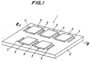
- the piezoelectric device 1 includes a locally thin-walled ceramic substrate 2 and a plurality of piezoelectric transducers 3 arranged on the upper surface of the substrate 2. More particularly, the substrate 2 has a plurality of thin-walled regions 2a and the piezoelectric transducers 3 are arranged on the thin-walled regions 2a.
- the substrate 2 has a plurality of closed cavities 4 therein, each defined by a closure wall 2b on the lower surface side of the substrate 2, peripheral walls 2c in the substrate 2 and a bottom wall on the upper surface side of the substrate 2, of which the bottom wall is constituted by the thin-walled region 2a of the substrate 2.
- the bottom wall 2a functions as a diaphragm of the piezoelectric transducer 3 in operation of the device 1.
- the substrate 2 has relatively thick-walled regions 2d adjacent to the thin-walled regions 2a, where it is formed with grooves 5 each arranged to extend along the peripheral wall 2c of the cavity 4 and to open at the upper surface of the substrate 2.
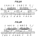
- the piezoelectric transducers 3 may be formed integrally with the substrate 2 by an ordinary film-formation process to be more fully described hereinafter, wherein a lower electrode layer 3a, a film-shaped piezoelectric layer 3b and an upper electrode layer 3c are sequentially laminated one above the other. As further shown in Figs.
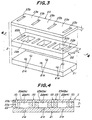
- the substrate 2 may be formed by known lamination process, wherein a lower green sheet 21 providing the closure wall 2b of the substrate 2, an intermediate green sheet 22 formed with window-like openings 22a corresponding to the cavity 4, and a thin-walled upper green sheet 23 providing the bottom wall 2a of the cavity 4, are sequentially laminated one above the other and subjected to a sintering to form an integrated substrate 2 (Fig. 4).
- the particulars of the three green sheets 21, 22, 23 forming the integrated substrate 2 will be explained below, with reference to Figs. 3 and 4.
- the upper green sheet 23 has flat regions 23a corresponding to the bottom walls 2a of the substrate 2, and slit-like openings 23b extending through the upper green sheet 23 in the direction of its thickness.
- the intermediate green sheet 22 has, besides the window-like openings 22a, slit-like grooves 22b with their bottoms situated close to the lower green sheet 21.
- the upper green sheet 23 and the intermediate green sheet 22 are superimposed with each other so that the slit-like openings 23b in the upper green sheet 23 and the slit-like grooves 22b in the intermediate green sheet 22 are brought into alignment with each other to form the groove 5 in the substrate 2.
- the lower green sheet 21 may have through-holes 21a to be used as an inlet which is in communication with an ink reservoir and/or as an outlet which is in communication with a discharge nozzle.
- the groove 5 in the substrate 2 has a length L which is at least 1/8, preferably 1/4 or more, of the length of the longitudinal edge of the cavity 4. Furthermore, as shown in Fig. 2A, the groove 5 has a depth D 1 which is substantially same as, or greater than the thickness t of the thin-walled bottom wall 2a of the cavity 4, and which preferably satisfies the following equation (1): D 1 ⁇ (t + D 2 /3) where D 2 is the depth of the cavity 4. More preferably, the depth D 1 of the groove 5 satisfies the following equation (2): D 1 ⁇ (t + 2 ⁇ D 2 /3)
- the groove 5 has a width W 1 as also shown in Fig. 2A, which is determined such that the width W 2 of the thick-walled region 2d measured between the side wall of the groove 5 and the opposite peripheral wall 2c of the cavity 4 is within a range between 20 ⁇ m and 200 ⁇ m, preferably between 20 ⁇ m and 100 ⁇ m.
- the width W 2 of the thick-walled region 2d is less than 20 ⁇ m, the stiffness of the thick-walled region 2d is often excessively lowered, making it difficult to effectively induce the desired vertical displacement of the bottom wall 2a of the cavity 4 and thereby achieve an efficient voluminal change of the cavity 4.
- the width W 2 of the thick-walled region 2d is more than 200 ⁇ m, it becomes often difficult to achieve a sufficient stress relaxation during firing of the piezoelectric film layer, and hence to effectively improve the properties of the piezoelectric material.
- due to the increased stiffness of the thick-walled region 2d it becomes difficult to achieve a sufficient lateral displacement of the peripheral wall 2c of the cavity 4 thereby to enable a large voluminal change of the cavity 4.
- width W 2 is applicable also when two or more grooves 5 are formed in each thick-walled region 2d of the substrate 2.
- the grooves 5 may have a square cross-section as shown in Figs. 2A and 4, or other appropriate cross-section such as V-shaped or trapezoid cross-section.
- the thin-walled region 2a of the substrate 2 i.e., the bottom wall of the cavity 4, which functions as the diaphragm of the piezoelectric transducer 3, in order to provide an improved high-speed response characteristic and a high conversion efficiency of the transducer 3, the thin-walled region 2a has a thickness which is preferably 50 ⁇ m or less, more preferably 30 ⁇ m or less, and further more preferably 10 ⁇ m or less.
- the piezoelectric device 1 includes groove 5 in the relatively thick-walled region 2d of the substrate 2 adjacent to and surrounding the peripheral wall 2c of the cavity 4. It is therefore possible to provide a higher compliance of the relatively thick-walled substrate region 2d adjacent to the peripheral wall 2c of the cavity 4, with which the thin-walled regions 2a of the substrate 2 can be readily deformed upon firing shrinkage during manufacture of the device 1.
- This means that the transducer 3 during manufacture of the device 1 can be subjected to the firing shrinkage in a relatively unrestricted sense, thereby minimizing the residual stresses in the transducer 3 and assuring a highly improved operational characteristics of the device 1.
- improved characteristics of the transducer 3, including the relative dielectric constant and to more fully make use of material properties which are inherent to the piezoelectric material.
- the piezoelectric device 1 when the piezoelectric device 1 according to the present invention includes an array of piezoelectric transducers 3 formed on a common substrate 2, the grooves 5 formed in the relatively thick-walled regions 2d of the substrate 2 and situated between the adjacent transducers 3 provide a low vibration transmissibility of the substrate 2 between the adjacent transducers 3.
- the grooves 5 thus serve to effectively eliminate or suppress undesirable interaction or crosstalk between adjacent transducers 3, and to make it readily possible for the thin-walled regions 2a of the substrate 2 to achieve a uniform amount of the desired vertical displacement.
- the groove 5 serves to absorb tensile forces between the transducers to thereby minimize the fluctuation in the vertical displacement amounts of the diaphragms.
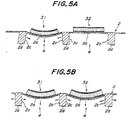
- FIGs. 5A and 5B schematically illustrate the operation of the piezoelectric device according to the above-mentioned U.S. Patent No. 5,210,455, which is provided with a plurality of piezoelectric transducers 31, 32 on a ceramic substrate 2 having open cavities 4 which are not closed by a closure wall on the lower surface side of the substrate 2.
- the present invention thus provides a unique solution for the above-mentioned problems, by forming at least one groove 5 in the thick-walled region 2d of the ceramic substrate 2.
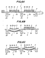
- FIGs. 6A, 6B and 6C A second embodiment of the unimorph-type piezoelectric device according to the present invention is shown in Figs. 6A, 6B and 6C, which is similar to, and directly comparable with the known device shown in Figs. 5A and 5B, in that the substrate 2 has open cavities 4. Formation of the grooves 5 in the thick-walled regions 2d of the substrate 2 makes it possible to provide a higher compliance of the diaphragm 2a and a resultant increased amount of its vertical displacement in operation of the device. As can be appreciated from Figs.
- the grooves 5 between adjacent transducers serve to effectively suppress interaction or crosstalk between the transducers, and the vertical displacement amount of the diaphragm 2a can be uniformly maintained substantially uninfluenced by the operational state of the device, i.e., regardless of whether one transducer only is actuated (Fig. 6B) or adjacent transducers are simultaneously actuated (Fig. 6C).
- FIG. 7 A third embodiment of the unimorph-type piezoelectric device according to the present invention is shown in Fig. 7, in which each thick-walled region 2d of the substrate 2 is relatively wide and formed with two grooves 5a, 5b of which the depth is greater than the thickness of the bottom wall 2a of the cavity 4.
- This embodiment effectively provides an improved compliance of the diaphragm 2a of the piezoelectric transducer 3, particularly when a plurality of transducers 3 are arranged on the substrate 2 with a relatively wide pitch.
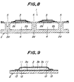
- FIG. 8 and 9 A fourth embodiment of the unimorph-type piezoelectric device according to the present invention is shown in Figs. 8 and 9, which is also provided with the grooves 5 in the thick-walled regions 2d of the substrate 2.
- This embodiment is similar to the device disclosed in the applicants' copending U.S. Patent Application No. 08/206,939 or European Patent Application No. 94 301 633.7, of which the disclosure is here incorporated by reference.
- the piezoelectric device 1 includes piezoelectric transducers 3 of which the piezoelectric layer 3b has a dimension which is sufficient to substantially completely cover the lower electrode layer 3a.
- the piezoelectric layer 3b has at least one edge 11 in the form of an extension protruding beyond the lower electrode layer 3a, which is at least locally incompletely bonded to the ceramic substrate 2, as shown at 12.
- the term 'incomplete bond refers to a specific bonded state between the ceramic substrate 2 and at least one edge 11 of the piezoelectric layer 3b, which allows the piezoelectric layer 3b to undergo a substantially unrestricted movement relative to the substrate 2.
- buffer resin layers 13 Adjacent to the edges 11 of the piezoelectric layer 3b, there may be provided buffer resin layers 13 between the upper electrode layer 3c and the substrate 2, so as to provide a smooth and flexible connection of the upper electrode layer 3c to the substrate 2 and thereby protect the upper electrode layer 3c from possible damages due to impact or vibration during the production of the device or in the use condition.
- the above-mentioned arrangement of the piezoelectric device 1 shown in Figs. 8 and 9 makes it readily possible to manufacture the piezoelectric device with an improved productivity, because it is not necessary to precisely align the edges of the piezoelectric layer 3b with those of the lower electrode layer 3a.
- the edges 11 of the piezoelectric layer 3b of the device 1 shown in Figs. 8 and 9 serve to avoid short-circuit between the lower and upper electrode layers 3a, 3c.
- the incompletely bonded regions 12 between the ceramic substrate 2 and the edge 11 of the piezoelectric layer 3b protruding beyond the lower electrode layer 3a allows the piezoelectric layer 3b to be moved relative to the substrate 2 in an unrestricted sense. It is thus possible to achieve satisfactory reliability and functions of the device, e.g., generation of large force or displacement, or of high output voltage level.
- the present invention may also be applied to a piezoelectric device which includes a single piezoelectric transducer formed on the substrate.
- formation of the grooves in the thick-walled regions of the substrate adjacent to the thin-walled bottom wall of the cavity serve to provide a higher compliance of the bottom wall and hence significantly improved operational characteristics of the device.
- the substrate 2 preferably comprises zirconium oxide as a main component, having a crystal phase that has been completely or partially stabilized preferably by the addition of at least one compound selected from a group consisting of yttrium oxide, cerium oxide, magnesium oxide and calcium oxide.
- the amount of the additives required for partially or completely stabilizing the zirconium oxide as described above may be 1-30 mol% for yttrium oxide, 6-50 mol% for cerium oxide, and 5-40 mol% for the magnesium oxide and calcium oxide.
- the amount is preferably 2-7 mol%, more preferably 2-4 mol%, because the zirconium oxide added with the yttrium oxide of such amount has a partially stabilized crystal phase and thus exhibits particularly excellent substrate characteristics.
- a preferred method of forming the ceramic substrate 2 with at least one cavity is to prepare a first green sheet having a desired thickness and at least one window-like opening formed by using a suitable mold, punching with a suitable die, or machining process, such as ultrasonic machining.
- a second, relatively thin green sheet is further prepared to have a thickness which corresponds to that of the thin-walled region of the substrate. The second green sheet is superimposed on the first green sheet under predetermined temperature/pressure condition, and then fired and integrated with each other.
- the material for the ceramic substrate 2 may contain a sintering aid, such as clay or the like.
- a sintering aid such as clay or the like.
- the cavity 4 for defining the thin-walled region 2a has a generally square contour
- the cavity 4 it is advantageous for the cavity 4 to have dimensions which are determined such that the length of the cavity is 2-20 times larger than its width.
- the transducer 3 is formed on the thin-walled region 2a of the substrate 2 over an area which preferably corresponds to 50-95% of the width of the cavity 4.
- the ceramic substrate 2 which has been formed as explained above permits satisfactory operational characteristics of the piezoelectric transducer 3 formed thereon, it is advantageous to control the surface roughness Ra of the substrate 2 to be within a range of 0.03-0.9 ⁇ m. In this instance, the distortion or stress occurring in the piezoelectric transducer 3 can be effectively transmitted to the substrate 2 having the above-mentioned range of the surface roughness Ra, and vice versa. Such a control of the surface roughness Ra is also effective to assure a high mechanical strength of the relatively thin substrate.
- the green sheet for the ceramic substrate 2 may be subjected to sintering at a temperature of 1,000°C to 1,800°C prior to formation of the piezoelectric transducer 3.
- the green sheet for the ceramic substrate 2 may be subjected to a suitable film-formation process to form the piezoelectric transducer 3 and then sintered. Formation of the piezoelectric transducer 3 on the previously sintered ceramic substrate 2 is often desirable in view of minimization of warp in the final product and dimensional accuracy of the piezoelectric transducer 3.
- the groove 5 in the thick-walled region 2d of the substrate 2 may be formed either in the green sheet before the sintering step or in the already sintered substrate, by various methods.
- the groove may be formed in the sintered substrate by an appropriate process such as laser beam process, electron beam process, slicing, blasting and ultrasonic process.
- the groove may be formed in the green sheet by press or punching with a suitable die.
- the groove formation process may be carried out either before or after the formation of the film-type piezoelectric transducer.
- the laser beam process is particularly suitable in that formation of grooves with a relatively complicated shape can be carried out in a facilitated manner.
- a suitable laser is a Nd-YAG laser having a Gaussian or normal energy distribution in the beam and using a TEM 00 single mode resonance.
- the laser beam process is performed by controlling the laser beam width to be 140 ns or less, preferably 100 ns or less, by carrying out a pulsation control by means of a Q-switch at a frequency of 3.6 kHz, for example, by concentrating the laser beam diameter to be 50 ⁇ m or less, preferably within a range of 5-10 ⁇ m, by means of an an appropriate concentration lens system, and by performing the process at a speed of 50 mm/sec or less.
- the piezoelectric transducer 3 on the ceramic substrate 2 comprising the electrode layers 3a, 3c and the piezoelectric layer 3b may be formed by a suitable film-formation process known, per se. That is to say, the film-fotmation process which may be applied to form the piezoelectric transducer 3 of the device 1 according to the present invention includes a thick-film formation process such as screen printing, spraying, dipping or coating, and a thin-film formation process such as ion beam method, sputtering, vacuum vapor deposition, ion plating, chemical vapor deposition (CVD) or plating. In particular, the thick-film formation process can be advantageously applied to form a film-like piezoelectric layer.
- a suitable film-formation process known, per se. That is to say, the film-fotmation process which may be applied to form the piezoelectric transducer 3 of the device 1 according to the present invention includes a thick-film formation process such as screen printing, spraying, dipping or coating
- the thick-film formation process makes it readily possible to form a film on the ceramic substrate by using a paste or slurry whose major component is powder of piezoelectric ceramic material.
- the powder of piezoelectric ceramic material has an average particle size within a range of 0.01 ⁇ m to 5 ⁇ m, preferably 0.05 ⁇ m to 3 ⁇ m, it is readily possible to realize excellent operational characteristics of the piezoelectric device.
- the pattern of such a film may be formed by screen printing method or photolithography method, the pattern may also be formed by removing unnecessary regions of the film by laser cutting, slicing, ultrasonic machining or other suitable machining process.
- the present invention is not limited to the specific construction, shape and/or pattern of the piezoelectric transducer illustrated in the drawings.
- the transducer may have triangular, rectangular or other polygonal shape, circular, elliptical or annular shape, comb- or lattice-like pattern, or any combination of these shapes and/or patterns.
- the electrode layers 3a, 3c and the piezoelectric layer 3b formed on the ceramic substrate 2 by a selected method as explained above may be either heat-treated in different steps for integration with the substrate each time a layer has been formed on the substrate, or simultaneously heat-treated in a single step for integration with the substrate after all the layers have been formed into a laminated structure on the substrate.
- these methods are applied to manufacture the piezoelectric device as shown in Figs. 8 and 9, it is possible to incompletely bond the edges of the piezoelectric layer 3b to the ceramic substrate 2.
- a film-formation process is used to form the electrode layers on the substrate or piezoelectric layer, it is not always a prerequisite condition to carry out the heat-treatment for integrating the film layers with the substrate or piezoelectric layer.
- the upper electrode layer 3c is preferably formed by a process which does not require heat-treatment.
- the heat treatment temperature suitable for integrating the film layers 3a, 3b, 3c of the piezoelectric transducer 3 and the ceramic substrate 2 is generally within a range of 900-1,400°C, preferably 1,000-1,400°C.
- the heat-treatment is preferably performed while controlling the atmosphere by heating the vaporization source of the piezoelectric material as well. It is also advantageous to use a method of firing the piezoelectric film layer while it is covered by a suitable cover member for preventing a direct exposure of the piezoelectric film layer to the firing atmosphere.
- the cover member consists preferably of a material which is similar to the ceramic substrate material.
- the lower and upper electrode layers 3a, 3c of the piezoelectric transducer 3 may be formed of any electrically conductive material which can withstand the oxidizing firing and the heat-treatment atmosphere at a considerably high temperature condition as explained above.
- the electrode layers may be formed of a single metal, an alloy of metals, a mixture of metal or alloy with an electrically insulating ceramic material, e.g., TiO 2 , Al 2 O 3 , ZrO 2 , etc., or an electrically conductive ceramic material.
- an electrode material whose major component is a noble metal having a high melting point, such as platinum, palladium, or rhodium, or an alloy such as silver-palladium, silver-platinum, platinum-palladium or the like. It is more preferable to use a cermet material of platinum and the ceramic material for the substrate, a cermet material of platinum and the ceramic material for the substrate and the piezoelectric material for the piezoelectric film layer, in view of an improved adhesion of the electrode layers to the piezoelectric film layer and/or the ceramic substrate. Among others, it is more preferable to use a material having a major component which comprises a platinum.
- the amount of the substrate material to be added to the electrode material is preferably 5-30% by volume, and the amount of the piezoelectric material to be added to the electrode material is preferably 5-20% by volume.
- the electrode layers 3a, 3c consisting of a conductive material as mentioned above may have a thickness of 20 ⁇ m or less, preferably 5 ⁇ m or less.
- the piezoelectric layer 3b may be formed of any piezoelectric material which exhibits a relatively large amount of field-induced strain or displacement when applied with a voltage, due to the piezoelectric effect.
- the piezoelectric material may be either a crystalline material or an amorphous material, and may be a semi-conductive material or a dielectric or ferroelectric ceramic material. Furthermore, the piezoelectric material may either require an initial polarization or poling treatment or may not require such treatment.
- the piezoelectric materials which can be used in the present invention has a composition whose major component is lead zirconate titanate (PZT), lead magnesium niobate (PMN), lead nickel niobate (PNN), lead manganese niobate, lead antimony stannate, lead zinc niobate, lead titanate, lead zirconate or a mixture or solid solution thereof.
- PZT lead zirconate titanate
- PMN lead magnesium niobate
- PNN lead nickel niobate
- lead manganese niobate lead antimony stannate
- lead zinc niobate lead titanate
- lead zirconate or a mixture or solid solution thereof.
- the piezoelectric materials indicated above whose major component is PZT or the like, may be added with a suitable amount of additives comprising an oxide or compound of lanthanum, barium, niobium, zinc, cerium, cadmium, chromium, cobalt, antimony, iron, yttrium, tantalum tungsten, nickel, manganese, lithium, strontium, calcium, and/or bismuth, so as to obtain a material whose major component is PLZT.
- additives comprising an oxide or compound of lanthanum, barium, niobium, zinc, cerium, cadmium, chromium, cobalt, antimony, iron, yttrium, tantalum tungsten, nickel, manganese, lithium, strontium, calcium, and/or bismuth, so as to obtain a material whose major component is PLZT.
- vitrous material such as silicon oxide
- lead contained in the piezoelectric materials such as PZT tends to react with the vitrous material, making it difficult to achieve a desired composition of the piezoelectric film layer, thereby causing undesirable fluctuation and deterioration of the operational characteristics of the piezoelectric device.
- piezoelectric materials indicated above it is preferable to use material of which the major component comprises a mixture of lead magnesium niobate, lead zirconate and lead titanate, or a mixture of lead nickel niobate, lead magnesium niobate, lead zirconate and lead titanate. It is particularly advantageous to use a piezoelectric material of which the major component comprises a mixture of lead magnesium niobate, lead zirconate and lead titanate. Such a piezoelectric material has a particularly low reactivity with the substrate material during the heat-treatment, and is thus free from segregation of its components. Therefore, a suitable treatment for maintaining the composition serves to readily realize a desired composition or crystal structure.
- a piezoelectric material has a particularly high piezoelectric constant, and can be used as a material suitable for forming the piezoelectric film layer by the above-mentioned thick-film formation process such as screen printing, spraying, dipping, coating and the like.
- a three-component material composed of lead magnesium niobate, lead zirconate and lead titanate which can be suitably used in the invention, preferably has a composition in the vicinity of phase boundaries of a pseudo-cubic crystal phase, a tetragonal crystal phase and a rhombohedral crystal phase.
- a composition containing 15-50 mol% of lead magnesium niobate, 10-45 mol% of lead zirconate and 30-45 mol% of lead titanate it is particularly advantageous to use a composition containing 15-50 mol% of lead magnesium niobate, 10-45 mol% of lead zirconate and 30-45 mol% of lead titanate.
- the piezoelectric transducer comprising the electrode layers 3a, 3c and the piezoelectric film layer 3b described above generally has a thickness of 100 ⁇ m or less.
- the piezoelectric film layer 3b has a thickness which is preferably 50 ⁇ m or less, more preferably within a range of 3-40 ⁇ m.
- Comparative sample S 1 has open cavities such as that shown in Figs. 5A and 5B, and does not include grooves in the thick-walled regions of the substrate.
- Comparative sample S 2 has closed cavities closed by a closure wall such as that shown in Figs. 2A and 2B, and does not include grooves in the thick-walled regions of the substrate.
- Comparative sample S 3 has open cavities and includes shallow grooves in the thick-walled regions of the substrate, wherein each groove is arranged between adjacent transducers and has a depth which is substantially same as the thickness of the thin-walled region of the substrate.
- Sample of the invention S 4 has closed cavities and include grooves in the thick-walled regions of the substrate, as shown in Figs. 2A and 2B, wherein each groove is arranged between adjacent transducers and has a depth of 100 ⁇ m which is greater than the thickness of the thin-walled region of the substrate.
- Sample of the invention S 5 has closed cavities and include grooves in the thick-walled regions of the substrate, as shown in Figs. 2A and 2B, wherein each groove is arranged between adjacent transducers and has a depth of 50 ⁇ m which is greater than the thickness of the thin-walled region of the substrate.
- Sample of the invention S 6 has closed cavities and include grooves in the thick-walled regions of the substrate, wherein two grooves are arranged between adjacent transducers as shown in Fig. 7, each having a depth of 100 ⁇ m which is greater than the thickness of the thin-walled region of the substrate.
- Each sample includes a substrate comprising a layer forming the peripheral wall of the cavity and having a thickness of 150 ⁇ m, which may be combined with a closure wall of a thickness of 150 ⁇ m, wherein the thickness of the thin-walled region is 10 ⁇ m.
- the vertical displacement amount achieved by the center transducer 3C of the sample S 4 is higher than that achieved by the center transducer 3C of the comparative sample S 2 .
- the vertical displacement amount achieved by the center transducer 3C of the sample S 4 is substantially as high as that achieved by the center transducer 3C of the comparative sample S 1 .
- the transducer of the sample S 4 according to the invention exhibits the highest relative dielectric constant. This is believed due to the minimized residual stresses in the piezoelectric film layer and improved material characteristics thereof, both realized by the formation of the grooves in the thick-walled regions of the substrate and the resultant increased compliance of the thin-walled regions.
- Table 2 shows the reduced displacement rate D red (%) for each transducers of the samples S 1 to S 6 .
- a greater depth of the groove serves to more effectively suppress the interaction or crosstalk between adjacent piezoelectric transducers.
- formation of two grooves between adjacent transducers results in even more effective suppression of the interaction or crosstalk between adjacent piezoelectric transducers.
- the piezoelectric device features the formation of at least one groove in the relatively thick-walled region of the substrate adjacent to and surrounding the peripheral wall of the cavity. It is thus possible to provide a higher compliance of the relatively thick-walled substrate region adjacent to the peripheral wall of the cavity, with which the thin-walled regions of the substrate can be readily deformed upon firing shrinkage during manufacture of the device. Therefore, despite the difference in the coefficient of thermal expansion of the materials for the substrate and the piezoelectric transducer, the transducer during manufacture of the device can be subjected to the firing shrinkage in a relatively unrestricted sense, thereby minimizing the residual stresses in the transducer and assuring a highly improved operational characteristics of the device.
- the piezoelectric device according to the present invention includes an array of piezoelectric transducers formed on a common substrate
- the grooves in the relatively thick-walled region of the substrate serves to effectively eliminate or suppress interaction or crosstalk between the transducers, and makes it readily possible to uniformly achieve a desired amount of displacement of the thin-walled regions'of the substrate in a direction perpendicular to the general surface of the substrate.
Description
- The present invention relates to a piezoelectric device for converting an input mechanical quantity into an output electrical quantity, and vice versa.
- As generally known in the art, piezoelectric devices are typically used to convert an input mechanical stress into an output electric charge (voltage) and also to convert an input electric voltage into an output mechanical distortion. In the latter case, the device is sometimes called as an electrostrictive device. The term "piezoelectric device" as used herein is to be interpreted in its broadest sense, as encompassing an electrostrictive device as well. Similarly, the term "piezoelectric material" as used herein is to be interpreted in its broadest sense as encompassing an electrostrictive material as well. When the output of the piezoelectric device is a mechanical distortion, such distortion can be used to generate mechanical force, displacement or vibration.
- Conventionally, piezoelectric devices have been used for various purposes. For example, in the field of optics or precision engineering, there is a progressive demand for actuators capable of adjusting lengths and/or positions of the optical path on a sub-micron order, or for sensors capable of detecting a fine mechanical displacement. There have been various proposals directed to such demands in conjunction with application of piezoelectric devices. Specifically, there is known unimorph- or bimorph-type piezoelectric device which undergoes bending or flexural deformation upon application of an input electrical voltage, and which can be used for ink jet printing heads, acoustic radiators (i.e., loudspeakers and the like), vibrators, etc. The unimorph- or bimorph-type piezoelectric device can also be used to convert a bending or flexural deformation into an electrical voltage, e.g., as a microphone or sensor. With reference, for example, to ink jet printing heads including a unimorph- or bimorph-type piezoelectric device, in view of customers' or end users' requirement for a high-quality and high-speed printing performance, it is highly desirable to realize a high density piezoelectric device having a minimized size, which operates at a low driving voltage and yet provides a satisfactory response characteristic and an operational reliability.
- For realizing the above-mentioned desired properties of the piezoelectric device, because the substrate in the region of each piezoelectric transducer functions as a diaphragm, it has been generally considered necessary for the entire substrate to have a reduced thickness. In many instances, however, the reduced thickness of the substrate as a whole cannot be achieved without lowering the mechanical strength of the substrate. Thus, in order to simultaneously satisfy the seemingly incompatible requirements for the reduced thickness and a satisfactory mechanical strength of the substrate, U.S. Patent No. 5,210,455 assigned to the assignee of this application discloses an improved piezoelectric device which includes a locally thin-walled substrate and piezoelectric transducers formed on, and integrated with the thin-walled regions of the substrate.
- As particularly disclosed in U.S. Patent No. 5,210,455, the locally thin-walled substrate may be formed by laminating a relatively thick green sheet of a first ceramic layer having window-like openings therein, and a relatively thin green sheet of a second ceramic layer without such openings. After integrating the two ceramic layers by firing to form the substrate, the openings in the first ceramic layer cooperate with the second ceramic layer to define cavities having thin-walled bottom walls which are constituted by the second ceramic layer. Furthermore, the piezoelectric transducers may each include a first electrode layer, a piezoelectric layer and a second electrode layer which are sequentially laminated with each other. The piezoelectric transducers are arranged on those outer surface regions of the substrate opposite to the relevant cavities, and are integrated with the substrate by firing.
- The piezoelectric device according to the above-mentioned proposal proved to be highly advantageous in that the locally thin-walled regions of the substrate opposite to the respective piezoelectric transducers make it possible to achieve a satisfactory operation of the transducers, and further in that the remaining, relatively thick region of the substrate serves to realize a sufficient mechanical strength of the substrate as a whole.
- Nevertheless, it would be highly desirable to provide a further improved piezoelectric device which is superior in the operational characteristics, and which yet retains the above-mentioned advantages. Having thus conducted thorough experiments and investigations based on the piezoelectric device disclosed in U.S. Patent No. 5,210,455, the inventors reached a recognition that a significant improvement can be achieved by carefully taking into consideration the physical and/or chemical properties, structure and behavior of the substrate and the piezoelectric transducers at or near the thin walled regions of the substrate.
- First of all, in the piezoelectric device according to the inventors' earlier proposal, the substrate and the piezoelectric transducer are generally composed of materials which are different in the chemical composition and hence in the coefficient of thermal expansion. Thus, during manufacture of the piezoelectric device, in particular during cooling which follows the sintering for forming the piezoelectric transducer on the substrate or the firing for integrating the substrate and the piezoelectric transducer, undesirable residual stresses tend to be caused in the piezoelectric transducer, which may deteriorate the operational characteristics of the device as a whole. According to a recognition reached by the inventors, a highly improved piezoelectric device can be realized by effectively compensating for the difference in shrinkage of the materials for the substrate and the piezoelectric transducer.
- Furthermore, in the piezoelectric device according to the inventors' earlier proposal wherein a common substrate is provided with an array comprising a plurality of piezoelectric transducers, when neighbouring transducers are simultaneously actuated, it is often difficult to achieve a sufficient amount of displacement of the thin-walled regions of the substrate in a direction perpendicular to the general surface of the substrate, and a satisfactory volume change of the cavity. Besides, the operation of the transducers may be affected by the operation of adjacent transducers, making it difficult to uniformly achieve a desired displacement amount of the thin-walled regions of the substrate. According to another recognition reached by the inventors, a highly improved piezoelectric device can be realized by eliminating or suppressing undesired interaction of the neighbouring transducers.
- Specifically, it has been confirmed that when the piezoelectric device according to the inventors' earlier proposal is used, for example, as an actuator for an ink jet printing head, there may be instances wherein the ink filled within the cavity cannot be discharged with a sufficient amount or at a high speed, or wherein it is difficult to achieve a satisfactory printing quality. According to still another recognition reached by the inventors, significantly improved ink discharge characteristics can be achieved by realizing a sufficient displacement characteristic of the piezoelectric transducer and a satisfactory voluminal change of the cavity. It has also been recognized that a significantly improved printing quality can be realized by eliminating or minimizing fluctuation in the displacement characteristics of the piezoelectric transducers and hence in the discharge amount and speed of ink.
- The present invention thus contemplates to provide a highly improved piezoelectric device on the basis of the above-mentioned recognitions.
- It is a primary object of the present invention to provide a highly improved piezoelectric device which makes it possible to achieve a sufficient displacement amount of the thin-walled region of the substrate and a satisfactory volume change of the cavity.
- It is another object of the present invention to provide a highly improved piezoelectric device which is capable of effectively relieving the stresses in the piezoelectric transducer, which may arise from the difference in shrinkage of the substrate and the piezoelectric transducer due to the difference in the coefficient of thermal expansion of the materials, or from the shrinkage of the piezoelectric transducer upon sintering of the transducer on the substrate.
- It is still another object of the present invention to provide a highly improved piezoelectric device provided with an array comprising a plurality of piezoelectric transducers, which is capable of eliminating or suppressing undesired interaction of the neighbouring transducers.
- The piezoelectric device according to the present invention is set out in claim 1.
- The arrangement of the piezoelectric device according to the present invention features the formation of at least one groove in the relatively thick-walled region of the substrate adjacent to and surrounding the peripheral wall of the cavity. Because the groove extends along the peripheral wall of the cavity and has a depth which is greater than the thickness of the bottom wall of the cavity, it is possible to provide a higher compliance of the relatively thick-walled substrate region adjacent to the peripheral wall of the cavity, with which the thin-walled regions of the substrate can be readily deformed upon firing shrinkage during manufacture of the device. Therefore, despite the difference in the coefficient of thermal expansion of the materials for the substrate and the piezoelectric transducer, the transducer during manufacture of the device can be subjected to the firing shrinkage in a relatively unrestricted sense, thereby minimizing the residual stresses in the transducer and assuring a highly improved operational characteristics of the device.
- Moreover, when the piezoelectric device according to the present invention includes an array of piezoelectric transducers formed on a common substrate, the groove in the relatively thick-walled region of the substrate can be advantageously situated between neighbouring transducers to provide a low vibration transmissibility of the substrate between adjacent transducers. This serves to effectively eliminate or suppress undesirable interaction or crosstalk between the transducers, and makes it readily possible to uniformly achieve a desired amount of displacement of the thin-walled regions of the substrate in a direction perpendicular to the general surface of the substrate.
- The present invention will now be explained in further detail, by referring to the accompanying drawings in which:
- Fig. 1 is a perspective view showing the piezoelectric device according to a first embodiment of the present invention;
- Figs. 2A and 2B are sectional views taken along the line 2-2 in Fig. 1;
- Fig. 3 is an exploded perspective view showing one example of a multi-layered substrate of the device;
- Fig. 4 is a sectional view taken along the line 4-4 in Fig. 3;
- Figs. 5A and 5B are sectional views showing the operation of known piezoelectric device;
- Figs. 6A, 6B and 6C are sectional views showing the piezoelectric device according to a second embodiment of the present invention;
- Fig. 7 is a sectional view showing the piezoelectric device according to a third embodiment of the present invention;
- Fig. 8 is a sectional view showing the piezoelectric device a fourth embodiment of according to the present invention;
- Fig. 9 is a sectional view in enlarged scale, showing the detailed arrangement of the piezoelectric transducer in the embodiment of Fig. 8; and
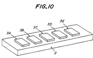
- Fig. 10 is a perspective view showing the arrangement of the piezoelectric device with which experiments were conducted.
- For the sake of convenience, same reference numerals are used throughout the entire figures to denote same or equivalent elements.
- Referring now to Figs. 1 to 4, there is shown a first embodiment of the unimorph-type piezoelectric device according to the present invention, which is denoted as a whole by reference numeral 1. The piezoelectric device 1 includes a locally thin-walled
ceramic substrate 2 and a plurality ofpiezoelectric transducers 3 arranged on the upper surface of thesubstrate 2. More particularly, thesubstrate 2 has a plurality of thin-walled regions 2a and thepiezoelectric transducers 3 are arranged on the thin-walled regions 2a. Thesubstrate 2 has a plurality ofclosed cavities 4 therein, each defined by aclosure wall 2b on the lower surface side of thesubstrate 2,peripheral walls 2c in thesubstrate 2 and a bottom wall on the upper surface side of thesubstrate 2, of which the bottom wall is constituted by the thin-walled region 2a of thesubstrate 2. Thebottom wall 2a functions as a diaphragm of thepiezoelectric transducer 3 in operation of the device 1. Thesubstrate 2 has relatively thick-walled regions 2d adjacent to the thin-walled regions 2a, where it is formed withgrooves 5 each arranged to extend along theperipheral wall 2c of thecavity 4 and to open at the upper surface of thesubstrate 2. - As shown in Fig. 2A, the
piezoelectric transducers 3 may be formed integrally with thesubstrate 2 by an ordinary film-formation process to be more fully described hereinafter, wherein alower electrode layer 3a, a film-shapedpiezoelectric layer 3b and anupper electrode layer 3c are sequentially laminated one above the other. As further shown in Figs. 3 and 4, thesubstrate 2 may be formed by known lamination process, wherein a lowergreen sheet 21 providing theclosure wall 2b of thesubstrate 2, an intermediategreen sheet 22 formed with window-like openings 22a corresponding to thecavity 4, and a thin-walled uppergreen sheet 23 providing thebottom wall 2a of thecavity 4, are sequentially laminated one above the other and subjected to a sintering to form an integrated substrate 2 (Fig. 4). - The particulars of the three
green sheets integrated substrate 2 will be explained below, with reference to Figs. 3 and 4. The uppergreen sheet 23 hasflat regions 23a corresponding to thebottom walls 2a of thesubstrate 2, and slit-like openings 23b extending through the uppergreen sheet 23 in the direction of its thickness. The intermediategreen sheet 22 has, besides the window-like openings 22a, slit-like grooves 22b with their bottoms situated close to the lowergreen sheet 21. The uppergreen sheet 23 and the intermediategreen sheet 22 are superimposed with each other so that the slit-like openings 23b in the uppergreen sheet 23 and the slit-like grooves 22b in the intermediategreen sheet 22 are brought into alignment with each other to form thegroove 5 in thesubstrate 2. When the piezoelectric device 1 is used as an actuator for an ink jet printing head, the lowergreen sheet 21 may have through-holes 21a to be used as an inlet which is in communication with an ink reservoir and/or as an outlet which is in communication with a discharge nozzle. - With further reference to Figs. 3 and 4, assuming by way of example that the
cavity 4 has a square contour, thegroove 5 in thesubstrate 2 has a length L which is at least 1/8, preferably 1/4 or more, of the length of the longitudinal edge of thecavity 4. Furthermore, as shown in Fig. 2A, thegroove 5 has a depth D1 which is substantially same as, or greater than the thickness t of the thin-walled bottom wall 2a of thecavity 4, and which preferably satisfies the following equation (1):
cavity 4. More preferably, the depth D1 of thegroove 5 satisfies the following equation (2):
- Advantageously, the
groove 5 has a width W1 as also shown in Fig. 2A, which is determined such that the width W2 of the thick-walled region 2d measured between the side wall of thegroove 5 and the oppositeperipheral wall 2c of thecavity 4 is within a range between 20 µm and 200 µm, preferably between 20 µm and 100 µm. When the width W2 of the thick-walled region 2d is less than 20 µm, the stiffness of the thick-walled region 2d is often excessively lowered, making it difficult to effectively induce the desired vertical displacement of thebottom wall 2a of thecavity 4 and thereby achieve an efficient voluminal change of thecavity 4. Moreover, cracks or the like defects tend to occur in the thick-walled region 2d during formation of thegroove 5, making it difficult to improve the manufacturing productivity of the piezoelectric device. When, on the other hand, the width W2 of the thick-walled region 2d is more than 200 µm, it becomes often difficult to achieve a sufficient stress relaxation during firing of the piezoelectric film layer, and hence to effectively improve the properties of the piezoelectric material. Moreover, due to the increased stiffness of the thick-walled region 2d, it becomes difficult to achieve a sufficient lateral displacement of theperipheral wall 2c of thecavity 4 thereby to enable a large voluminal change of thecavity 4. - It has to be noted in this connection that the above-mentioned preferred range of the width W2 is applicable also when two or
more grooves 5 are formed in each thick-walled region 2d of thesubstrate 2. - The
grooves 5 may have a square cross-section as shown in Figs. 2A and 4, or other appropriate cross-section such as V-shaped or trapezoid cross-section. - As for the thickness of the thin-
walled region 2a of thesubstrate 2, i.e., the bottom wall of thecavity 4, which functions as the diaphragm of thepiezoelectric transducer 3, in order to provide an improved high-speed response characteristic and a high conversion efficiency of thetransducer 3, the thin-walled region 2a has a thickness which is preferably 50 µm or less, more preferably 30 µm or less, and further more preferably 10 µm or less. - The piezoelectric device 1 according to the present invention includes
groove 5 in the relatively thick-walled region 2d of thesubstrate 2 adjacent to and surrounding theperipheral wall 2c of thecavity 4. It is therefore possible to provide a higher compliance of the relatively thick-walled substrate region 2d adjacent to theperipheral wall 2c of thecavity 4, with which the thin-walled regions 2a of thesubstrate 2 can be readily deformed upon firing shrinkage during manufacture of the device 1. This means that thetransducer 3 during manufacture of the device 1 can be subjected to the firing shrinkage in a relatively unrestricted sense, thereby minimizing the residual stresses in thetransducer 3 and assuring a highly improved operational characteristics of the device 1. As a result, it is possible to provide improved characteristics of thetransducer 3, including the relative dielectric constant, and to more fully make use of material properties which are inherent to the piezoelectric material. - As can be further appreciated from Fig. 2B, formation of the
grooves 5 in the thick-walled regions 2d of thesubstrate 2 ensures that the diaphragm of thepiezoelectric transducer 3 constituted by thebottom wall 2a of thecavity 4 can be sufficiently displaced vertically toward theclosure wall 2b, simultaneously inducing lateral displacements of the oppositeperipheral walls 2c toward the center of thecavity 4. A resultant higher compliance of the diaphragm of thepiezoelectric transducer 3, in combination with the lateral displacements of the oppositeperipheral walls 2c, permits a rapid voluminal change of the cavity and serves to provide a significantly increased discharge amount of ink from thecavity 4. - Moreover, when the piezoelectric device 1 according to the present invention includes an array of
piezoelectric transducers 3 formed on acommon substrate 2, thegrooves 5 formed in the relatively thick-walled regions 2d of thesubstrate 2 and situated between theadjacent transducers 3 provide a low vibration transmissibility of thesubstrate 2 between theadjacent transducers 3. Thegrooves 5 thus serve to effectively eliminate or suppress undesirable interaction or crosstalk betweenadjacent transducers 3, and to make it readily possible for the thin-walled regions 2a of thesubstrate 2 to achieve a uniform amount of the desired vertical displacement. Furthermore, even when neighbouringtransducers 3 are simultaneously actuated, thegroove 5 serves to absorb tensile forces between the transducers to thereby minimize the fluctuation in the vertical displacement amounts of the diaphragms. - For the sake of comparison, Figs. 5A and 5B schematically illustrate the operation of the piezoelectric device according to the above-mentioned U.S. Patent No. 5,210,455, which is provided with a plurality of
piezoelectric transducers ceramic substrate 2 havingopen cavities 4 which are not closed by a closure wall on the lower surface side of thesubstrate 2. - As shown in Fig. 5A, when only the
piezoelectric transducer 31 is actuated, thebottom wall 2a of thesubstrate 2 undergoes a vertical displacement which is assisted by slight lateral displacements of the thick-walled regions 2d forming the oppositeperipheral walls 2c of thecavity 4. However, when adjacentpiezoelectric transducers walled region 2d between thesetransducers bottom walls 2a of thesubstrate 2. The vertical displacement amount achieved by the diaphragm of the transducer in such operational state is reduced, as compared to the situation when a single transducer only is actuated. - When the piezoelectric device according to the present invention is used, e.g., as an actuator for an ink jet printing head, an insufficient vertical displacement amount of the diaphragm often results in a low ink discharge amount. It has been further found that the different displacement amount of the diaphragm depending upon the operational state of the device tends to cause fluctuation in the operational characteristics of the device. Moreover, due to the rigidity of the thick-
walled region 2d betweenadjacent transducers substrate 2 of the device 1 has a higher rigidity due to the formation of closed cavities which are closed by closure walls like that shown in Fig. 2A. - The present invention thus provides a unique solution for the above-mentioned problems, by forming at least one
groove 5 in the thick-walled region 2d of theceramic substrate 2. - A second embodiment of the unimorph-type piezoelectric device according to the present invention is shown in Figs. 6A, 6B and 6C, which is similar to, and directly comparable with the known device shown in Figs. 5A and 5B, in that the
substrate 2 hasopen cavities 4. Formation of thegrooves 5 in the thick-walled regions 2d of thesubstrate 2 makes it possible to provide a higher compliance of thediaphragm 2a and a resultant increased amount of its vertical displacement in operation of the device. As can be appreciated from Figs. 6B and 6C, thegrooves 5 between adjacent transducers serve to effectively suppress interaction or crosstalk between the transducers, and the vertical displacement amount of thediaphragm 2a can be uniformly maintained substantially uninfluenced by the operational state of the device, i.e., regardless of whether one transducer only is actuated (Fig. 6B) or adjacent transducers are simultaneously actuated (Fig. 6C). - A third embodiment of the unimorph-type piezoelectric device according to the present invention is shown in Fig. 7, in which each thick-
walled region 2d of thesubstrate 2 is relatively wide and formed with twogrooves bottom wall 2a of thecavity 4. This embodiment effectively provides an improved compliance of thediaphragm 2a of thepiezoelectric transducer 3, particularly when a plurality oftransducers 3 are arranged on thesubstrate 2 with a relatively wide pitch. - A fourth embodiment of the unimorph-type piezoelectric device according to the present invention is shown in Figs. 8 and 9, which is also provided with the
grooves 5 in the thick-walled regions 2d of thesubstrate 2. This embodiment is similar to the device disclosed in the applicants' copending U.S. Patent Application No. 08/206,939 or European Patent Application No. 94 301 633.7, of which the disclosure is here incorporated by reference. - More particularly, as shown in Fig. 9, the piezoelectric device 1 according to the illustrated embodiment includes
piezoelectric transducers 3 of which thepiezoelectric layer 3b has a dimension which is sufficient to substantially completely cover thelower electrode layer 3a. Thepiezoelectric layer 3b has at least oneedge 11 in the form of an extension protruding beyond thelower electrode layer 3a, which is at least locally incompletely bonded to theceramic substrate 2, as shown at 12. The term 'incomplete bond" as used herein refers to a specific bonded state between theceramic substrate 2 and at least oneedge 11 of thepiezoelectric layer 3b, which allows thepiezoelectric layer 3b to undergo a substantially unrestricted movement relative to thesubstrate 2. Adjacent to theedges 11 of thepiezoelectric layer 3b, there may be provided buffer resin layers 13 between theupper electrode layer 3c and thesubstrate 2, so as to provide a smooth and flexible connection of theupper electrode layer 3c to thesubstrate 2 and thereby protect theupper electrode layer 3c from possible damages due to impact or vibration during the production of the device or in the use condition. - The above-mentioned arrangement of the piezoelectric device 1 shown in Figs. 8 and 9 makes it readily possible to manufacture the piezoelectric device with an improved productivity, because it is not necessary to precisely align the edges of the
piezoelectric layer 3b with those of thelower electrode layer 3a. Theedges 11 of thepiezoelectric layer 3b of the device 1 shown in Figs. 8 and 9 serve to avoid short-circuit between the lower andupper electrode layers regions 12 between theceramic substrate 2 and theedge 11 of thepiezoelectric layer 3b protruding beyond thelower electrode layer 3a allows thepiezoelectric layer 3b to be moved relative to thesubstrate 2 in an unrestricted sense. It is thus possible to achieve satisfactory reliability and functions of the device, e.g., generation of large force or displacement, or of high output voltage level. - It should be noted that the present invention may also be applied to a piezoelectric device which includes a single piezoelectric transducer formed on the substrate. In this instance also, formation of the grooves in the thick-walled regions of the substrate adjacent to the thin-walled bottom wall of the cavity serve to provide a higher compliance of the bottom wall and hence significantly improved operational characteristics of the device.
- In order to realize highly improved operational characteristics of the piezoelectric device according to the present invention, the
substrate 2 preferably comprises zirconium oxide as a main component, having a crystal phase that has been completely or partially stabilized preferably by the addition of at least one compound selected from a group consisting of yttrium oxide, cerium oxide, magnesium oxide and calcium oxide. - The amount of the additives required for partially or completely stabilizing the zirconium oxide as described above may be 1-30 mol% for yttrium oxide, 6-50 mol% for cerium oxide, and 5-40 mol% for the magnesium oxide and calcium oxide. As for yttrium oxide in particular, the amount is preferably 2-7 mol%, more preferably 2-4 mol%, because the zirconium oxide added with the yttrium oxide of such amount has a partially stabilized crystal phase and thus exhibits particularly excellent substrate characteristics.
- A preferred method of forming the
ceramic substrate 2 with at least one cavity is to prepare a first green sheet having a desired thickness and at least one window-like opening formed by using a suitable mold, punching with a suitable die, or machining process, such as ultrasonic machining. A second, relatively thin green sheet is further prepared to have a thickness which corresponds to that of the thin-walled region of the substrate. The second green sheet is superimposed on the first green sheet under predetermined temperature/pressure condition, and then fired and integrated with each other. - The material for the
ceramic substrate 2 may contain a sintering aid, such as clay or the like. In this case, at least insofar as the second green sheet for the thin-walled region 2a is concerned, it is desirable to adjust the composition and amount of the sintering aid so that at least the sintered thin-walled region of the substrate does not contain a vitrous material such as silicone oxide, boron oxide, phosphorus oxide, germanium oxide, by an amount of 1% or more. This is because an excessive amount of vitrous material often results in undesirable reaction of the substrate material with the piezoelectric material during the heat treatment, making it difficult to control the composition of the piezoelectric material. - In the case of
ceramic substrate 2 wherein thecavity 4 for defining the thin-walled region 2a has a generally square contour, it is advantageous for thecavity 4 to have dimensions which are determined such that the length of the cavity is 2-20 times larger than its width. Furthermore, for assuring a sufficient amount of displacement or force to be generated by thepiezoelectric transducer 3, thetransducer 3 is formed on the thin-walled region 2a of thesubstrate 2 over an area which preferably corresponds to 50-95% of the width of thecavity 4. - In order that the
ceramic substrate 2 which has been formed as explained above permits satisfactory operational characteristics of thepiezoelectric transducer 3 formed thereon, it is advantageous to control the surface roughness Ra of thesubstrate 2 to be within a range of 0.03-0.9 µm. In this instance, the distortion or stress occurring in thepiezoelectric transducer 3 can be effectively transmitted to thesubstrate 2 having the above-mentioned range of the surface roughness Ra, and vice versa. Such a control of the surface roughness Ra is also effective to assure a high mechanical strength of the relatively thin substrate. - The green sheet for the
ceramic substrate 2 may be subjected to sintering at a temperature of 1,000°C to 1,800°C prior to formation of thepiezoelectric transducer 3. Alternatively, the green sheet for theceramic substrate 2 may be subjected to a suitable film-formation process to form thepiezoelectric transducer 3 and then sintered. Formation of thepiezoelectric transducer 3 on the previously sinteredceramic substrate 2 is often desirable in view of minimization of warp in the final product and dimensional accuracy of thepiezoelectric transducer 3. - The
groove 5 in the thick-walled region 2d of thesubstrate 2 may be formed either in the green sheet before the sintering step or in the already sintered substrate, by various methods. For example, the groove may be formed in the sintered substrate by an appropriate process such as laser beam process, electron beam process, slicing, blasting and ultrasonic process. Furthermore, the groove may be formed in the green sheet by press or punching with a suitable die. The groove formation process may be carried out either before or after the formation of the film-type piezoelectric transducer. Among others, the laser beam process is particularly suitable in that formation of grooves with a relatively complicated shape can be carried out in a facilitated manner. In this instance, it is advantageous to pay a particular attention to the process conditions so as to minimize thermal stress during the groove formation process, and thereby prevent formation of cracks in the ceramic substrate. From such a viewpoint, it has been confirmed that a suitable laser is a Nd-YAG laser having a Gaussian or normal energy distribution in the beam and using a TEM 00 single mode resonance. - Advantageously, for forming the groove in the thick-walled region of the ceramic substrate in accordance with the present invention, the laser beam process is performed by controlling the laser beam width to be 140 ns or less, preferably 100 ns or less, by carrying out a pulsation control by means of a Q-switch at a frequency of 3.6 kHz, for example, by concentrating the laser beam diameter to be 50 µm or less, preferably within a range of 5-10 µm, by means of an an appropriate concentration lens system, and by performing the process at a speed of 50 mm/sec or less.
- The
piezoelectric transducer 3 on theceramic substrate 2 comprising theelectrode layers piezoelectric layer 3b may be formed by a suitable film-formation process known, per se. That is to say, the film-fotmation process which may be applied to form thepiezoelectric transducer 3 of the device 1 according to the present invention includes a thick-film formation process such as screen printing, spraying, dipping or coating, and a thin-film formation process such as ion beam method, sputtering, vacuum vapor deposition, ion plating, chemical vapor deposition (CVD) or plating. In particular, the thick-film formation process can be advantageously applied to form a film-like piezoelectric layer. This is because the thick-film formation process makes it readily possible to form a film on the ceramic substrate by using a paste or slurry whose major component is powder of piezoelectric ceramic material. In this instance, when the powder of piezoelectric ceramic material has an average particle size within a range of 0.01 µm to 5 µm, preferably 0.05 µm to 3 µm, it is readily possible to realize excellent operational characteristics of the piezoelectric device. While the pattern of such a film may be formed by screen printing method or photolithography method, the pattern may also be formed by removing unnecessary regions of the film by laser cutting, slicing, ultrasonic machining or other suitable machining process. - The present invention is not limited to the specific construction, shape and/or pattern of the piezoelectric transducer illustrated in the drawings. For example, depending upon the utility of the piezoelectric device, the transducer may have triangular, rectangular or other polygonal shape, circular, elliptical or annular shape, comb- or lattice-like pattern, or any combination of these shapes and/or patterns.
- The electrode layers 3a, 3c and the
piezoelectric layer 3b formed on theceramic substrate 2 by a selected method as explained above may be either heat-treated in different steps for integration with the substrate each time a layer has been formed on the substrate, or simultaneously heat-treated in a single step for integration with the substrate after all the layers have been formed into a laminated structure on the substrate. When these methods are applied to manufacture the piezoelectric device as shown in Figs. 8 and 9, it is possible to incompletely bond the edges of thepiezoelectric layer 3b to theceramic substrate 2. When a film-formation process is used to form the electrode layers on the substrate or piezoelectric layer, it is not always a prerequisite condition to carry out the heat-treatment for integrating the film layers with the substrate or piezoelectric layer. Thus, for example, in order to provide an enhanced insulation between the twoelectrode layers piezoelectric film layer 3b, there may be instances wherein a coating of insulation resin or the like is provided on the periphery of thetransducer 3, or wherein dummy synthetic resin layers 13 as shown in Fig. 9 are formed on theceramic substrate 2, before formation of theupper electrode layer 3c. In these cases, theupper electrode layer 3c is preferably formed by a process which does not require heat-treatment. - The heat treatment temperature suitable for integrating the film layers 3a, 3b, 3c of the
piezoelectric transducer 3 and theceramic substrate 2 is generally within a range of 900-1,400°C, preferably 1,000-1,400°C. When thepiezoelectric film layer 3b is subjected to a heat-treatment, in order to stabilize the composition of the piezoelectric material and avoid undesirable change in the composition in a high temperature condition, the heat-treatment is preferably performed while controlling the atmosphere by heating the vaporization source of the piezoelectric material as well. It is also advantageous to use a method of firing the piezoelectric film layer while it is covered by a suitable cover member for preventing a direct exposure of the piezoelectric film layer to the firing atmosphere. In this case, the cover member consists preferably of a material which is similar to the ceramic substrate material. - The lower and
upper electrode layers piezoelectric transducer 3 may be formed of any electrically conductive material which can withstand the oxidizing firing and the heat-treatment atmosphere at a considerably high temperature condition as explained above. Thus, the electrode layers may be formed of a single metal, an alloy of metals, a mixture of metal or alloy with an electrically insulating ceramic material, e.g., TiO2, Al2O3, ZrO2, etc., or an electrically conductive ceramic material. However, it is preferable to use an electrode material whose major component is a noble metal having a high melting point, such as platinum, palladium, or rhodium, or an alloy such as silver-palladium, silver-platinum, platinum-palladium or the like. It is more preferable to use a cermet material of platinum and the ceramic material for the substrate, a cermet material of platinum and the ceramic material for the substrate and the piezoelectric material for the piezoelectric film layer, in view of an improved adhesion of the electrode layers to the piezoelectric film layer and/or the ceramic substrate. Among others, it is more preferable to use a material having a major component which comprises a platinum. - As for additive materials to be added to the electrode material, use of vitrous material such as silicon oxide should be avoided because such material tends to react with the piezoelectric material during the heat-treatment thereby deteriorating the characteristics of the piezoelectric device. The amount of the substrate material to be added to the electrode material is preferably 5-30% by volume, and the amount of the piezoelectric material to be added to the electrode material is preferably 5-20% by volume.
- The electrode layers 3a, 3c consisting of a conductive material as mentioned above may have a thickness of 20 µm or less, preferably 5 µm or less.
- The
piezoelectric layer 3b may be formed of any piezoelectric material which exhibits a relatively large amount of field-induced strain or displacement when applied with a voltage, due to the piezoelectric effect. The piezoelectric material may be either a crystalline material or an amorphous material, and may be a semi-conductive material or a dielectric or ferroelectric ceramic material. Furthermore, the piezoelectric material may either require an initial polarization or poling treatment or may not require such treatment. - Preferably, however, the piezoelectric materials which can be used in the present invention has a composition whose major component is lead zirconate titanate (PZT), lead magnesium niobate (PMN), lead nickel niobate (PNN), lead manganese niobate, lead antimony stannate, lead zinc niobate, lead titanate, lead zirconate or a mixture or solid solution thereof. Furthermore, the piezoelectric materials indicated above, whose major component is PZT or the like, may be added with a suitable amount of additives comprising an oxide or compound of lanthanum, barium, niobium, zinc, cerium, cadmium, chromium, cobalt, antimony, iron, yttrium, tantalum tungsten, nickel, manganese, lithium, strontium, calcium, and/or bismuth, so as to obtain a material whose major component is PLZT. However, addition of vitrous material such as silicon oxide should be avoided, since lead contained in the piezoelectric materials such as PZT tends to react with the vitrous material, making it difficult to achieve a desired composition of the piezoelectric film layer, thereby causing undesirable fluctuation and deterioration of the operational characteristics of the piezoelectric device.
- Among the piezoelectric materials indicated above, it is preferable to use material of which the major component comprises a mixture of lead magnesium niobate, lead zirconate and lead titanate, or a mixture of lead nickel niobate, lead magnesium niobate, lead zirconate and lead titanate. It is particularly advantageous to use a piezoelectric material of which the major component comprises a mixture of lead magnesium niobate, lead zirconate and lead titanate. Such a piezoelectric material has a particularly low reactivity with the substrate material during the heat-treatment, and is thus free from segregation of its components. Therefore, a suitable treatment for maintaining the composition serves to readily realize a desired composition or crystal structure. Furthermore, in the embodiment shown in Figs. 8 and 9, it becomes possible to maintain the edges of the
piezoelectric layer 3b protruding beyond thelower electrode layer 3a in such an incompletely bonded state with theceramic substrate 2 for assuring a proper operation of thepiezoelectric transducer 3. Moreover, such a piezoelectric material has a particularly high piezoelectric constant, and can be used as a material suitable for forming the piezoelectric film layer by the above-mentioned thick-film formation process such as screen printing, spraying, dipping, coating and the like. - While such multi-component piezoelectric material has a piezoelectric characteristic which varies depending upon the composition of components, a three-component material composed of lead magnesium niobate, lead zirconate and lead titanate, which can be suitably used in the invention, preferably has a composition in the vicinity of phase boundaries of a pseudo-cubic crystal phase, a tetragonal crystal phase and a rhombohedral crystal phase. To assure sufficiently high piezoelectric constant and electromechanical coupling factor, it is particularly advantageous to use a composition containing 15-50 mol% of lead magnesium niobate, 10-45 mol% of lead zirconate and 30-45 mol% of lead titanate.
- The piezoelectric transducer comprising the
electrode layers piezoelectric film layer 3b described above generally has a thickness of 100 µm or less. To assure a relatively large amount of displacement at a relatively low voltage, thepiezoelectric film layer 3b has a thickness which is preferably 50 µm or less, more preferably within a range of 3-40 µm. - In unimorph- or bimorph-type piezoelectric devices utilizing the transverse effect of the field-induced strain, when the piezoelectric material requires a poling treatment, it is a general practice to perform the treatment by applying a voltage between the upper and lower electrodes. In the case of the above-mentioned film-type piezoelectric device as in the present invention, it is preferable to perform the poling treatment with the upper electrode film layer used as a positive electrode. That is to say, in the case of the piezoelectric layer formed in accordance with the present invention, stresses generated in the piezoelectric layer during the sintering or heat treatment tend to form domains or orientations in a direction along the poling direction, which make it possible to subsequently perform an effective poling treatment.
- In order to confirm the advantageous functions of the present invention, comparative experiments have been carried out with a series of samples of the piezoelectric device, each having a substrate with cavities and five
piezoelectric transducers - Comparative sample S1 has open cavities such as that shown in Figs. 5A and 5B, and does not include grooves in the thick-walled regions of the substrate.
- Comparative sample S2 has closed cavities closed by a closure wall such as that shown in Figs. 2A and 2B, and does not include grooves in the thick-walled regions of the substrate.
- Comparative sample S3 has open cavities and includes shallow grooves in the thick-walled regions of the substrate, wherein each groove is arranged between adjacent transducers and has a depth which is substantially same as the thickness of the thin-walled region of the substrate.
- Sample of the invention S4 has closed cavities and include grooves in the thick-walled regions of the substrate, as shown in Figs. 2A and 2B, wherein each groove is arranged between adjacent transducers and has a depth of 100 µm which is greater than the thickness of the thin-walled region of the substrate.
- Sample of the invention S5 has closed cavities and include grooves in the thick-walled regions of the substrate, as shown in Figs. 2A and 2B, wherein each groove is arranged between adjacent transducers and has a depth of 50 µm which is greater than the thickness of the thin-walled region of the substrate.
- Sample of the invention S6 has closed cavities and include grooves in the thick-walled regions of the substrate, wherein two grooves are arranged between adjacent transducers as shown in Fig. 7, each having a depth of 100 µm which is greater than the thickness of the thin-walled region of the substrate.
- Each sample includes a substrate comprising a layer forming the peripheral wall of the cavity and having a thickness of 150 µm, which may be combined with a closure wall of a thickness of 150 µm, wherein the thickness of the thin-walled region is 10 µm.
- In the first place, using the comparative samples S1 and S2 and the sample of the invention S4, which were operated at the input voltage of 30V, the vertical displacement or deflection and relative dielectric constant were measured with respect to the
piezoelectric transducer 3C arranged at the center of the substrate. The measurement of the vertical displacement amount of thecenter transducer 3C has been carried out using a laser Doppler-type vibrometer. The result of the measurement is shown in Table 1 below.Table 1 Type of Sample Vertical Displacement (µm) Relative Dielectric Constant S1 0.29 2,700 S2 0.21 2,500 S4 0.28 3,400 - It can be appreciated from Table 1 that, with reference to the comparative sample S2 and the sample S4 of the invention, both including a substrate with closed cavities, the vertical displacement amount achieved by the
center transducer 3C of the sample S4 is higher than that achieved by thecenter transducer 3C of the comparative sample S2. With further reference to the sample S4 of the invention and the comparative sample S1 which includes a substrate with open cavities, even though the substrate of the sample S4 includes closed cavities, the vertical displacement amount achieved by thecenter transducer 3C of the sample S4 is substantially as high as that achieved by thecenter transducer 3C of the comparative sample S1. Moreover, the transducer of the sample S4 according to the invention exhibits the highest relative dielectric constant. This is believed due to the minimized residual stresses in the piezoelectric film layer and improved material characteristics thereof, both realized by the formation of the grooves in the thick-walled regions of the substrate and the resultant increased compliance of the thin-walled regions. - Experiments have been carried out with respect to the samples S1 to S6, to quantitatively measure the magnitude of interaction or crosstalk between adjacent piezoelectric transducers. This magnitude is defined as reduced displacement rate Dred(%), and expressed by the following formula:

Table 2 Type of Sample Reduced Deflection Rate Dred (%) of Transducers 3A 3B 3C 3D 3E S1 62 55 49 52 60 S2 85 75 70 74 85 S3 86 75 72 74 85 S4 95 90 89 91 94 S5 90 81 81 82 91 S6 97 95 94 94 98 - It can be appreciated from Table 2 that, with reference to the comparative samples S1 to S3, simultaneous operation of adjacent transducers tends to reduce the displacement of each transducer and enhance the fluctuation of the reduced displacement rate Dred. In contrast, with reference to the samples S4 to S6 of the invention, simultaneous operation of adjacent transducers does not result in a significant reduction of the displacement of each transducer and fluctuation of the reduced displacement rate Dred. Thus, the present invention makes it possible to suppress the interaction or crosstalk between adjacent piezoelectric transducers. With reference to the comparative samples S2 and S3, suppression of the interaction or crosstalk between adjacent piezoelectric transducers is still insufficient in the case of grooves of which the depth is substantially same as the thickness of the thin-walled regions. With reference to the samples S4 and S5 of the invention, a greater depth of the groove serves to more effectively suppress the interaction or crosstalk between adjacent piezoelectric transducers. With further reference to the samples S4 and S6 of the invention, formation of two grooves between adjacent transducers results in even more effective suppression of the interaction or crosstalk between adjacent piezoelectric transducers.
- It will be readily appreciated from the foregoing detailed description that the piezoelectric device according to the present invention features the formation of at least one groove in the relatively thick-walled region of the substrate adjacent to and surrounding the peripheral wall of the cavity. It is thus possible to provide a higher compliance of the relatively thick-walled substrate region adjacent to the peripheral wall of the cavity, with which the thin-walled regions of the substrate can be readily deformed upon firing shrinkage during manufacture of the device. Therefore, despite the difference in the coefficient of thermal expansion of the materials for the substrate and the piezoelectric transducer, the transducer during manufacture of the device can be subjected to the firing shrinkage in a relatively unrestricted sense, thereby minimizing the residual stresses in the transducer and assuring a highly improved operational characteristics of the device.
- Moreover, when the piezoelectric device according to the present invention includes an array of piezoelectric transducers formed on a common substrate, the grooves in the relatively thick-walled region of the substrate serves to effectively eliminate or suppress interaction or crosstalk between the transducers, and makes it readily possible to uniformly achieve a desired amount of displacement of the thin-walled regions'of the substrate in a direction perpendicular to the general surface of the substrate.
- While the present invention has been described with reference to some preferred embodiments, they were given by way of examples only.
Claims (10)
- A piezoelectric device comprising a ceramic substrate (2) with an outer surface, said substrate being locally formed with at least one cavity (4) defined by at least one peripheral wall surface and a bottom wall surface, said bottom wall surface being a surface, opposite to said outer surface, of a reduced thickness bottom wall region (2a) and said peripheral wall surface being a surface of a thick-walled region (2d) adjacent and surrounding said cavity (4), said device further comprising at least one film-type piezoelectric transducer (3) formed integrally with the substrate (2) and arranged on said outer surface opposite to said bottom wall surface, characterized in that said thick-walled region is formed with at least one groove (5) extending alongside said peripheral wall surface and having a depth which is greater than the thickness of said bottom wall region, said groove (5) being arranged so as to permit simultaneous displacements of said bottom wall region (2a) and said thick-walled region (2d) between said cavity (4) and said groove (5), thereby to cause a volume change of said cavity (4).
- A piezoelectric device as claimed in claim 1, wherein said ceramic substrate (2) comprises zirconium oxide as a major component, said zirconium oxide having a completely or partially stabilized zirconium oxide crystal phase.
- A piezoelectric device as claimed in claim 2, wherein said zirconium oxide has a zirconium oxide crystal phase which has been completely or partially stabilized by addition of at least one of yttrium oxide, cerium oxide, magnesium oxide and calcium oxide.
- The piezoelectric device of claim 1, 2 or 3 wherein said thickness of the bottom wall region (2a) is 50 µm or less.
- The piezoelectric device of any one of claims 1 to 4, wherein said piezoelectric transducer (3) comprises a first electrode layer (3a), a piezoelectric layer (3b) and a second electrode layer (3c) which are sequentially laminated with each other.
- A piezoelectric device as claimed in claim 5, wherein said piezoelectric layer (3b) comprises a material having as a major component a mixture of lead magnesium niobate, lead zirconate and lead titanate.
- A piezoelectric device as claimed in claim 5, wherein said piezoelectric layer comprises a material having as a major component a mixture of lead nickel niobate, lead magnesium niobate, lead zirconate and lead titanate.
- The piezoelectric device of any one of claims 1 to 7, wherein said ceramic substrate (2) comprises a first layer (22) formed with at least one window-like opening (22a), and a second layer (23) on one side of said first layer (22), said opening (22a) in the first layer having a periphery which provides said peripheral wall surface of the cavity (4), and said second layer (23) closing one side of said opening (22a) in the first layer and thereby providing said bottom wall surface of said cavity (4).
- The piezoelectric device of any one of claims 1 to 7, wherein said ceramic substrate (2) comprises a first layer (22) formed with at least one window-like opening (22a) and a second layer (23) on one side of said first layer (22), said opening (22a) in the first layer having a periphery which provides said peripheral wall surface of the cavity (4), and said second layer (23) closing one side of said opening (22a) in the first layer and thereby providing said bottom wall surface of said cavity (4), and wherein said ceramic substrate further comprises a third layer (21) on the opposite side of said first layer (22) from said second layer (23), said third layer (21) at least partly closing another side of said opening (22a) in the first layer.
- The piezoelectric device of any one of claims 1 to 7, wherein said ceramic substrate comprises a first layer formed with at least one thin-walled region for defining said cavity, and a second layer on said first layer on the side of an inner surface of the substrate, for closing said cavity in the first layer.
Applications Claiming Priority (2)
| Application Number | Priority Date | Filing Date | Title |
|---|---|---|---|
| JP163945/93 | 1993-06-08 | ||
| JP16394593A JP3318687B2 (en) | 1993-06-08 | 1993-06-08 | Piezoelectric / electrostrictive film element and method of manufacturing the same |
Publications (2)
| Publication Number | Publication Date |
|---|---|
| EP0629007A1 EP0629007A1 (en) | 1994-12-14 |
| EP0629007B1 true EP0629007B1 (en) | 1997-03-05 |
Family
ID=15783811
Family Applications (1)
| Application Number | Title | Priority Date | Filing Date |
|---|---|---|---|
| EP94304112A Expired - Lifetime EP0629007B1 (en) | 1993-06-08 | 1994-06-08 | Piezoelectric device |
Country Status (6)
| Country | Link |
|---|---|
| US (1) | US6584660B1 (en) |
| EP (1) | EP0629007B1 (en) |
| JP (1) | JP3318687B2 (en) |
| DE (1) | DE69401855T2 (en) |
| HK (1) | HK117197A (en) |
| SG (1) | SG66279A1 (en) |
Families Citing this family (78)
| Publication number | Priority date | Publication date | Assignee | Title |
|---|---|---|---|---|
| JP3501860B2 (en) * | 1994-12-21 | 2004-03-02 | 日本碍子株式会社 | Piezoelectric / electrostrictive film type element and manufacturing method thereof |
| FR2730362A1 (en) * | 1995-02-06 | 1996-08-09 | Thomson Csf | TRANSDUCER IN MATERIAL WITH ELECTROMECHANICAL TRANSFORMATION, APPLICATION TO MICROACTIONERS AND METHOD OF MAKING SAME |
| JP3439570B2 (en) * | 1995-05-08 | 2003-08-25 | 日本碍子株式会社 | Diaphragm structure |
| JP3465427B2 (en) * | 1995-07-28 | 2003-11-10 | ソニー株式会社 | Piezoelectric actuator and method of manufacturing the same |
| JP3432974B2 (en) * | 1995-10-13 | 2003-08-04 | 日本碍子株式会社 | Piezoelectric / electrostrictive film type element |
| JPH11191645A (en) * | 1997-12-25 | 1999-07-13 | Kyocera Corp | Piezoelectric-electrostrictive film actuator |
| US6335586B1 (en) * | 1998-12-28 | 2002-01-01 | Ngk Insulators, Ltd. | Piezoelectric/electrostrictive device and production method thereof |
| JP2000348321A (en) * | 1999-06-03 | 2000-12-15 | Nec Corp | Magnetic disk device, magnetic head, manufacture of magnetic head, and manufacture of magnetic disk device |
| EP1089355B1 (en) * | 1999-10-01 | 2006-11-22 | Ngk Insulators, Ltd. | Piezoelectric/electrostrictive device |
| US6915547B2 (en) | 1999-10-01 | 2005-07-12 | Ngk Insulators, Ltd. | Piezoelectric/electrostrictive device and method of manufacturing same |
| US7164221B1 (en) | 1999-10-01 | 2007-01-16 | Ngk Insulators, Ltd. | Piezoelectric/electrostrictive device and method of manufacturing same |
| WO2001072520A1 (en) * | 2000-03-27 | 2001-10-04 | Fujitsu Limited | Multiple-nozzle ink-jet head and method of manufacture thereof |
| JP3768789B2 (en) * | 2000-09-07 | 2006-04-19 | アルプス電気株式会社 | Ultrasonic vibrator, wet processing nozzle and wet processing apparatus |
| JP3465675B2 (en) * | 2000-09-11 | 2003-11-10 | 日本碍子株式会社 | Piezoelectric / electrostrictive film type element |
| EP1340970A4 (en) * | 2000-11-06 | 2007-06-27 | Jtekt Corp | Mechanical quantity sensor element, load sensor element, acceleration sensor element, and pressure sensor element |
| WO2002073710A1 (en) * | 2001-03-12 | 2002-09-19 | Ngk Insulators,Ltd. | Piezoelectric/electrostrictive film type actuator and method of manufacturing the actuator |
| US6794723B2 (en) * | 2001-09-12 | 2004-09-21 | Ngk Insulators, Ltd. | Matrix type piezoelectric/electrostrictive device and manufacturing method thereof |
| JP3908512B2 (en) * | 2001-11-16 | 2007-04-25 | セイコーインスツル株式会社 | Piezoelectric transducer and pulse wave detector |
| JP3991894B2 (en) * | 2002-03-18 | 2007-10-17 | セイコーエプソン株式会社 | Piezoelectric actuator manufacturing method, liquid jet head manufacturing method, and actuator base member |
| JP3903936B2 (en) * | 2002-03-18 | 2007-04-11 | セイコーエプソン株式会社 | Piezoelectric element, piezoelectric actuator, and liquid jet head |
| US7019438B2 (en) * | 2002-06-21 | 2006-03-28 | Ngk Insulators, Ltd. | Piezoelectric/electrostrictive film device |
| US7067961B2 (en) * | 2002-07-12 | 2006-06-27 | Ngk Insulators, Ltd. | Piezoelectric/electrostrictive film device, and manufacturing method of the device |
| JP2004064067A (en) * | 2002-07-26 | 2004-02-26 | Ngk Insulators Ltd | Piezoelectric / electrostrictive film element |
| JP4447250B2 (en) * | 2002-08-07 | 2010-04-07 | 日本碍子株式会社 | Piezoelectric actuator array and manufacturing method |
| JP4422973B2 (en) * | 2002-08-27 | 2010-03-03 | 京セラ株式会社 | Multilayer piezoelectric body, actuator, and print head |
| US6987348B2 (en) * | 2002-12-13 | 2006-01-17 | Palo Alto Research Center Inc. | Piezoelectric transducers |
| US6967431B2 (en) * | 2002-12-13 | 2005-11-22 | Palo Alto Research Center Inc. | Piezoelectric transducers and methods of manufacture |
| US6843771B2 (en) * | 2003-01-15 | 2005-01-18 | Salutron, Inc. | Ultrasonic monitor for measuring heart rate and blood flow rate |
| US20060152375A1 (en) * | 2003-01-16 | 2006-07-13 | Matsushita Electric Industrial Co., Ltd. | Pressure-sensitive sensor and object detector |
| US7270404B2 (en) * | 2003-09-24 | 2007-09-18 | Fujifilm Corporation | Inkjet recording head, inkjet recording apparatus and method for manufacturing inkjet recording head |
| JP2005103771A (en) * | 2003-09-26 | 2005-04-21 | Fuji Photo Film Co Ltd | Inkjet head, manufacturing method therefor and inkjet recording device |
| JP2005104038A (en) * | 2003-09-30 | 2005-04-21 | Fuji Photo Film Co Ltd | Discharge head and liquid discharge device |
| US7048361B2 (en) | 2003-11-05 | 2006-05-23 | Xerox Corporation | Ink jet apparatus |
| US7375911B1 (en) * | 2003-11-25 | 2008-05-20 | Maxtor Corporation | Piezoelectric actuator and sensor for disk drive dual-stage servo systems |
| US7585061B2 (en) * | 2004-08-27 | 2009-09-08 | Fujifilm Corporation | Ejection head and image forming apparatus |
| JP4504237B2 (en) * | 2005-03-18 | 2010-07-14 | 富士通株式会社 | Wet etching method, micro movable element manufacturing method, and micro movable element |
| US7449816B2 (en) * | 2005-03-25 | 2008-11-11 | Brother Kogyo Kabushiki Kaisha | Piezoelectric actuator, liquid transporting apparatus, and method for producing piezoelectric actuator and method for producing liquid transporting apparatus |
| JP4630998B2 (en) * | 2005-05-31 | 2011-02-09 | 独立行政法人産業技術総合研究所 | Speaker device or microphone device |
| US7535373B2 (en) * | 2005-07-15 | 2009-05-19 | Honeywell International, Inc. | Security techniques for electronic devices |
| JP4597105B2 (en) * | 2005-09-12 | 2010-12-15 | 日本碍子株式会社 | Speaker and power generator |
| US20070120896A1 (en) * | 2005-11-30 | 2007-05-31 | Xerox Corporation | Drop generator |
| JP4618165B2 (en) * | 2006-03-06 | 2011-01-26 | 株式会社デンソー | Ultrasonic sensor |
| EP1842676A3 (en) * | 2006-04-06 | 2009-06-17 | Océ-Technologies B.V. | Printhead and inkjet printer comprising such a printhead |
| US20070236541A1 (en) * | 2006-04-06 | 2007-10-11 | Oce-Technologies B.V. | Printhead and inkjet printer comprising such a printhead |
| JP4091641B2 (en) * | 2006-04-07 | 2008-05-28 | 富士フイルム株式会社 | Piezoelectric element, manufacturing method thereof, and ink jet recording head |
| US7608983B2 (en) * | 2006-07-18 | 2009-10-27 | Brother Kogyo Kabushiki Kaisha | Piezoelectric actuator, liquid transporting apparatus, and liquid-droplet jetting apparatus |
| JP5223255B2 (en) * | 2006-07-18 | 2013-06-26 | ブラザー工業株式会社 | Piezoelectric actuator, liquid transfer device, and droplet ejection device |
| US7950782B2 (en) * | 2006-12-21 | 2011-05-31 | Seiko Epson Corporation | Droplet discharging head, energy converter, piezoelectric device, MEMS structure, cantilever actuator, piezoelectric sensor, and piezoelectric linear motor |
| US7851970B2 (en) * | 2006-12-22 | 2010-12-14 | The Charles Stark Draper Laboratory, Inc. | Structures for crystal packaging including flexible membranes |
| US20080246367A1 (en) * | 2006-12-29 | 2008-10-09 | Adaptivenergy, Llc | Tuned laminated piezoelectric elements and methods of tuning same |
| US7786653B2 (en) * | 2007-07-03 | 2010-08-31 | Northrop Grumman Systems Corporation | MEMS piezoelectric switch |
| US7854497B2 (en) | 2007-10-30 | 2010-12-21 | Hewlett-Packard Development Company, L.P. | Fluid ejection device |
| US8379888B2 (en) | 2008-01-18 | 2013-02-19 | National Taiwan University | Flexible piezoelectric sound-generating devices |
| JPWO2009119707A1 (en) * | 2008-03-26 | 2011-07-28 | 日本碍子株式会社 | Droplet discharge device and method for manufacturing droplet discharge device |
| US20110242168A1 (en) * | 2008-09-30 | 2011-10-06 | Fujifilm Corporation | Method for Nozzle Velocity Control |
| JP2012504072A (en) * | 2008-09-30 | 2012-02-16 | フジフィルム ディマティックス, インコーポレイテッド | Control of nozzle flow rate |
| JP2010143205A (en) * | 2008-12-22 | 2010-07-01 | Seiko Epson Corp | Liquid jet head and liquid jet apparatus, and actuator apparatus |
| US8525279B2 (en) * | 2009-06-04 | 2013-09-03 | University Of Louisville Research Foundation, Inc. | Single element three terminal piezoresistive pressure sensor |
| KR101101467B1 (en) * | 2009-07-28 | 2012-01-03 | 삼성전기주식회사 | Inkjet head and method of menufacturing inkjet head |
| US8484823B2 (en) * | 2009-08-28 | 2013-07-16 | The Charles Stark Draper Laboratory, Inc. | Methods and apparatus for mounting a crystal |
| JP5754129B2 (en) * | 2010-03-11 | 2015-07-29 | セイコーエプソン株式会社 | Piezoelectric element, piezoelectric sensor, electronic device, and method of manufacturing piezoelectric element |
| JP5677780B2 (en) * | 2010-07-28 | 2015-02-25 | 日本セラミック株式会社 | Ultrasonic transceiver |
| KR20120080882A (en) * | 2011-01-10 | 2012-07-18 | 삼성전자주식회사 | Acoustic transducer and method of driving the same |
| JP6158822B2 (en) * | 2011-11-30 | 2017-07-05 | オセ−テクノロジーズ ビーブイ | Ink jet print head and manufacturing method thereof |
| US20130342488A1 (en) * | 2012-06-26 | 2013-12-26 | Kent Displays Incorporated | Cholesteric liquid crystal writing tablet erased by a piezoelectric transducer |
| CN104883979B (en) * | 2012-12-26 | 2017-05-03 | 富士胶片株式会社 | Unimorph type ultrasound probe and method for fabricating same |
| WO2015131083A1 (en) * | 2014-02-28 | 2015-09-03 | The Regents Of The University Of California | Variable thickness diaphragm for a wideband robust piezoelectric micromachined ultrasonic transducer (pmut) |
| JP2016033970A (en) | 2014-07-31 | 2016-03-10 | セイコーエプソン株式会社 | Ultrasonic device and method for manufacturing the same, and probe and electronic equipment |
| JP2017019168A (en) * | 2015-07-09 | 2017-01-26 | 東芝テック株式会社 | Inkjet head and manufacturing method of the same |
| US10888897B2 (en) | 2016-10-27 | 2021-01-12 | Cts Corporation | Transducer, transducer array, and method of making the same |
| US11039814B2 (en) * | 2016-12-04 | 2021-06-22 | Exo Imaging, Inc. | Imaging devices having piezoelectric transducers |
| CN110603817B (en) * | 2017-05-09 | 2020-08-25 | 富士胶片株式会社 | Piezoelectric microphone chip and piezoelectric microphone |
| US10648852B2 (en) | 2018-04-11 | 2020-05-12 | Exo Imaging Inc. | Imaging devices having piezoelectric transceivers |
| US10699741B1 (en) * | 2019-01-08 | 2020-06-30 | International Business Machines Corporation | Multi-channel magnetic recording head having compliantly encapsulated transducers |
| US11794209B2 (en) | 2019-09-12 | 2023-10-24 | Exo Imaging, Inc. | Increased MUT coupling efficiency and bandwidth via edge groove, virtual pivots, and free boundaries |
| JP2022047304A (en) * | 2020-09-11 | 2022-03-24 | 株式会社リコー | Liquid discharge head and liquid discharge apparatus |
| US11951512B2 (en) | 2021-03-31 | 2024-04-09 | Exo Imaging, Inc. | Imaging devices having piezoelectric transceivers with harmonic characteristics |
| US11819881B2 (en) | 2021-03-31 | 2023-11-21 | Exo Imaging, Inc. | Imaging devices having piezoelectric transceivers with harmonic characteristics |
Family Cites Families (10)
| Publication number | Priority date | Publication date | Assignee | Title |
|---|---|---|---|---|
| JPS5942193A (en) * | 1982-09-02 | 1984-03-08 | Toshiba Corp | Laser scribing method |
| US4551647A (en) * | 1983-03-08 | 1985-11-05 | General Electric Company | Temperature compensated piezoelectric transducer and lens assembly and method of making the assembly |
| JPS60111600A (en) | 1983-11-21 | 1985-06-18 | Mitsubishi Mining & Cement Co Ltd | Electromechanical transducing element |
| US4641153A (en) * | 1985-09-03 | 1987-02-03 | Pitney Bowes Inc. | Notched piezo-electric transducer for an ink jet device |
| DE3630206A1 (en) * | 1985-09-06 | 1987-03-19 | Fuji Electric Co Ltd | INK JET PRINT HEAD |
| JPH01188350A (en) * | 1988-01-25 | 1989-07-27 | Fuji Electric Co Ltd | Manufacture of ink jet recording head |
| JP2806386B2 (en) * | 1988-02-16 | 1998-09-30 | 富士電機株式会社 | Inkjet recording head |
| DE68906001T2 (en) * | 1988-12-07 | 1993-09-09 | Seiko Epson Corp | On-demand inkjet print head. |
| US5057664A (en) * | 1989-10-20 | 1991-10-15 | Electro Scientific Industries, Inc. | Method and apparatus for laser processing a target material to provide a uniformly smooth, continuous trim profile |
| US5210455A (en) * | 1990-07-26 | 1993-05-11 | Ngk Insulators, Ltd. | Piezoelectric/electrostrictive actuator having ceramic substrate having recess defining thin-walled portion |
-
1993
- 1993-06-08 JP JP16394593A patent/JP3318687B2/en not_active Expired - Lifetime
-
1994
- 1994-06-08 US US08/257,020 patent/US6584660B1/en not_active Expired - Fee Related
- 1994-06-08 EP EP94304112A patent/EP0629007B1/en not_active Expired - Lifetime
- 1994-06-08 SG SG1996007142A patent/SG66279A1/en unknown
- 1994-06-08 DE DE69401855T patent/DE69401855T2/en not_active Expired - Lifetime
-
1997
- 1997-06-26 HK HK117197A patent/HK117197A/en not_active IP Right Cessation
Also Published As
| Publication number | Publication date |
|---|---|
| US6584660B1 (en) | 2003-07-01 |
| JP3318687B2 (en) | 2002-08-26 |
| DE69401855D1 (en) | 1997-04-10 |
| HK117197A (en) | 1997-09-05 |
| SG66279A1 (en) | 1999-07-20 |
| DE69401855T2 (en) | 1997-07-31 |
| EP0629007A1 (en) | 1994-12-14 |
| JPH06350155A (en) | 1994-12-22 |
Similar Documents
| Publication | Publication Date | Title |
|---|---|---|
| EP0629007B1 (en) | Piezoelectric device | |
| EP0615294B1 (en) | Piezoelectric device | |
| EP0606767B1 (en) | Piezoelectric device | |
| EP1148561B1 (en) | Piezoelectric/electrostrictive film type elements and process for producing the same | |
| EP0782203B1 (en) | Piezoelectric/electrostrictive film-type element and method for producing the same | |
| EP0526048B1 (en) | Piezoelectric/electrostrictive element having ceramic substrate formed essentially of stabilized zirconia | |
| KR100715406B1 (en) | Piezoelectric structure, liquid ejecting head and manufacturing method therefor | |
| EP0656665B1 (en) | Piezoelectric device | |
| EP0468796B1 (en) | Piezoelectric/electrostrictive actuator having ceramic substrate | |
| EP0587346B1 (en) | Ink jet print head having members with different coefficients of thermal expansion | |
| EP0667646A1 (en) | Piezoelectric/electrostrictive film element and method of producing the same | |
| EP0766325B1 (en) | Piezoelectric/electrostrictive film element and method of producing the same | |
| EP0561616B1 (en) | Piezoelectric/electrostrictive element having auxiliary electrode disposed between piezoelectric/electrostrictive layer and substrate | |
| EP1489668B1 (en) | Piezoelectric/electrostrictive device made of piezoelectric/electrostrictive film and manufacturing method | |
| EP0718900A2 (en) | Piezoelectric/electrostrictive film element with a diaphragm having at least one stress releasing end section | |
| US6246156B1 (en) | Piezoelectric/electrostrictive element | |
| JPH0549270A (en) | Piezoelectric/electrostrictive actuator | |
| JP3282085B2 (en) | Method for manufacturing piezoelectric / electrostrictive film element |
Legal Events
| Date | Code | Title | Description |
|---|---|---|---|
| PUAI | Public reference made under article 153(3) epc to a published international application that has entered the european phase |
Free format text: ORIGINAL CODE: 0009012 |
|
| AK | Designated contracting states |
Kind code of ref document: A1 Designated state(s): DE FR GB IT |
|
| 17P | Request for examination filed |
Effective date: 19950316 |
|
| RAP1 | Party data changed (applicant data changed or rights of an application transferred) |
Owner name: SEIKO EPSON CORPORATION Owner name: NGK INSULATORS, LTD. |
|
| 17Q | First examination report despatched |
Effective date: 19960208 |
|
| GRAG | Despatch of communication of intention to grant |
Free format text: ORIGINAL CODE: EPIDOS AGRA |
|
| GRAH | Despatch of communication of intention to grant a patent |
Free format text: ORIGINAL CODE: EPIDOS IGRA |
|
| GRAH | Despatch of communication of intention to grant a patent |
Free format text: ORIGINAL CODE: EPIDOS IGRA |
|
| GRAA | (expected) grant |
Free format text: ORIGINAL CODE: 0009210 |
|
| AK | Designated contracting states |
Kind code of ref document: B1 Designated state(s): DE FR GB IT |
|
| REF | Corresponds to: |
Ref document number: 69401855 Country of ref document: DE Date of ref document: 19970410 |
|
| ITF | It: translation for a ep patent filed |
Owner name: MODIANO & ASSOCIATI S.R.L. |
|
| ET | Fr: translation filed | ||
| PLBE | No opposition filed within time limit |
Free format text: ORIGINAL CODE: 0009261 |
|
| STAA | Information on the status of an ep patent application or granted ep patent |
Free format text: STATUS: NO OPPOSITION FILED WITHIN TIME LIMIT |
|
| 26N | No opposition filed | ||
| REG | Reference to a national code |
Ref country code: GB Ref legal event code: IF02 |
|
| PGFP | Annual fee paid to national office [announced via postgrant information from national office to epo] |
Ref country code: GB Payment date: 20130605 Year of fee payment: 20 Ref country code: DE Payment date: 20130605 Year of fee payment: 20 |
|
| PGFP | Annual fee paid to national office [announced via postgrant information from national office to epo] |
Ref country code: IT Payment date: 20130619 Year of fee payment: 20 Ref country code: FR Payment date: 20130624 Year of fee payment: 20 |
|
| REG | Reference to a national code |
Ref country code: DE Ref legal event code: R071 Ref document number: 69401855 Country of ref document: DE |
|
| REG | Reference to a national code |
Ref country code: DE Ref legal event code: R071 Ref document number: 69401855 Country of ref document: DE |
|
| REG | Reference to a national code |
Ref country code: GB Ref legal event code: PE20 Expiry date: 20140607 |
|
| PG25 | Lapsed in a contracting state [announced via postgrant information from national office to epo] |
Ref country code: GB Free format text: LAPSE BECAUSE OF EXPIRATION OF PROTECTION Effective date: 20140607 |
|
| PG25 | Lapsed in a contracting state [announced via postgrant information from national office to epo] |
Ref country code: DE Free format text: LAPSE BECAUSE OF EXPIRATION OF PROTECTION Effective date: 20140611 |