EP0617852B1 - Vorrichtung und verfahren zur steuerung der temperaturabhängigkeit des ein/aus-verhältnisses einer laserdiode - Google Patents
Vorrichtung und verfahren zur steuerung der temperaturabhängigkeit des ein/aus-verhältnisses einer laserdiode Download PDFInfo
- Publication number
- EP0617852B1 EP0617852B1 EP93902712A EP93902712A EP0617852B1 EP 0617852 B1 EP0617852 B1 EP 0617852B1 EP 93902712 A EP93902712 A EP 93902712A EP 93902712 A EP93902712 A EP 93902712A EP 0617852 B1 EP0617852 B1 EP 0617852B1
- Authority
- EP
- European Patent Office
- Prior art keywords
- laser
- voltage
- output power
- power level
- lasc
- Prior art date
- Legal status (The legal status is an assumption and is not a legal conclusion. Google has not performed a legal analysis and makes no representation as to the accuracy of the status listed.)
- Expired - Lifetime
Links
- 230000008033 biological extinction Effects 0.000 title claims abstract description 22
- 238000000034 method Methods 0.000 title claims description 8
- 238000012549 training Methods 0.000 claims abstract description 10
- 230000003247 decreasing effect Effects 0.000 claims abstract description 7
- 230000003287 optical effect Effects 0.000 claims description 13
- 230000005540 biological transmission Effects 0.000 claims description 6
- 230000005855 radiation Effects 0.000 claims 5
- 230000001419 dependent effect Effects 0.000 claims 1
- 230000000306 recurrent effect Effects 0.000 claims 1
- 230000008859 change Effects 0.000 abstract description 4
- NJPPVKZQTLUDBO-UHFFFAOYSA-N novaluron Chemical compound C1=C(Cl)C(OC(F)(F)C(OC(F)(F)F)F)=CC=C1NC(=O)NC(=O)C1=C(F)C=CC=C1F NJPPVKZQTLUDBO-UHFFFAOYSA-N 0.000 description 13
- 239000000835 fiber Substances 0.000 description 3
- 230000007423 decrease Effects 0.000 description 2
- 238000012544 monitoring process Methods 0.000 description 2
- 206010065929 Cardiovascular insufficiency Diseases 0.000 description 1
- 230000032683 aging Effects 0.000 description 1
- 230000003679 aging effect Effects 0.000 description 1
- 230000002457 bidirectional effect Effects 0.000 description 1
- 238000005259 measurement Methods 0.000 description 1
- 238000012986 modification Methods 0.000 description 1
- 230000004048 modification Effects 0.000 description 1
- 239000013307 optical fiber Substances 0.000 description 1
- 230000004044 response Effects 0.000 description 1
- 230000035945 sensitivity Effects 0.000 description 1
- 230000032258 transport Effects 0.000 description 1
Images




Definitions
- the present invention relates to an apparatus for controlling an output of a laser diode over temperature so as to control and optimally maintain constant its extinction ratio, and a method for initially setting HIGH and LOW outputs of the laser diode so as to have a desired extinction ratio.
- FIG 1 illustrates various characteristic curves for a laser diode whereby current I versus power P is graphed, the three curves illustrating data for a laser diode at three distinct temperatures.
- a pedestal bias current 4 of the laser diode increases with temperature.
- One method of controlling an output of a laser diode is to incorporate a thermoelectric cooler into a laser package so as to keep the diode at a constant temperature so that its pedestal bias current remains constant. Accordingly, an extinction ratio of the laser diode, defined as the ratio between its HIGH power output divided by its LOW power output can easily be maintained constant.
- a disadvantage of such proposals is that thermoelectric cooler designs tend to increase the laser cost, and decreases reliability of the laser diode since any failure in the thermoelectric cooler device or its circuitry will result in the applied bias current being inappropriate as the temperature of the laser diode varies.
- EP-A-0 428 016 discloses a method and an apparatus for controlling the modulating current of a laser diode. This apparatus controls the modulating current in such a way that the slope ratio between the bias (logical 0) and the modulating (logical 1) operating points is fixed. Neither the actual laser output power levels nor the extinction ratio therebetween are controlled.
- US-A-4,995,105 discloses a laser diode driver circuit for laser scanners which allows the continuous calibration of a laser so that the output power of the laser is accurately modulated by the input video signal regardless of temperature changes or aging effects of the laser.
- the circuit comprises two independent control loops for measuring the light output of the laser. By one of the control loops the low output is measured and compared to a reference, wherein the error therebetween is used to adjust the bias current of the laser. By the other control loop the difference between the low and high laser outputs is measured and compared to a second reference, wherein the error therebetween is used to adjust the gain of the video signal so that the difference between said low and high outputs is maintained constant.
- US-A-4,985,896 discloses a laser driving device capable of providing a stable laser emission regardless of the ambient temperature by supplying the laser with a first current and a second bias current with controlled ratio between them.
- This driving device employs a single control loop by which only the high power output of laser is monitored and compared with a reference and the error is used to adjust said first current.
- the low power output of the laser corresponding to the second bias current is not separately monitored and adjusted only on the basis of the monitored high power output of the laser.
- the object of the invention is to provide an apparatus and a method for controlling a laser light source, whereby both the low and the high output powers of the laser can be monitored independently from each other and adjusted over time to maintain the output of the laser at respective predetermined values, the extinction ratio of the laser output can be maintained constant over various temperatures and the low and high output powers of the laser can be simultaneously and easily adjusted without varying the laser extinction ratio.
- a circuit for independently monitoring a pedestal bias output power P 1 (FIG 1) of a laser periodically over time, independently monitoring a HIGH power output P 1 +P 2 of the laser over time, and independently increasing or decreasing these powers over time so that an extinction ratio of the laser is maintained constant and the laser LOW power is kept at its pedestal point.
- P 1 pedestal bias output power
- the extinction ratio N is defined as the HIGH laser output power P 1 +P 2 divided by the LOW laser output power P 1 .
- the extinction ratio is approximated by P 2 /P 1 .
- a control circuit is proposed for use for information frames 61 which preferably include training pulses 62, 63, the training pulses comprising several successive binary LOWs followed by several successive binary HIGHs, preferably the successive LOWs and HIGHs each comprising a byte or more of bandwidth (typically 8 bits, or 10 bits for 4B5B coding of 8 bit bytes).
- this LOW-HIGH training pulse is transmitted once per frame.
- the laser power output is strobed by clock CL1 and measured and compared to a preset dynamic LOW power reference value. If the measured LOW power is below the preset dynamic LOW power reference value, a bias current IB to the laser is incrementally increased.
- the pedestal bias current is incrementally decreased. It is readily evident that if this done repetitively, the bias current supplied to the laser can be readily adjusted so as to keep the bias current at the laser pedestal threshold regardless of the speed with which the pedestal may move as induced by laser aging or more commonly due to temperature variations. According to a preferred embodiment, as indicated, this measurement and comparison is done once per frame, and at a frame rate of 8 KHz, 8,000 bias current adjustments per second are achievable. Accordingly, the bias current will toggle about the LOW power reference value.
- the laser power is again strobed by clock CL2, measured, and compared to another preset dynamic HIGH power reference value and when the strobed and measured power is below the preset HIGH reference value a modulation current I M to the laser is increased and whenever it is above the preset HIGH reference value the modulation current I M is decreased. Accordingly, the modulation current will also toggle about a desired level.
- both the HIGH power output and LOW power output are independently measured and compared repetitively over time keeping these values relatively constant so as to maintain the laser extinction ratio constant.
- FIG 3 illustrates a schematic illustration of one preferred embodiment of the invention.
- laser diode LASC to be controlled has its anode connected to junction A which in turn is connected in parallel to first and second current sources I M and I B .
- the laser diode anode is connected to the current source I M through a switch MOD having a data input TxD which completes a path between the anode and the current source I M only during HIGH output frame periods of the laser.
- Light emitted by the laser diode is monitored, preferably via a back facet of the laser diode, by a monitor diode connected to a bias voltage 8.
- a current output of an anode B of the monitor diode is convened to a voltage by a transimpedance amplifier 9 which is connected to first and second control circuits 32, 31.
- Each control circuit includes a comparator 12, 14, a flip-flop 16, 18, having clock inputs CL2 and CL1 respectively, and a current integrator 20, 22.
- the control loop 31 is connected to the constant current source I B
- the control loop 32 is connected to the other constant current source I M .
- switch MOD In operation, during the LOW training pulse, switch MOD is open so anode A is connected to only the pedestal current source I B . Current from the laser output anode B is converted to a voltage by the amplifier 9 and presented to the comparator 14. Upon being strobed by CL1 by the flip-flop 18, the comparator puts out a HIGH or LOW pulse depending on whether or not the amplifier voltage is above or below the threshold V R /N. This pulse is utilized by the integrator 22 to either decrease or increase a value of IB so as to maintain the LOW power output of the laser constant and toggling about the dynamic reference established by V R /N.
- switch MOD is closed so that the laser LASC anode A is connected to both the current source IM and IB.
- An output of the laser LASC is monitored by the monitor diode, and a current from its anode B is again converted to a voltage by the amplifier 9 and presented to the comparators 12, 14.
- the flip-flop 16 Upon being strobed by CL2, the flip-flop 16 causes the voltage at comparator 12 to be compared to the predetermined HIGH reference voltage V R , and the resultant comparison is inputted to the integrator 20 to adjust I M up or down to keep the HIGH laser output toggling about its reference value.
- the reference voltages V R and V R /N of the comparators 12, 14 readily result in a laser extinction ratio which is approximately equal to N.
- the laser control circuit of the present invention is very easy to optimize and set prior to being used for transmitting information.
- the reference voltages V r and V r /N are maintained in a fixed ratio by being connected to a voltage divider network, i.e. a pair of resistors in series, as is well understood in the art, and accordingly by simply adjusting an input voltage to the voltage divider network one can easily adjust both the LOW power output and the HIGH power output of the laser simultaneously without varying the laser extinction ratio.
- the laser output can be optimized so as to achieve the desired extinction ratio N.
- Prior art lasers typically require multiple adjustments for setting a bias power and a HIGH power.
- An example of a preferred voltage divider network is illustrated in FIG 5B by resistors R96, R97 which form a voltage divider network for reference voltages inputted to comparators 12, 14.
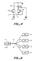
- FIG 4 shows one preferred embodiment of the switch MOD, the switch comprising first and second transistors 40, 41, a current source I M being connected to their common anodes, and their cathodes being connected to the laser LASC being modulated, as shown.
- transistor 41 is enabled so that the laser LASC is biased by the threshold current I B and the modulation current I M, and when a LOW pulse is to be generated by the laser LASC the transistor 41 is disabled so that the anode A of the laser is only connected to the pedestal current IB.
- FIGs 5A and 5B illustrate a detailed preferred electrical schematic of a circuit according to the invention.
- elements in FIG 5A and 5B which perform the functions referred to in FIG 3 are identified by identical reference symbols in each of these figures.
- a voltage converter 50 is provided for converting the TxD voltages from +5V and 0V to 0V and -5V respectively. These converted voltages are then inputted to the switch MOD which selectively connects the laser anode with the constant current I M as described during HIGH periods.
- An output B of the monitor laser is connected to the transimpedance amplifier 9 which is then connected to first and second feedback paths 32, 31 each having a comparator, flip-flop, and integrator, as previously described.
- Feedback loop 31 which includes the comparator 14, flip-flop 18, and integrator 22, controls the pedestal current I B , and the comparator 12, flip-flop 16, and integrator 20 of the feedback loop 32 control the modulation current IM.
- N equals the resistance of R96 divided by the resistance of R97.
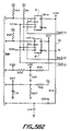
- FIG 6 illustrates a preferred use for the invention, this figure showing a host digital terminal 71 connected to a plurality of optical network units 72 via at least one optical fiber 73 which preferably transports bidirectional traffic.
- a splitter/combiner 74 splits a signal originating from the host digital terminal from the fiber 73 to a plurality of additional fibers 75 for transmission to each optical network unit, and conversely signals from each optical network unit 72 are combined at the point 74 so as to be transported to the host digital terminal via the fiber 73.
- high receiver sensitivity for each optical network unit is enhanced by maintaining an extinction ratio of a laser transmitting from the host digital terminal at a relatively high level, preferably above 10.
Landscapes
- Semiconductor Lasers (AREA)
- Optical Communication System (AREA)
Claims (12)
- Vorrichtung zum Steuern einer Laserlichtquelle (LASC) mit:einem Mittel (8,9) zum Detektieren einer ersten Spannungsgröße, welche die Intensität einer optischen Strahlung repräsentiert, die von der Laserlichtquelle (LASC) emittiert wird, während diese mit einem ersten Ausgangsleistungspegel (P1+P2) sendet, wobei der erste Ausgangsleistungspegel dem Senden einer logischen 1 entspricht;einem Mittel (12,16,20) zum Einstellen des ersten Ausgangsleistungspegels der Laserlichtquelle (LASC) zum Aufrechterhalten der ersten Spannungsgröße nahe an einem ersten voreingestellten Spannungswert (VR);einem Mittel (8,9,) zum Detektieren einer zweiten Spannungsgröße, welche die Intensität einer optischen Strahlung repräsentiert, die von der Laserlichtquelle (LASC) emittiert wird, während diese mit einem zweiten Ausgangsleistungspegel (P1) sendet, wobei der zweite Ausgangsleistungspegel dem Senden einer logischen 0 entspricht;einem Mittel (14,18,22) zum Einstellen des zweiten Ausgangsleistungspegels der Laserlichtquelle (LASC) zum Aufrechterhalten der zweiten Spannungsgröße nahe an einem zweiten voreingestellten Spannungswert (VR/N); undeinem Mittel (R96,R97) zum gleichzeitigen Einstellen des ersten und des zweiten voreingestellten Spannungswerts (VR; VR/N), während das Verhältnis aus dem ersten voreingestellten Wert (VR) und dem zweiten voreingestellten Wert (VR/N) konstant gehalten wird.
- Vorrichtung nach Anspruch 1, wobei die Laserlichtquelle (LASC) einen digital modulierbaren Laser aufweist, der optische Energie in wiederkehrenden Rahmen innerhalb eines im Zeitmultiplex betriebenen optischen Kommunikationsnetzwerks (71,72,73) emittiert.
- Vorrichtung nach Anspruch 1 oder 2, wobei das erste und das zweite Detektionsmittel (8,9) einen Strom-zu-Spannungs-Konverter (9) aufweisen, der einen Strom, welcher die von der Laserlichtquelle (LASC) ausgegebene optische Strahlung repräsentiert, in eine entsprechende Spannung konvertiert.
- Vorrichtung nach einem Ansprüche 1 bis 3, wobei das Mittel zum gleichzeitigen Einstellen des ersten und des zweiten voreingestellten Spannungswerts ein resistives Spannungsteilernetzwerk (R96,R97) aufweist.
- Vorrichtung nach einem der Ansprüche 1 bis 4, wobei das Mittel (12,16,20) zum Einstellen des ersten Ausgangsleistungspegels (P1+P2) einen ersten Komparator (12) zum Vergleichen der ersten Spannungsgröße mit dem ersten voreingestellten Spannungswert (VR), und ein Mittel (16,20) zum darauf antwortenden Einstellen eines Modulationsstroms (IM) der Laserlichtquelle (LASC) aufweist, um die erste Spannungsgröße nahe an dem ersten voreingestellten Wert (VR) aufrechtzuerhalten.
- Vorrichtung nach einem der Ansprüche 1 bis 5, wobei das Mittel (14,18,22) zum Einstellen des zweiten Ausgangsleistungspegels (P1) einen zweiten Komparator (14) zum Vergleichen der zweiten Spannungsgröße mit dem zweiten voreingestellten Spannungswert (VR/N), und ein Mittel (18,22) zum darauf antwortenden Einstellen eines Bias-Stroms (IB) der Laserlichtquelle aufweist, um die zweite Spannungsgröße nahe an dem zweiten voreingestellten Wert (VR/N) aufrechtzuerhalten.
- Vorrichtung nach Anspruch 6, wenn dieser auf Anspruch 5 zurückbezogen ist, ferner mit einem ersten und einem zweiten Flip-Flop (16,18) zum Stroben des ersten und des zweiten Komparators (12,14) zu solchen Zeitpunkten, die dem Senden von kontinuierlichen logischen 0- bzw. logischen 1-Signalen von der Laserlichtquelle (LASC) entsprechen.
- Vorrichtung nach Anspruch 7, wobei jedes von den kontinuierlichen logischen 1- und logischen 0-Signalen nicht-Daten-tragende Trainingsimpulse aufweist, von denen jedes wenigstens eine Länge von 6 Bit aufweist und in Auswahlrahmen eingebettet ist.
- Vorrichtung nach Anspruch 8, wobei die kontinuierliche logische 1 zum Erreichen eines stabilisierten, konstanten Werts für die detektierte erste Spannungsgröße ausreichend lange gesendet wird, und die kontinuierliche logische 0 zum Erreichen eines stabilisierten, konstanten Werts für die detektierte zweite Spannungsgröße ausreichend lange gesendet wird.
- Vorrichtung nach einem der Ansprüche 1 bis 9, wobei das erste und das zweite Detektionsmittel (8, 9) die erste und die zweite Spannungsgröße detektieren, und das erste und das zweite Einstellungsmittel (12, 16, 20; 14, 18, 22) den Modulations-bzw. den Bias-Strom (IM, IB) bei einer derart ausreichend hohen Frequenz einstellen, daß ein relativ konstantes Extinktionsverhältnis (N) der Laserlichtquelle (LASC) über Zeit und Temperatur aufrechterhalten wird.
- Vorrichtung nach einem der Ansprüche 1 bis 10, wobei das erste und das zweite Einstellungsmittel (12, 16, 20; 14, 18, 22) den Modulations- bzw. den Bias-Strom (IM; IB) erhöhen, wenn die erste und die zweite detektierte Spannungsgröße unterhalb dem ersten bzw. dem zweiten voreingestellten Spannungswert (VR; VR/N) sind, und den Modulations- und den Bias-Strom (IM; IB) verringern, wenn die erste und die zweite detektierte Spannungsgröße oberhalb des ersten bzw. des zweiten voreingestellten Spannungswerts (VR; VR/N) sind.
- Verfahren zum Einstellen der Ausgangsleistung einer Laserlichtquelle (LASC) mit den Schritten:Detektieren einer ersten Spannungsgröße, welche repräsentativ für die Intensität einer optischen Strahlung ist, die von dem Laser emittiert wird, während dieser mit einem H-Ausgangsleistungspegel (P1+P2) sendet, wobei der H-Ausgangsleistungspegel dem Senden einer logischen 1 entspricht;Einstellen des H-Ausgangsleistungspegels des Lasers, um die erste Spannungsgröße nahe an einem ersten voreingestellten Spannungswert (VR) aufrechtzuerhalten;Detektieren einer zweiten Spannungsgröße, welche repräsentativ für die Intensität einer optischen Strahlung ist, die von dem Laser emittiert wird, während dieser mit einem L-Ausgangsleistungspegel (P1) sendet, wobei der L-Ausgangsleistungspegel dem Senden einer logischen 0 entspricht;Einstellen des L-Ausgangsleistungspegels des Lasers, um die zweite Spannungsgröße nahe an einem zweiten voreingestellten Spannungswert (VR/N) aufrechtzuerhalten; undgleichzeitiges Einstellen des ersten und des zweiten voreingestellten Spannungswerts (VR; VR/N), während das Verhältnis (N) aus dem ersten voreingestellten Wert (VR) und dem zweiten voreingestellten Wert (VR/N) konstant aufrechterhalten wird, bis eine gewünschte Laserausgangsleistung erzielt wird.
Applications Claiming Priority (3)
| Application Number | Priority Date | Filing Date | Title |
|---|---|---|---|
| US81119791A | 1991-12-20 | 1991-12-20 | |
| US811197 | 1991-12-20 | ||
| PCT/US1992/011157 WO1993013577A1 (en) | 1991-12-20 | 1992-12-21 | Apparatus and method for controlling an extinction ratio of a laser diode over temperature |
Publications (2)
| Publication Number | Publication Date |
|---|---|
| EP0617852A1 EP0617852A1 (de) | 1994-10-05 |
| EP0617852B1 true EP0617852B1 (de) | 1998-02-25 |
Family
ID=25205850
Family Applications (1)
| Application Number | Title | Priority Date | Filing Date |
|---|---|---|---|
| EP93902712A Expired - Lifetime EP0617852B1 (de) | 1991-12-20 | 1992-12-21 | Vorrichtung und verfahren zur steuerung der temperaturabhängigkeit des ein/aus-verhältnisses einer laserdiode |
Country Status (6)
| Country | Link |
|---|---|
| EP (1) | EP0617852B1 (de) |
| JP (1) | JPH07502627A (de) |
| AT (1) | ATE163493T1 (de) |
| AU (1) | AU672188B2 (de) |
| CA (1) | CA2126323A1 (de) |
| DE (1) | DE69224534T2 (de) |
Families Citing this family (1)
| Publication number | Priority date | Publication date | Assignee | Title |
|---|---|---|---|---|
| US11454836B2 (en) * | 2018-06-29 | 2022-09-27 | Via Mechanics, Ltd. | Laser processing apparatus and laser processing method |
Family Cites Families (3)
| Publication number | Priority date | Publication date | Assignee | Title |
|---|---|---|---|---|
| US4995105A (en) * | 1989-09-18 | 1991-02-19 | Xerox Corporation | Adaptive laser diode driver circuit for laser scanners |
| US5091797A (en) * | 1989-11-13 | 1992-02-25 | Siemens Aktiengesellschaft | Method and apparatus for modulation current regulation for laser diodes |
| US5036189A (en) * | 1990-04-03 | 1991-07-30 | Raynet Corporation | Thermal control for laser diode used in outside plant communications terminal |
-
1992
- 1992-12-21 AU AU34186/93A patent/AU672188B2/en not_active Ceased
- 1992-12-21 JP JP5511863A patent/JPH07502627A/ja active Pending
- 1992-12-21 AT AT93902712T patent/ATE163493T1/de not_active IP Right Cessation
- 1992-12-21 CA CA 2126323 patent/CA2126323A1/en not_active Abandoned
- 1992-12-21 DE DE69224534T patent/DE69224534T2/de not_active Expired - Lifetime
- 1992-12-21 EP EP93902712A patent/EP0617852B1/de not_active Expired - Lifetime
Also Published As
| Publication number | Publication date |
|---|---|
| DE69224534T2 (de) | 1998-09-17 |
| ATE163493T1 (de) | 1998-03-15 |
| CA2126323A1 (en) | 1993-07-08 |
| AU3418693A (en) | 1993-07-28 |
| EP0617852A1 (de) | 1994-10-05 |
| JPH07502627A (ja) | 1995-03-16 |
| DE69224534D1 (de) | 1998-04-02 |
| AU672188B2 (en) | 1996-09-26 |
Similar Documents
| Publication | Publication Date | Title |
|---|---|---|
| US5502298A (en) | Apparatus and method for controlling an extinction ratio of a laser diode over temperature | |
| US7519093B2 (en) | Laser driver circuit and system | |
| EP0574816B1 (de) | Laservorspannungs- und -modulationsschaltung | |
| CA2073430C (en) | Laser control circuit | |
| EP0539038B1 (de) | Optische Sender | |
| GB1563944A (en) | Imjection lasers | |
| EP0878882B1 (de) | Stromsteuerung für eine analoge optische Verbindung | |
| US6907055B2 (en) | Method and circuit for measuring the optical modulation amplitude (OMA) in the operating region of a laser diode | |
| US20020093714A1 (en) | Optical transmitter and optical transmitting apparatus using the same | |
| US7245828B2 (en) | Extinction ratio determination using duty cycle modulation | |
| US4876442A (en) | Laser control circuit | |
| WO1993013577A1 (en) | Apparatus and method for controlling an extinction ratio of a laser diode over temperature | |
| US5091797A (en) | Method and apparatus for modulation current regulation for laser diodes | |
| US20030067947A1 (en) | Laser control circuit for maintaining constant power and extinction ratio | |
| AU672188B2 (en) | Apparatus and method for controlling an extinction ratio of a laser diode over temperature | |
| JP2001251254A (ja) | 光送信器及び光伝送システム | |
| JP2842369B2 (ja) | レーザダイオード駆動回路 | |
| US20020163945A1 (en) | Modulation current compensation of laser for controlled extinction ratio using dither signal | |
| US7590351B2 (en) | Extinction ratio control using a frequency spread tone to modulate optical signal power levels | |
| CN117061009B (zh) | 光通信发射机激光驱动器的光调制幅度控制方法及架构 | |
| JPH0324831A (ja) | レーザダイオード駆動方法および装置 | |
| JP2626470B2 (ja) | デジタル光通信における光出力制御装置 | |
| JPH04304689A (ja) | 光送信器 | |
| WO1992017007A1 (en) | Method and control circuit for controlling a laser diode transmitter | |
| JPH0553078B2 (de) |
Legal Events
| Date | Code | Title | Description |
|---|---|---|---|
| PUAI | Public reference made under article 153(3) epc to a published international application that has entered the european phase |
Free format text: ORIGINAL CODE: 0009012 |
|
| 17P | Request for examination filed |
Effective date: 19940525 |
|
| AK | Designated contracting states |
Kind code of ref document: A1 Designated state(s): AT BE CH DE DK ES FR GB GR IE IT LI NL PT SE |
|
| 17Q | First examination report despatched |
Effective date: 19951222 |
|
| GRAG | Despatch of communication of intention to grant |
Free format text: ORIGINAL CODE: EPIDOS AGRA |
|
| GRAG | Despatch of communication of intention to grant |
Free format text: ORIGINAL CODE: EPIDOS AGRA |
|
| GRAH | Despatch of communication of intention to grant a patent |
Free format text: ORIGINAL CODE: EPIDOS IGRA |
|
| RAP1 | Party data changed (applicant data changed or rights of an application transferred) |
Owner name: ERICSSON RAYNET, A DELAWARE GENERAL PARTNERSHIP |
|
| GRAH | Despatch of communication of intention to grant a patent |
Free format text: ORIGINAL CODE: EPIDOS IGRA |
|
| GRAA | (expected) grant |
Free format text: ORIGINAL CODE: 0009210 |
|
| AK | Designated contracting states |
Kind code of ref document: B1 Designated state(s): AT BE CH DE DK ES FR GB GR IE IT LI NL PT SE |
|
| PG25 | Lapsed in a contracting state [announced via postgrant information from national office to epo] |
Ref country code: NL Free format text: LAPSE BECAUSE OF FAILURE TO SUBMIT A TRANSLATION OF THE DESCRIPTION OR TO PAY THE FEE WITHIN THE PRESCRIBED TIME-LIMIT Effective date: 19980225 Ref country code: LI Free format text: LAPSE BECAUSE OF FAILURE TO SUBMIT A TRANSLATION OF THE DESCRIPTION OR TO PAY THE FEE WITHIN THE PRESCRIBED TIME-LIMIT Effective date: 19980225 Ref country code: IT Free format text: LAPSE BECAUSE OF FAILURE TO SUBMIT A TRANSLATION OF THE DESCRIPTION OR TO PAY THE FEE WITHIN THE PRE;WARNING: LAPSES OF ITALIAN PATENTS WITH EFFECTIVE DATE BEFORE 2007 MAY HAVE OCCURRED AT ANY TIME BEFORE 2007. THE CORRECT EFFECTIVE DATE MAY BE DIFFERENT FROM THE ONE RECORDED.SCRIBED TIME-LIMIT Effective date: 19980225 Ref country code: GR Free format text: LAPSE BECAUSE OF NON-PAYMENT OF DUE FEES Effective date: 19980225 Ref country code: FR Free format text: LAPSE BECAUSE OF FAILURE TO SUBMIT A TRANSLATION OF THE DESCRIPTION OR TO PAY THE FEE WITHIN THE PRESCRIBED TIME-LIMIT Effective date: 19980225 Ref country code: ES Free format text: THE PATENT HAS BEEN ANNULLED BY A DECISION OF A NATIONAL AUTHORITY Effective date: 19980225 Ref country code: CH Free format text: LAPSE BECAUSE OF FAILURE TO SUBMIT A TRANSLATION OF THE DESCRIPTION OR TO PAY THE FEE WITHIN THE PRESCRIBED TIME-LIMIT Effective date: 19980225 Ref country code: BE Free format text: LAPSE BECAUSE OF FAILURE TO SUBMIT A TRANSLATION OF THE DESCRIPTION OR TO PAY THE FEE WITHIN THE PRESCRIBED TIME-LIMIT Effective date: 19980225 Ref country code: AT Free format text: LAPSE BECAUSE OF FAILURE TO SUBMIT A TRANSLATION OF THE DESCRIPTION OR TO PAY THE FEE WITHIN THE PRESCRIBED TIME-LIMIT Effective date: 19980225 |
|
| REF | Corresponds to: |
Ref document number: 163493 Country of ref document: AT Date of ref document: 19980315 Kind code of ref document: T |
|
| REG | Reference to a national code |
Ref country code: CH Ref legal event code: EP |
|
| REF | Corresponds to: |
Ref document number: 69224534 Country of ref document: DE Date of ref document: 19980402 |
|
| PG25 | Lapsed in a contracting state [announced via postgrant information from national office to epo] |
Ref country code: SE Free format text: LAPSE BECAUSE OF FAILURE TO SUBMIT A TRANSLATION OF THE DESCRIPTION OR TO PAY THE FEE WITHIN THE PRESCRIBED TIME-LIMIT Effective date: 19980525 Ref country code: PT Free format text: LAPSE BECAUSE OF FAILURE TO SUBMIT A TRANSLATION OF THE DESCRIPTION OR TO PAY THE FEE WITHIN THE PRESCRIBED TIME-LIMIT Effective date: 19980525 Ref country code: DK Free format text: LAPSE BECAUSE OF FAILURE TO SUBMIT A TRANSLATION OF THE DESCRIPTION OR TO PAY THE FEE WITHIN THE PRESCRIBED TIME-LIMIT Effective date: 19980525 |
|
| REG | Reference to a national code |
Ref country code: IE Ref legal event code: FG4D Free format text: 78978 |
|
| EN | Fr: translation not filed | ||
| NLV1 | Nl: lapsed or annulled due to failure to fulfill the requirements of art. 29p and 29m of the patents act | ||
| REG | Reference to a national code |
Ref country code: CH Ref legal event code: PL |
|
| PGFP | Annual fee paid to national office [announced via postgrant information from national office to epo] |
Ref country code: DK Payment date: 19981207 Year of fee payment: 7 Ref country code: IE Payment date: 19981207 Year of fee payment: 7 |
|
| PLBE | No opposition filed within time limit |
Free format text: ORIGINAL CODE: 0009261 |
|
| STAA | Information on the status of an ep patent application or granted ep patent |
Free format text: STATUS: NO OPPOSITION FILED WITHIN TIME LIMIT |
|
| 26N | No opposition filed | ||
| PGFP | Annual fee paid to national office [announced via postgrant information from national office to epo] |
Ref country code: GB Payment date: 19991203 Year of fee payment: 8 |
|
| PG25 | Lapsed in a contracting state [announced via postgrant information from national office to epo] |
Ref country code: IE Free format text: LAPSE BECAUSE OF NON-PAYMENT OF DUE FEES Effective date: 19991221 |
|
| REG | Reference to a national code |
Ref country code: IE Ref legal event code: MM4A |
|
| PG25 | Lapsed in a contracting state [announced via postgrant information from national office to epo] |
Ref country code: GB Free format text: LAPSE BECAUSE OF NON-PAYMENT OF DUE FEES Effective date: 20001221 |
|
| GBPC | Gb: european patent ceased through non-payment of renewal fee |
Effective date: 20001221 |
|
| PGFP | Annual fee paid to national office [announced via postgrant information from national office to epo] |
Ref country code: DE Payment date: 20111229 Year of fee payment: 20 |
|
| REG | Reference to a national code |
Ref country code: DE Ref legal event code: R071 Ref document number: 69224534 Country of ref document: DE |