EP0616272B1 - Circuit for suppressing the bouncing effects during closing and opening of a contact in a watch - Google Patents
Circuit for suppressing the bouncing effects during closing and opening of a contact in a watch Download PDFInfo
- Publication number
- EP0616272B1 EP0616272B1 EP94103849A EP94103849A EP0616272B1 EP 0616272 B1 EP0616272 B1 EP 0616272B1 EP 94103849 A EP94103849 A EP 94103849A EP 94103849 A EP94103849 A EP 94103849A EP 0616272 B1 EP0616272 B1 EP 0616272B1
- Authority
- EP
- European Patent Office
- Prior art keywords
- signal
- contactor
- time
- circuit
- sampling
- Prior art date
- Legal status (The legal status is an assumption and is not a legal conclusion. Google has not performed a legal analysis and makes no representation as to the accuracy of the status listed.)
- Expired - Lifetime
Links
Images

Classifications
-
- G—PHYSICS
- G04—HOROLOGY
- G04C—ELECTROMECHANICAL CLOCKS OR WATCHES
- G04C3/00—Electromechanical clocks or watches independent of other time-pieces and in which the movement is maintained by electric means
- G04C3/14—Electromechanical clocks or watches independent of other time-pieces and in which the movement is maintained by electric means incorporating a stepping motor
-
- G—PHYSICS
- G04—HOROLOGY
- G04C—ELECTROMECHANICAL CLOCKS OR WATCHES
- G04C3/00—Electromechanical clocks or watches independent of other time-pieces and in which the movement is maintained by electric means
- G04C3/001—Electromechanical switches for setting or display
- G04C3/007—Electromechanical contact-making and breaking devices acting as pulse generators for setting
Description
La présente invention concerne des circuits pour supprimer les effets de rebonds et les commutations parasites d'un contacteur et pour fournir un signal bien défini représentatif de la position ouverte ou fermée du contacteur (EP-A-0 274 035). L'invention convient pour une utilisation dans des montres électroniques analogiques.The present invention relates to circuits for suppressing rebound effects and parasitic switching of a contactor and for providing a well-defined signal representative of the open or closed position of the contactor (EP-A-0 274 035). The invention is suitable for use in analog electronic watches.
De nombreux contacteurs mécaniques sont incapables de commuter d'une position ouverte à une position fermée sans rebonds. De plus, on sait que des commutations parasites peuvent également se produire, sous l'effet soit d'un choc soit d'une réduction temporaire de la force qui maintient le contacteur dans une de ces deux positions. De tels rebonds ou commutations parasites affectent naturellement de façon néfaste la qualité du signal produit par le contacteur.Many mechanical contactors are unable to switch from an open position to a closed position without rebounds. In addition, it is known that parasitic commutations can also occur, under the effect of either an impact or a temporary reduction in the force which keeps the contactor in one of these two positions. Such bounces or spurious switching naturally adversely affect the quality of the signal produced by the contactor.
Certains contacteurs utilisés dans les montres présentent les inconvénients qui viennent d'être décrits. Un tel problème se présente par exemple avec des montres électroniques analogiques comprenant un calendrier périphérique dont le circuit est prévu pour recevoir un signal bi-journalier produit par le contacteur. Ce contacteur, généralement constitué par une paire de lames flexibles, est activé deux fois par jour par une came disposée sur le canon des heures. En fonctionnement normal, le temps de commutation entre l'instant où les lames se touchent pour la première fois et l'instant où elles sont fermement en contact l'une avec l'autre est de l'ordre d'une à deux minutes. Le contacteur demeure ensuite fermé pendant idéalement environ trente minutes avant que les lames ne commencent à s'écarter à nouveau. Le temps de commutation entre l'instant où les lames commencent à s'écarter et l'instant où elles sont complètement séparées l'une de l'autre, est d'une à deux minutes.Certain contactors used in watches have the disadvantages which have just been described. Such a problem arises for example with analog electronic watches comprising a peripheral calendar whose circuit is designed to receive a bi-daily signal produced by the contactor. This contactor, generally consisting of a pair of flexible blades, is activated twice a day by a cam placed on the hour barrel. In normal operation, the switching time between the moment when the blades touch for the first time and the moment when they are firmly in contact with each other is of the order of one to two minutes. The contactor then remains closed for ideally about thirty minutes before the blades start to move apart again. The switching time between the moment when the blades start to move apart and the moment when they are completely separated from each other, is one to two minutes.
Pour économiser de la place et réduire le couple sur la came, on utilise de préférence des lames flexibles qui ont une course réduite et qui nécessitent seulement l'application d'une force limitée aussi bien pour produire le déplacement des lames que pour les maintenir fermement en contact l'une avec l'autre. Ceci rend le contacteur particulièrement sensible aux chocs qui peuvent produire des ouvertures où des fermetures accidentelles du contacteur. De plus, des erreurs minimes dans les tolérances pour la came ou pour les lames de contact, ou encore d'autres problèmes d'alignement mécanique peuvent rendre la force exercée par la came sur les lames de contact temporairement insuffisante pour maintenir les lames fermement en contact l'une avec l'autre. Il se peut également que les lames, lors de leur séparation, ne se détachent pas complètement l'une de l'autre et qu'une conductivité faible subsiste entre celles-ci (cette situation sera ci-après appelée un mauvais contact). Des erreurs comme celles qui ont été mentionnées plus haut peuvent également entraîner des variations dans le temps de commutation des lames de contact.To save space and reduce the torque on the cam, flexible blades are preferably used which have a reduced stroke and which only require the application of a limited force both to produce the displacement of the blades and to hold them firmly in contact with each other. This makes the contactor particularly sensitive to shocks which can produce openings or accidental closings of the contactor. In addition, small errors in tolerances for the cam or for the contact blades, or other mechanical alignment problems can make the force exerted by the cam on the contact blades temporarily insufficient to keep the blades firmly in place. contact with each other. It is also possible that the blades, when they separate, do not completely detach from each other and that a low conductivity remains between them (this situation will hereinafter be called poor contact). Errors such as those mentioned above can also lead to variations in the switching time of the contact blades.
On connaît des circuits destinés à remédier au moins partiellement aux problèmes susmentionnés, de tels circuits sont appelés des circuits anti-rebonds (JP-A-55 075 351). Un exemple particulier d'un tel circuit comprend un monostable dont la sortie fournit un signal d'une durée déterminée en réponse à une première ouverture ou fermeture du contacteur. Grâce à cette construction, les rebonds du contacteur qui se produisent immédiatement après le premier signal fourni par le contacteur n'ont pas d'effet sur le signal, pour autant que la durée prédéterminée de celui-ci soit plus grande que le temps de commutation du contacteur. Ce type de circuit convient pour des applications dans lesquelles il est associé avec un contacteur qui a un temps de commutation sensiblement constant, dans lequel les lames de contact restent fermement en contact l'une avec l'autre durant le fonctionnement du contacteur, et qui n'est pas sensible aux chocs extérieurs. Toutefois, dans d'autres applications un tel circuit peut produire des signaux parasites.Circuits are known which are intended to at least partially remedy the aforementioned problems, such circuits are called anti-rebound circuits (JP-A-55,075,351). A particular example of such a circuit comprises a monostable whose output provides a signal of a determined duration in response to a first opening or closing of the contactor. Thanks to this construction, the bounces of the contactor which occur immediately after the first signal provided by the contactor have no effect on the signal, provided that the predetermined duration of the latter is greater than the time of contactor switching. This type of circuit is suitable for applications in which it is associated with a contactor which has a substantially constant switching time, in which the contact blades remain firmly in contact with each other during the operation of the contactor, and which is not sensitive to external shocks. However, in other applications such a circuit can produce spurious signals.
En particulier, si par exemple le temps de commutation du contacteur varie et dépasse la durée du signal fourni par le monostable, les rebonds produiront encore un ou plusieurs signaux parasites. De tels signaux parasites seront également générés par le circuit lorsque le contacteur se déplace entre l'une et l'autre de ces positions alors qu'il est au repos, comme cela peut être le cas lors d'un choc accidentel d'une violence suffisante. En outre, les problèmes qui pourraient être causés par la présence d'un ou de plusieurs mauvais contacts durant le temps idéal de fermeture du contacteur ne sont pas non plus résolus par ce circuit.In particular, if for example the switching time of the contactor varies and exceeds the duration of the signal supplied by the monostable, the rebounds will still produce one or more parasitic signals. Such parasitic signals will also be generated by the circuit when the contactor moves between one and the other of these positions while it is at rest, as can be the case during an accidental shock of violence. sufficient. In addition, problems that could be caused by the presence of one or more bad contacts during the ideal contactor closing time are also not solved by this circuit.
Un autre circuit, qui est moins sensible aux perturbations causées par les chocs extérieurs est décrit dans la demande de brevet suisse CH-D-4130/74. Ce circuit comprend essentiellement un compteur, pouvant compter jusqu'à N, et qui, lorsqu'il est rempli, fournit un signal en sortie. En plus, ce circuit comprend un générateur fournissant un signal de fréquence fixe formé d'une succession d'impulsions. Lorsque le contacteur est fermé, les impulsions sont fournies au compteur, alors que lorsque le contacteur est ouvert, la succession des impulsions est interrompue et le compteur est remis à zéro.Another circuit, which is less sensitive to disturbances caused by external shocks, is described in Swiss patent application CH-D-4130/74. This circuit essentially comprises a counter, which can count up to N, and which, when filled, provides an output signal. In addition, this circuit includes a generator providing a fixed frequency signal formed by a succession of pulses. When the contactor is closed, the pulses are supplied to the counter, while when the contactor is open, the succession of pulses is interrupted and the counter is reset to zero.
Lors de la fermeture du contacteur d'un tel circuit, le compteur est remis à zéro chaque fois que le contacteur s'ouvre en raison de chocs ou de rebonds. La fréquence des impulsions et le nombre N sont de plus choisis de façon que, durant cette période d'instabilité du contacteur, le compteur n'ait pas le temps de recevoir N impulsions consécutives. Ce n'est qu'après le dernier rebond, une fois que le contacteur est fermé suffisamment fermement pour qu'il ne soit plus sensible aux chocs et aux rebonds, que le compteur, ayant enfin reçu N impulsions consécutives, fournit un signal représentatif de l'état fermé du contacteur. Signalons toutefois que les ouvertures répétées des lames de contact en raison de chocs ou de mauvais contacts remettront continuellement à zéro le compteur de sorte que le signal de fermeture risque de ne jamais être fourni.When the contactor of such a circuit is closed, the counter is reset to zero each time the contactor opens due to shocks or rebounds. The frequency of pulses and the number N are also chosen so that, during this period of contactor instability, the counter does not have time to receive N consecutive pulses. It is only after the last rebound, once the contactor is closed firmly enough that it is no longer sensitive to shocks and rebounds, that the counter, having finally received N consecutive pulses, provides a signal representative of the closed state of the contactor. Note however that repeated opening of the contact blades due to shocks or bad contacts will continuously reset the counter so that the closing signal may never be provided.
Un autre circuit connu, comprenant un deuxième compteur et un deuxième générateur d'impulsions, peut être utilisé pour supprimer les effets des ouvertures indésirées des lames de contact. Par exemple, un tel circuit peut être conçu de façon qu'après l'émission d'un signal indiquant la fermeture du contacteur, lorsque les lames de contact se séparent à nouveau, elles doivent rester ouvertes durant N impulsions consécutives avant que le circuit n'interprète l'état du contacteur comme étant ouvert. Ce circuit peut, en principe, ainsi éliminer les effets d'ouverture brève des lames de contact dus à des chocs produits après l'émission du signal de fermeture.Another known circuit, comprising a second counter and a second pulse generator, can be used to suppress the effects of unwanted openings of the contact blades. For example, such a circuit can be designed so that after the emission of a signal indicating the closure of the contactor, when the contact blades separate again, they must remain open for N consecutive pulses before the circuit n 'interprets the state of the contactor as being open. This circuit can, in principle, thus eliminate the effects of brief opening of the contact blades due to shocks produced after the emission of the closing signal.
Toutefois, un mauvais contact peut se produire durant le temps pendant lequel le contacteur est en principe fermé, et durer plus longtemps que les ouvertures brèves produites par les chocs. Si les lames de contact sont ouvertes durant une période suffisamment longue pour que le deuxième compteur reçoive N impulsions successives, ce circuit interprétera cela comme un signal indiquant que le contacteur est ouvert. Si, par la suite, les lames du contacteur se ferment à nouveau pour une période suffisamment longue pour que le premier compteur reçoive N impulsions consécutives, un deuxième signal parasite indiquant que le contacteur s'est à nouveau fermé sera fourni.However, poor contact can occur during the time that the contactor is normally closed, and last longer than the brief openings produced by the shocks. If the contact blades are open for a period long enough for the second counter to receive N successive pulses, this circuit will interpret this as a signal that the contactor is open. If, subsequently, the contactor blades close again for a period long enough for the first counter to receive N consecutive pulses, a second parasitic signal indicating that the contactor has closed again will be provided.
Un but de la présente invention est de fournir un circuit pour supprimer les effets de rebonds et les commutations parasites d'un contacteur, qui remédie aux inconvénients des contacteurs anti-rebonds connus.An object of the present invention is to provide a circuit for suppressing the effects of rebounds and parasitic switching of a contactor, which overcomes the drawbacks of known anti-rebound contactors.
Ainsi, la présente invention fournit un circuit pour supprimer les effets des rebonds et des commutations parasites d'un contacteur sur un signal de commande produit par le contacteur, ledit signal de commande étant soit dans un premier état correspondant à la position ouverte dudit contacteur, soit dans un second état correspondant à la position fermée dudit contacteur, ledit contacteur étant destiné à passer d'une desdites positions à l'autre desdites positions et à rester dans ladite autre position durant un temps prédéterminé, caractérisé en ce que ledit circuit comprend des moyens d'échantillonnage pour échantillonner ledit signal de commande à une première fréquence d'échantillonnage et fournissant un signal de sortie se trouvant soit dans ledit premier état soit dans ledit second état, des moyens de détection pour déterminer un changement dudit signal de sortie entre un desdits états et l'autre état, et des moyens de blocage de l'échantillonnage pour empêcher lesdits moyens d'échantillonnage d'échantillonner ledit signal de commande pour la durée dudit temps prédéterminé en réponse au changement dans l'état dudit signal de sortie, pour que ledit signal de sortie reste dans ledit autre état pendant ladite durée au moins.Thus, the present invention provides a circuit for suppressing the effects of rebounds and parasitic switching of a contactor on a control signal produced by the contactor, said control signal being either in a first state corresponding to the open position of said contactor, either in a second state corresponding to the closed position of said contactor, said contactor being intended to pass from one of said positions to the other of said positions and to remain in said other position for a predetermined time, characterized in that said circuit comprises sampling means for sampling said control signal at a first sampling frequency and providing an output signal being either in said first state or in said second state, detection means for determining a change in said output signal between a of said states and the other state, and means for blocking sampling for r preventing said sampling means from sampling said control signal for the duration of said predetermined time in response to the change in the state of said output signal, so that said output signal remains in said other state for at least said duration.
Ainsi, un signal bien défini représentatif de la position du contacteur est fourni qui a un état qui demeure constant au moins pour la durée du temps de fermeture théorique du contacteur, et dont l'état n'est pas affecté par les ouvertures et les fermetures des lames de contact dues à des chocs ou à des mauvais contacts durant ce temps de fermeture théorique.Thus, a well-defined signal representative of the position of the contactor is provided which has a state which remains constant at least for the duration of the theoretical closing time of the contactor, and whose state is not affected by the openings and closings. contact blades due to shocks or poor contacts during this theoretical closing time.
La description qui va suivre se réfère en plus de détail à diverses caractéristiques du circuit pour supprimer les effets de rebonds et les commutations parasites d'un contacteur selon la présente invention. De façon à faciliter la compréhension de l'invention, on fera référence dans la description aux dessins annexés qui illustrent un mode de réalisation préféré de l'invention. L'homme du métier comprendra que le circuit de la présente invention ne se limite pas au mode de réalisation préféré illustré sur les figures, dans lesquelles :
- la figure 1 est un schéma bloc d'un mode de réalisation du circuit conforme à la présente invention;
- la figure 2 est le schéma d'un circuit correspondant au mode de réalisation du schéma bloc de la figure 1; et
- la figure 3 décrit, sous forme de graphique, l'évolution au cours du temps des différents signaux produits dans le circuit représenté à la figure 2.
- Figure 1 is a block diagram of an embodiment of the circuit according to the present invention;
- Figure 2 is a diagram of a circuit corresponding to the embodiment of the block diagram of Figure 1; and
- FIG. 3 describes, in the form of a graph, the evolution over time of the different signals produced in the circuit represented in FIG. 2.
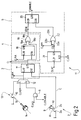
En se reportant maintenant à la figure 1, on voit que le circuit 1, selon la présente invention, comporte un contacteur mécanique 2, un circuit d'échantillonnage 3, un détecteur de changement d'état 4 et un circuit d'évaluation du temps 5. Le contacteur mécanique 2 comprend un lame fixe 2a et une lame mobile 2b qui, au repos, ne se touchent pas. Le contacteur 2 est actionné par une came 8 qui est entraînée en rotation dans un seul sens (référencé 9) par un arbre. La came comporte encore un doigt 10 qui, durant son déplacement, actionne la lame 2b pour que celle-ci entre en contact avec la lame 2a et provoque la fermeture du contacteur.Referring now to FIG. 1, it can be seen that the
La lame 2a est reliée à la borne positive d'une alimentation, de manière que, lorsque le contacteur 2 est dans sa position fermée, un signal logique C de niveau haut soit fourni au circuit d'échantillonnage 3. Inversement, lorsque le contacteur 2 est dans sa position ouverte, le signal C est à un niveau logique bas.The
Le circuit d'échantillonnage 3 échantillonne le signal C avec une fréquence qui est déterminée par un signal d'horloge CLKA, et fournit en sortie un signal de sortie Ci dont le niveau logique correspond au niveau logique du signal C à l'instant de l'échantillonnage. Ce signal Ci est reçu par l'entrée du détecteur de changement d'état 4.The
Lorsque l'état du signal Ci demeure constant, le détecteur 4 fournit un signal de niveau logique bas au circuit d'évaluation du temps 5. Dans ces conditions, le circuit d'évaluation du temps 5 fournit un signal logique de niveau haut à l'une des entrées d'une porte ET 6. Le signal d'horloge CLKA est fournit à l'autre entrée de la porte ET 6, de manière que le signal C soit échantillonné par le circuit d'échantillonnage 3 à une fréquence déterminée par le signal d'horloge CLKA.When the state of the signal C i remains constant, the
La détection d'un changement dans l'état du signal Ci provoque l'émission, par le détecteur 4, d'un signal logique de niveau haut vers le circuit d'évaluation du temps 5. Lorsque le circuit d'évaluation du temps 5 détecte ce signal logique de niveau haut, un signal logique de niveau bas est fourni à l'une des entrées de la porte ET 6, de manière à empêcher la transmission des impulsions d'horloge CLKA vers le circuit d'échantillonnage 3 et ainsi de bloquer l'échantillonnage du signal C.The detection of a change in the state of the signal C i causes the
Le circuit d'évaluation du temps 5 fournit ce signal logique de niveau bas à l'entrée de la porte ET 6 pendant un laps de temps égal au temps de fermeture théorique du contacteur 2. Ce laps de temps peut, par exemple, être déterminé par un compteur intégré dans le circuit d'évaluation du temps 5. Ce compteur commence à compter à l'instant où le signal logique haut produit par le détecteur 4 est initialement détecté et est incrémenté avec une fréquence déterminée par un signal d'horloge CLKM. A la fin de ce laps de temps prédéterminé, le circuit d'évaluation du temps 5 fournit à nouveau un signal logique de niveau haut à ladite entrée de la porte ET 6, de manière à permettre la transmission d'impulsions fournies par le signal de base de temps CLKA au circuit d'échantillonnage 3 pour permettre la reprise de l'échantillonnage du signal C. L'état du signal Ci est donc maintenu constant durant la période de fermeture théorique et le signal n'est pas affecté par les ouvertures accidentelles des lames de contact 2a et 2b produites par exemple par des chocs ou des mauvais contacts.The
On va maintenant se référer à la figure 2 qui représente un mode particulier de réalisation du circuit de la présente invention conforme au schéma bloc de la figure 1, et nous ferons simultanément référence aux graphiques de l'évolution des signaux au cours du temps représentés à la figure 3. La figure 2 représente un circuit 11 comprenant le contacteur mécanique 2, le circuit d'échantillonnage 3, le détecteur de changement d'état 4, le circuit d'évaluation de temps 5 et la porte ET 6 déjà décrite en référence à la figure 1. Le circuit 11 comprend également un multiplexeur 12 et un deuxième contacteur mécanique 13 actionné par une couronne 14.We will now refer to FIG. 2 which represents a particular embodiment of the circuit of the present invention in accordance with the block diagram of FIG. 1, and we will simultaneously refer to the graphs of the evolution of the signals over time represented at FIG. 3. FIG. 2 represents a
Le contacteur 13 comprend une lame fixe 15 et une lame mobile 16 qui, au repos, ne se touchent pas. Les lames de contact 15 et 16 sont amenées en contact l'une avec l'autre lorsque la couronne 14 est placée dans sa position de mise à l'heure, et retournent dans leur position ouverte lorsque la couronne 14 est remise dans sa position de fonctionnement normal. La lame 15 est reliée à la borne positive d'une source de tension, de manière que lorsque le contacteur 13 est dans sa position fermée, un signal logique de niveau haut soit envoyé au multiplexeur 12, et que lorsque le contacteur 13 est dans sa position ouverte, le signal envoyé soit de niveau logique bas.The
Le circuit d'échantillonnage 3 comprend un bascule de type D référencée 17 dont l'entrée D17 est reliée à la lame de contact 7 du contacteur 2. La bascule 17 a son entrée de base de temps CL17 reliée à la sortie du miltiplexeur 12. Dans ces conditions, c'est donc le signal fourni par le multiplexeur 12 qui détermine la fréquence avec laquelle le signal fournit à l'entrée D17 de la bascule 17 est échantillonné. Un signal d'horloge CLKB est relié à l'une des entrées I1 du multiplexeur 12. Un autre signal d'horloge qui est produit par la combinaison au niveau de la porte ET 6 du signal d'horloge CLKA et du signal de commande d'échantillonnage CLENABLE est fourni à l'autre entrée I2 du multiplexeur 12. Lorsque le contacteur 13 est fermé, le signal logique de niveau haut émis par le multiplexeur provoque la transmission du signal d'horloge reçu par l'entrée I1 vers le circuit d'échantillonnage 3. Inversement, lorsque le contacteur 13 est ouvert, le signal reçu par l'entrée I2 est envoyé au circuit d'échantillonnage 3.The
Le détecteur de changement d'état 4 comprend une autre bascule de type D référencée 18 et une porte ou-exclusif (XOR) 19. La bascule 18 est reliée par son entrée D18 à la sortie Q17 de la bascule 17, et son entrée d'horloge CL18 est alimentée par le signal d'horloge CLKA. La sortie Q18 de la bascule 18 est reliée à l'une des entrées 19a de la porte XOR 19. L'autre entrée 19b de la porte XOR 19 est reliée à l'entrée D18 de la bascule 18.The
Lorsque, durant plusieurs cycles consécutifs, l'état du signal à l'entrée D18 de la bascule 18 reste inchangé, l'entrée D18 et la sortie Q18 de la bascule 18 seront toutes deux dans le même état logique. La porte XOR 19 fournira donc un signal logique de niveau bas à sa sortie 19c. Toutefois, lorsque le signal à l'entrée D18 de la bascule 17 change entre deux cycles consécutifs du signal de base de temps CLKA, et passe d'un niveau logique haut à un niveau logique bas (ou vice versa), la sortie 19c enverra, durant l'un des cycles du signal de base de temps CLKA, une impulsion logique de niveau haut au circuit d'évaluation du temps 5.When, during several consecutive cycles, the state of the signal at the input D18 of the flip-
Le circuit d'évaluation du temps 5 comprend une bascule RS 20, un compteur 21 et une porte OU 22. La bascule RS 20 a son entrée de reset R20 reliée à la sortie 19c de la porte XOR 19, de manière à ce que l'impulsion de niveau logique haut émise par le détecteur 4 produise un reset de la bascule RS 20 et provoque le passage de la sortie Q20 à un niveau logique bas. Le signal CLENABLE est produit par la sortie Q20.The
Le compteur 21 a une entrée de reset R21 qui, lorsqu'un signal logique de niveau haut lui est fourni, remet le compteur 21 à zéro. Une entrée de base de temps CL21 est en outre prévue pour déterminer la fréquence avec laquelle le compteur 21 s'incrémente lorsqu'il est en fonction. Le compteur 21 comprend également une sortie Q21 qui fournit un signal logique de niveau haut à une entrée 22a de la porte OU 22 lorsque le compteur 21 a été incrémenté d'un nombre déterminé d'unités. La sortie du multiplexeur 12 fournit un signal de base de temps CLKM à l'autre entrée 22b de la porte OU 22 et à l'entrée de reset 21 du compteur 21. Lorsque soit la sortie Q21 soit le signal de base de temps CLKM passe à un niveau haut, un signal de niveau logique haut est émis par la sortie 22c de la porte OU 22 vers l'entrée S20 de la bascule RS 20, ce qui entraîne le passage du signal CLENABLE fourni par la sortie Q20 à un état logique haut.
Le fonctionnement du circuit 11 lors de la remise à l'heure sera maintenant décrit. Lorsque la couronne 14 est placée dans sa position de mise à l'heure, le contacteur 13 se ferme et un signal logique de niveau haut est émis vers le multiplexeur. Le signal d'horloge CLKB est ainsi fourni par la sortie du multiplexeur 12 à l'entrée de base de temps CL17 de la bascule 17. Dans cette position, la couronne 14 peut être tournée dans une direction pour provoquer la rotation de la came 8 dans le sens 9.The operation of
Conformément à ce qui a été expliqué ci-dessus, dans le mode de fonctionnement normal, la came 8 tourne suffisamment lentement pour que le contacteur 8 reste idéalement fermé pendant une durée de l'ordre de 30 minutes. Toutefois, dans le mode de mise à l'heure, la rotation de la came est commandée par la couronne 14 et peut donc être beaucoup plus rapide. Puisque dans ces conditions il est nécessaire d'avoir une grande fréquence d'échantillonnage pour échantillonner le signal C produit par le contacteur 2, le signal d'horloge CLKB, qui détermine cette fréquence d'échantillonnage, doit être de fréquence élevée, et peut être de l'ordre de 500 échantillonnages par seconde.In accordance with what has been explained above, in the normal operating mode, the
Lorsque la came 8 est dans la position représentée à la figure 2, le contacteur 2 est ouvert et un signal logique de niveau bas est fourni à l'entrée D17 de la bascule 17. Le niveau logique bas de ce signal C est lu par la bascule 17 lors de chaque flan descendant du signal d'horloge CLKB et fourni à sa sortie Q17. Lorsque la came 8 est tournée dans une position où son doigt 10 maintient les lames de contact 2a et 2b ensemble, le signal C émis vers l'entrée D17 passe à son niveau haut. Lors du flan descendant suivant du signal d'horloge CLKB, le signal logique de niveau haut est lu par la bascule 17 et transmis par sa sortie Q17. La sortie Q17 fournit le signal Ci qui est utilisé pour indiquer l'état du contacteur 2. Le détecteur 4 et le circuit d'évaluation du temps 5 sont mis en marche par le changement dans l'état du signal C, mais cette opération n'a pas d'effet sur le circuit d'échantillonnage 3. Le fonctionnement du circuit 11 en mode normal de fonctionnement sera maintenant décrit. Lorsque la couronne 14 est mise dans sa position de fonctionnement normal, le contacteur 13 s'ouvre, ce qui entraîne l'alimentation du multiplexeur 12 par un signal logique de niveau bas. Lorsque la came 8 est dans la position représentée à la figure 2, et que le contacteur 2 a été ouvert depuis un certain temps, le signal CLENABLE est haut. Le signal d'horloge CLKA est, dans ces conditions, fourni par la sortie de la porte ET 6 et transmis par le multiplexeur 12 à l'entrée de base de temps CL17, de manière à ce que le signal C soit échantillonné à la fréquence du signal d'horloge CLKA.When the
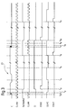
Deux fois par vingt-quatre heures, la rotation de la came 8 provoque la fermeture des lames du contacteur 2. Conformément à ce qui a été expliqué plus haut, cette transition n'est pas nette mais comporte une série de rebonds espacés entre l'instant t0 et l'instant t1, conformément à ce qui est représenté dans le graphe du signal C à la figure 3. Cette série de rebonds peut durer d'une à deux minutes. Le signal C est échantillonné lors des flans descendants de chacune des impulsions d'horloge CLKM, qui, à l'instant t0 et t1 ont la même forme que les impulsions d'horloge CLKA.Twice every twenty-four hours, the rotation of the
Lorsque le signal C est échantillonné à l'instant t2, le contacteur 2 a changé d'état et par suite un signal de niveau logique haut est fourni à l'entrée D17. Au flan descendant suivant du signal d'horloge CLKM (instant t3), la sortie Q17, et donc le signal Ci, passent à leur niveau haut et un signal de niveau haut est donc fourni à l'entrée 19b de la porte XOR 19. Puisque la sortie Q18 ne passera pas à son niveau haut avant le flan descendant suivant du signal d'horloge CLKA, la sortie 19c de la porte XOR (référencée par l'indication EDGE sur la figure 2) passe également à son niveau haut à l'instant t3 et pour la durée d'une période d'horloge. Dans ces conditions, un signal de niveau logique haut est fourni à l'entrée de reset R20 de façon à ce que le signal CLENABLE passe à son niveau logique bas. La transmission du signal d'horloge CLKA vers l'entrée de base de temps CL17 est ainsi bloquée à partir de l'instant t3, de manière que le signal CLKM reste à son niveau logique bas et que le signal C ne soit plus échantillonné. Le signal Ci reste donc dans un état constant.When the signal C is sampled at the instant t 2 , the contactor 2 has changed state and consequently a signal of high logic level is supplied to the input D17. On the following falling edge of the clock signal CLKM (instant t 3 ), the output Q17, and therefore the signal C i , pass to their high level and a high level signal is therefore supplied to the
Le signal d'horloge CLKA peut avoir une période d'environ 1 minute, de manière que, par exemple, un choc qui provoquerait la fermeture des lames 2a et 2b avant l'instant t0 n'ait que peu de chance de se produire à l'instant où le signal C est échantillonné. Afin d'éliminer complètement ce risque, on peut envisager un autre mode de réalisation du circuit d'échantillonnage 3 dans lequel il faudrait qu'au moins deux échantillons consécutifs ou plus du signal C se trouvent dans le même état, pour s'assurer que le contacteur 2 a bien changé d'état, avant que l'état du signal Ci ne soit changé lui aussi. Les circuits anti-rebonds de l'art antérieur qui ont été décrits dans les pages d'introduction peuvent être utilisés dans d'autres modes de réalisation du circuit d'échantillonnage 3 pour détecter les ouvertures et/ou fermetures volontaires du contacteur 2.The clock signal CLKA can have a period of approximately 1 minute, so that, for example, a shock which would cause the closing of the
Le temps pendant lequel le signal C demeure nonéchantillonné est déterminé par le compteur 21 et peut correspondre au temps de fermeture théorique du contacteur 2. Dans le cas où le contacteur 2 est utilisé dans une montre électronique analogique dans laquelle il est fermé par une came actionnée par le canon des heures de la montre, ce temps devrait être situé entre 26 et 30 minutes. Lorsque le contacteur 2 est ouvert et que le signal d'horloge CLKM a la même forme que le signal d'horloge CLKA, le compteur 21 est remis à zéro lors de chaque flan descendant du signal CLKM. Toutefois, l'état logique bas du signal CLKM à partir de l'instant t3 permet au compteur 21 de compter un nombre prédéterminé de changement d'état du signal CLKM, tels que représentés aux instants t4 et t5, et de fournir une impulsion logique de niveau haut à sa sortie Q21 (référencée COUT sur la figure 2) lorsque ce nombre prédéterminé est atteint à l'instant t6. On remarquera que le signal Ci demeure constant au moins entre les instants t3 et t6, et qu'il n'est pas affecté par les changements dans l'état du contacteur 2 causé par des chocs ou des impacts ou de mauvais contacts, conformément à ce qui est indiqué par la référence 23 (figure 3), qui peuvent se produire pendant ce temps.The time during which the signal C remains unsampled is determined by the
L'impulsion fournie par la sortie Q21 est envoyée par l'intermédiaire de la porte OU 22 à l'entrée "set" S20 de la bascule RS 20, de façon à ce que le signal CLENABLE fourni par la sortie Q20 repasse dans un état logique haut. Le signal d'horloge CLKA peut maintenant être envoyé par l'intermédiaire de la porte ET 6 et du multiplexeur 12 à l'entrée de base de temps CL17, de manière qu'à partir de l'instant t6 le signal CLKM ait à nouveau la même forme que le signal de base de temps CLKA et que le signal C soit donc à nouveau échantillonné lors de chaque flan descendant du signal CLKM.The pulse provided by the Q21 output is sent via the
A l'instant t7, la came 8 a tourné d'un angle suffisant pour que les lames de contact 2a et 2b commencent à se séparer. Les rebonds entre les lames 2a et 2b continuent à se produire jusqu'à l'instant t8, après quoi les lames demeurent séparées en permanence. Le temps qui s'écoule entre les instants t7 et t8 peut être de l'ordre d'une à deux minutes. En conséquence, le signal C repasse dans son niveau logique bas. Lors du premier flan descendant du signal CLKM, c'est-à-dire à l'instant t9, ce signal bas est lu par la bascule 17. Lors du flan descendant suivant du signal CLKM, à l'instant t10, le niveau bas du signal C est transféré à la sortie Q17, de manière que le signal Ci passe également à son niveau bas.At time t 7 , the
Conformément à ce qui a été décrit plus haut, un changement dans l'état de la sortie Q17 se traduit par une différence entre les états des deux entrées 19a et 19b de la porte XOR 19 qui dure pendant un cycle du signal CLKA. En conséquence, une impulsion de niveau logique haut est fournie à l'entrée de reset R20 de la bascule RS 20. Ceci provoque le passage du signal CLENABLE à son niveau bas, et bloque à nouveau la réception du signal CLKA par la bascule 17, et également l'échantillonnage du signal C durant une période déterminée par le compteur 21. Lorsque le compteur 21 a compté un nombre prédéterminé de changements d'état du signal CLKC, à l'instant t11, la sortie Q21 produit une impulsion qui est envoyée à l'entrée set S20 pour faire repasser le signal CLENABLE à son niveau logique haut et permettre la reprise de l'échantillonnage du signal C.In accordance with what has been described above, a change in the state of the output Q17 results in a difference between the states of the two
Le changement dans l'état du signal Ci (figure 3) à l'instant t10 résulte d'une ouverture intentionnelle du contacteur 2. Toutefois, un tel changement peut aussi être provoqué par un mauvais contact après l'instant t6. La détection de ce mauvais contact provoquera l'interruption de l'échantillonnage du signal C durant le temps prédéterminé, déterminé par le compteur 21, et ainsi le signal Ci sera à son niveau bas durant cette période. Toutefois, le signal Ci a déjà fourni un signal bien défini représentatif de la fermeture du contacteur 2 entre l'instant t3 et l'instant t6 et cette commutation parasite n'aura donc pas d'effet sur le circuit 11. De plus, la période allant de l'instant t6 qui représente la fin du temps de fermeture théorique du contacteur 2, et l'instant t7 qui représente la fin du temps de fermeture réel du contacteur 2, est suffisamment courte par rapport au temps durant lequel le signal C cesse d'être échantillonné, pour empêcher le signal Ci de passer à son niveau logique haut avant l'instant t8.The change in the state of the signal C i (FIG. 3) at time t 10 results from an intentional opening of the contactor 2. However, such a change can also be caused by a bad contact after time t 6 . The detection of this bad contact will cause the sampling of signal C to be interrupted during the predetermined time, determined by the
De façon semblable, la fermeture prématurée du contacteur 2, avant l'instant t6 n'a pas d'effet sur le circuit 11 puisque l'état du signal Ci demeure dans son niveau haut pendant au moins le temps de fermeture théorique du contacteur, 2 tel que déterminé par le compteur 21.Similarly, the premature closing of the contactor 2, before the instant t 6 has no effect on the
L'échantillonnage du signal C ne s'interrompt pas lorsqu'une montre utilisant le circuit 11 est mise à l'heure. Toutefois, on notera que dans d'autres applications, une interruption d'échantillonnage peut être désirable. Par exemple, le signal d'horloge CLKB peut être relié à une entrée d'une autre porte ET, dont la sortie est reliée à l'entrée I1 du multiplexeur 12. Un autre circuit d'évaluation du temps étant fourni pour recevoir les impulsions produites par la sortie 19c du détecteur 4, et pour fournir un signal de niveau logique bas à l'autre entrée de la porte ET supplémentaire de façon à empêcher l'échantillonnage du signal C pour une autre durée prédéterminée. Si le signal d'horloge CLKB a une période de 20 ms, cette période peut être de l'ordre de 100 ms.The sampling of signal C does not stop when a
Finalement, on comprendra que d'autres modifications et/ou additions peuvent être apportées au circuit sans sortir de l'objet de la présente invention tel que défini par les revendications annexées.Finally, it will be understood that other modifications and / or additions can be made to the circuit without departing from the object of the present invention as defined by the appended claims.
Claims (7)
- Circuit for suppressing the effect of rebounds and parasitic commutations of a contactor (2) on a control signal (C) produced by said contactor (2), said control signal (C) being in either a first state corresponding to an open position of said contactor (2) or a second state corresponding to a closed position of said contactor (2), said contactor (2) intended to change from one of said positions to the other of said positions and to remain in said other position for a predetermined time, characterized in that said circuit comprises :- sampling means (3) for sampling said control signal (C) at a first sampling rate (CLKA) and for providing a output signal (Ci) being in either said first state or said second state,- detecting means (4) for determining the change of said output signal (Ci) from one of said states to the other of said states, and- sampling prevention means (5) for preventing said sampling means (3) from sampling said control signal (C) for said predetermined time in response to the change in state of said output signal (Ci), in order that said output signal (Ci) remains in said other state for at least said predetermined time.
- Circuit according to claim 1, characterized in that said detecting means (4) determines the change of state of said output signal (Ci) by detecting when two or more consecutive samples of said control signal (C) are in said other state.
- Circuit according to either of claims 1 or 2, characterized in that said contactor (2) is controlled by a rotary cam (8).
- Circuit according to claim 3, characterized in that it is used in an analog electronic watch having a shaft, said cam (8) being rotatably driven by said shaft when the watch is in normal operation.
- Circuit according to claim 4, characterized in that said shaft is an hours-hand shaft.
- Circuit according to either of claims 4 or 5, characterized in that said watch comprises a rotatable time-setting crown (14) and in that said cam (8) is rotatably driven by said crown (14) while said watch is time-set.
- Circuit according to claim 6, characterized in that said sampling prevention means (5) is adapted to be inoperable when said watch is in a time-setting position, and in that, during this time-setting, said sampling means (3) is adapted to sample said control signal at a second selected sampling rate (CLKB).
Applications Claiming Priority (2)
| Application Number | Priority Date | Filing Date | Title |
|---|---|---|---|
| CH820/93 | 1993-03-18 | ||
| CH820/93A CH684622B5 (en) | 1993-03-18 | 1993-03-18 | Circuit to remove the effects of rebounds a switch and watch comprising such a circuit. |
Publications (2)
| Publication Number | Publication Date |
|---|---|
| EP0616272A1 EP0616272A1 (en) | 1994-09-21 |
| EP0616272B1 true EP0616272B1 (en) | 1997-07-30 |
Family
ID=4195956
Family Applications (1)
| Application Number | Title | Priority Date | Filing Date |
|---|---|---|---|
| EP94103849A Expired - Lifetime EP0616272B1 (en) | 1993-03-18 | 1994-03-12 | Circuit for suppressing the bouncing effects during closing and opening of a contact in a watch |
Country Status (7)
| Country | Link |
|---|---|
| US (1) | US5500836A (en) |
| EP (1) | EP0616272B1 (en) |
| JP (1) | JP3507123B2 (en) |
| CH (1) | CH684622B5 (en) |
| DE (1) | DE69404515T2 (en) |
| HK (1) | HK1001742A1 (en) |
| TW (1) | TW271468B (en) |
Families Citing this family (3)
| Publication number | Priority date | Publication date | Assignee | Title |
|---|---|---|---|---|
| US7391241B2 (en) * | 2004-11-15 | 2008-06-24 | Texas Instruments Incorporated | Bidirectional deglitch circuit |
| US7847614B2 (en) * | 2007-05-30 | 2010-12-07 | Kyocera Corporation | Switch noise reduction device and method using counter |
| JP7013044B2 (en) | 2020-06-25 | 2022-01-31 | 有限会社タクショー | Cleaner device for steel plate |
Family Cites Families (6)
| Publication number | Priority date | Publication date | Assignee | Title |
|---|---|---|---|---|
| US4138613A (en) * | 1974-08-14 | 1979-02-06 | Kabushiki Kaisha Daini Seikosha | Switching circuit |
| GB1500406A (en) * | 1974-08-14 | 1978-02-08 | Seiko Instr & Electronics | Switching circuits |
| JPS51115869A (en) * | 1975-04-03 | 1976-10-12 | Seiko Instr & Electronics Ltd | Time correction device of electronic clock |
| JPS54135573A (en) * | 1978-03-13 | 1979-10-20 | Seiko Epson Corp | Time correction system |
| JPS5575351A (en) * | 1978-12-01 | 1980-06-06 | Hitachi Denshi Ltd | Input line switching circuit |
| EP0274035B1 (en) * | 1986-12-03 | 1991-01-23 | Eta SA Fabriques d'Ebauches | Circuit for shaping the signal produced by a contact |
-
1993
- 1993-03-18 CH CH820/93A patent/CH684622B5/en not_active IP Right Cessation
-
1994
- 1994-02-08 TW TW083101077A patent/TW271468B/zh active
- 1994-03-12 DE DE69404515T patent/DE69404515T2/en not_active Expired - Lifetime
- 1994-03-12 EP EP94103849A patent/EP0616272B1/en not_active Expired - Lifetime
- 1994-03-14 US US08/213,143 patent/US5500836A/en not_active Expired - Lifetime
- 1994-03-18 JP JP07293794A patent/JP3507123B2/en not_active Expired - Fee Related
-
1998
- 1998-01-26 HK HK98100680A patent/HK1001742A1/en not_active IP Right Cessation
Also Published As
| Publication number | Publication date |
|---|---|
| JPH06300867A (en) | 1994-10-28 |
| HK1001742A1 (en) | 1998-07-03 |
| TW271468B (en) | 1996-03-01 |
| US5500836A (en) | 1996-03-19 |
| EP0616272A1 (en) | 1994-09-21 |
| DE69404515D1 (en) | 1997-09-04 |
| CH684622GA3 (en) | 1994-11-15 |
| DE69404515T2 (en) | 1998-02-26 |
| JP3507123B2 (en) | 2004-03-15 |
| CH684622B5 (en) | 1995-05-15 |
Similar Documents
| Publication | Publication Date | Title |
|---|---|---|
| EP0143279A1 (en) | Watch with analogous and numerical display | |
| EP1081563A1 (en) | Bracelet type watch | |
| EP1798611A1 (en) | Timepiece including a striking mechanism with instant triggering | |
| EP1798610A1 (en) | Timepiece including a single-pawl striking mechanism | |
| EP0616272B1 (en) | Circuit for suppressing the bouncing effects during closing and opening of a contact in a watch | |
| EP0064023B1 (en) | Time correcting means for an electronic clock | |
| EP0060806B1 (en) | Method of reducing the power consumption of a stepping motor, and device for carrying out this method | |
| EP0274035B1 (en) | Circuit for shaping the signal produced by a contact | |
| EP0064025B1 (en) | Electronic watch having fixed control means | |
| EP3264199A1 (en) | Timepiece comprising a switching device of a clockwork mechanism | |
| EP1207439A1 (en) | Electronic watch with capacitive switches on its cover glass | |
| CA2059133C (en) | Control device for the timed release of a mechanism | |
| EP0135104B1 (en) | Method and device for the control of a stepping motor | |
| CH688950B5 (en) | Synchronization device of an analog display with an electronic counter in a timepiece. | |
| EP0221363A1 (en) | Analogous electronic watch | |
| CH691090A5 (en) | Watch including means for detecting the failure of the power source. | |
| EP1521364B1 (en) | Method and apparatus for filtering signals generated by a piezoelectric accelerometer, and application in a portable object such as a watch | |
| EP0027250A1 (en) | Clockwork with display of seconds on demand | |
| EP0203330A1 (en) | Electronic time piece with a detector of the end of the life span of the battery | |
| EP0875807B1 (en) | Electronic timepiece powered by a generator driven by a mechanical energy source | |
| EP0171782B1 (en) | Electronic time piece with a possibility of adjusting the seconds indication | |
| CH714728A2 (en) | Bell mechanism for watch movement. | |
| EP0883261B1 (en) | Circuit for detecting reception error in an asynchronous transmission | |
| EP3779611B1 (en) | Electromechanical watch | |
| EP0006384A1 (en) | Synchronisation device using a received digital signal and transmission system including such a device |
Legal Events
| Date | Code | Title | Description |
|---|---|---|---|
| PUAI | Public reference made under article 153(3) epc to a published international application that has entered the european phase |
Free format text: ORIGINAL CODE: 0009012 |
|
| AK | Designated contracting states |
Kind code of ref document: A1 Designated state(s): DE FR GB NL |
|
| 17P | Request for examination filed |
Effective date: 19941004 |
|
| 17Q | First examination report despatched |
Effective date: 19960306 |
|
| GRAG | Despatch of communication of intention to grant |
Free format text: ORIGINAL CODE: EPIDOS AGRA |
|
| GRAH | Despatch of communication of intention to grant a patent |
Free format text: ORIGINAL CODE: EPIDOS IGRA |
|
| GRAH | Despatch of communication of intention to grant a patent |
Free format text: ORIGINAL CODE: EPIDOS IGRA |
|
| GRAA | (expected) grant |
Free format text: ORIGINAL CODE: 0009210 |
|
| AK | Designated contracting states |
Kind code of ref document: B1 Designated state(s): DE FR GB NL |
|
| REF | Corresponds to: |
Ref document number: 69404515 Country of ref document: DE Date of ref document: 19970904 |
|
| GBT | Gb: translation of ep patent filed (gb section 77(6)(a)/1977) |
Effective date: 19970925 |
|
| PLBE | No opposition filed within time limit |
Free format text: ORIGINAL CODE: 0009261 |
|
| STAA | Information on the status of an ep patent application or granted ep patent |
Free format text: STATUS: NO OPPOSITION FILED WITHIN TIME LIMIT |
|
| 26N | No opposition filed | ||
| REG | Reference to a national code |
Ref country code: GB Ref legal event code: IF02 |
|
| PGFP | Annual fee paid to national office [announced via postgrant information from national office to epo] |
Ref country code: GB Payment date: 20050225 Year of fee payment: 12 |
|
| PG25 | Lapsed in a contracting state [announced via postgrant information from national office to epo] |
Ref country code: GB Free format text: LAPSE BECAUSE OF NON-PAYMENT OF DUE FEES Effective date: 20060312 |
|
| GBPC | Gb: european patent ceased through non-payment of renewal fee |
Effective date: 20060312 |
|
| PGFP | Annual fee paid to national office [announced via postgrant information from national office to epo] |
Ref country code: NL Payment date: 20110225 Year of fee payment: 18 |
|
| PGFP | Annual fee paid to national office [announced via postgrant information from national office to epo] |
Ref country code: FR Payment date: 20110412 Year of fee payment: 18 Ref country code: DE Payment date: 20110308 Year of fee payment: 18 |
|
| REG | Reference to a national code |
Ref country code: NL Ref legal event code: V1 Effective date: 20121001 |
|
| REG | Reference to a national code |
Ref country code: FR Ref legal event code: ST Effective date: 20121130 |
|
| PG25 | Lapsed in a contracting state [announced via postgrant information from national office to epo] |
Ref country code: FR Free format text: LAPSE BECAUSE OF NON-PAYMENT OF DUE FEES Effective date: 20120402 |
|
| REG | Reference to a national code |
Ref country code: DE Ref legal event code: R119 Ref document number: 69404515 Country of ref document: DE Effective date: 20121002 |
|
| PG25 | Lapsed in a contracting state [announced via postgrant information from national office to epo] |
Ref country code: NL Free format text: LAPSE BECAUSE OF NON-PAYMENT OF DUE FEES Effective date: 20121001 |
|
| PG25 | Lapsed in a contracting state [announced via postgrant information from national office to epo] |
Ref country code: DE Free format text: LAPSE BECAUSE OF NON-PAYMENT OF DUE FEES Effective date: 20121002 |