EP0614280A1 - Semiconductor integrated circuit - Google Patents
Semiconductor integrated circuit Download PDFInfo
- Publication number
- EP0614280A1 EP0614280A1 EP94103119A EP94103119A EP0614280A1 EP 0614280 A1 EP0614280 A1 EP 0614280A1 EP 94103119 A EP94103119 A EP 94103119A EP 94103119 A EP94103119 A EP 94103119A EP 0614280 A1 EP0614280 A1 EP 0614280A1
- Authority
- EP
- European Patent Office
- Prior art keywords
- bipolar transistor
- power supply
- base
- npn bipolar
- collector
- Prior art date
- Legal status (The legal status is an assumption and is not a legal conclusion. Google has not performed a legal analysis and makes no representation as to the accuracy of the status listed.)
- Granted
Links
- 239000004065 semiconductor Substances 0.000 title claims description 19
- 238000010276 construction Methods 0.000 abstract 1
- IGRGLGHQFJOWOD-UHFFFAOYSA-N 8-[[ethyl(pyridin-4-ylmethyl)amino]methyl]-7-hydroxy-4-(2-oxochromen-3-yl)chromen-2-one Chemical compound OC=1C=CC=2C(C=3C(OC4=CC=CC=C4C=3)=O)=CC(=O)OC=2C=1CN(CC)CC1=CC=NC=C1 IGRGLGHQFJOWOD-UHFFFAOYSA-N 0.000 description 8
- 238000010586 diagram Methods 0.000 description 5
- 238000000034 method Methods 0.000 description 4
- 230000007423 decrease Effects 0.000 description 2
- 238000013459 approach Methods 0.000 description 1
- 238000004519 manufacturing process Methods 0.000 description 1
- 230000008054 signal transmission Effects 0.000 description 1
Images


Classifications
-
- H—ELECTRICITY
- H03—ELECTRONIC CIRCUITRY
- H03K—PULSE TECHNIQUE
- H03K19/00—Logic circuits, i.e. having at least two inputs acting on one output; Inverting circuits
- H03K19/01—Modifications for accelerating switching
- H03K19/013—Modifications for accelerating switching in bipolar transistor circuits
- H03K19/0136—Modifications for accelerating switching in bipolar transistor circuits by means of a pull-up or down element
Abstract
Description
- The present invention relates to a logic circuit and semiconductor integrated circuit device, and more particularly to technology effective for use in a Non Threshold Logic (NTL) circuit, a Super Push-pull Logic (SPL) circuit and further high-speed logical integrated circuits using these logic circuits as a basic circuit, for example.
- The NTL circuit is proposed as a high-speed and low electric power consuming digital logical circuit. For example, a SPL circuit and the like in which an Active Pull-Down (APD) circuit is provided in said NTL circuit are disclosed in Japanese Unexamined Provisional Publication, No. 3-64123 (prior art 1). Further, in order to enhance the collector response of the SPL circuit, a SPL-B circuit is also proposed in Japanese Unexamined Provisional Publication, No. 3-267817 (prior art 2).
- Fig. 1 is a circuit diagram showing one example of the conventional SPL circuit (prior art 1). As shown in Fig. 1, the conventional SPL circuit has a phase splitting circuit comprising a bipolar transistor Q21 and resistive elements R21 and R23 which are connected in series between a positive power supply terminal 1 and a negative
power supply terminal 2. An input signal VIN is input into a base of the transistor Q21. In between the positive power supply terminal 1 and the negativepower supply terminal 2, a bipolar transistor Q23 and a resistive element R24 are connected in series, and a negativepower supply terminal 3 is connected to a base of the transistor Q23. A capacity C22 is connected between a node A2 connecting the transistor Q21 and the resistive element R23 and a node A3 connecting the transistor Q23 and the resistive element R24. Further, a bipolar transistor Q22 and a bipolar transistor Q24 are connected in series between the positive power supply terminal 1 and the negativepower supply terminal 2, a base of the transistor Q22 is connected to a node A1 and a base of the transistor Q24 is connected to the node A3. Both an emitter of the transistor Q22 and a collector of the transistor Q24 are connected to an output terminal VOUT. - There exists a stray capacitance CC3 between the collector node (Node A1) of this phase splitting circuit and the negative
power supply terminal 2. In this case, when the level of an input signal VIN is high, the transistor Q21 is turned on so that the stray capacitance CC3 in the collector node (Node A1) is quickly discharged through the transistor Q21. - When the level of the input signal VIN is low, however, the stray capacity CC3 of the collector node (Node A1) is passively charged through the resistive element R21 because the transistor Q21 is at the off-state. Therefore, the raising of the potential at the collector node (Node A1) becomes slow according to the time constant determined by the product of a value of the resistive element R21 and the stray capacity CC3, and there was a problem therefore that the propagation delay time responding to the low level change of the input signal VIN becomes longer.
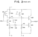
- As one of approaches to improve such problem, the SPL-B circuit is proposed. Fig. 2 is a circuit diagram showing the constitution of the SPL-B circuit (prior art 2). In Fig. 2, the same numeral is used for the elements or parts which have the same function as those shown in Fig. 1 and detail explanation will be omitted. As shown in Fig. 2, the conventional SPL-B circuit is a circuit in which a P-channel MOSFET Q5 is connected in parallel with a resistive element R21 in a phase splitting circuit area comprising a transistor Q21 and resistive elements R21 and R23 in the SPL circuit. To a gate of this MOSFET Q5, the input terminal VIN is connected.
- In this SPL-B circuit, the stray capacity CC2 of the collector node (node A1) is actively and quickly charged through the P-channel MOS transistor Q5 because the transistor Q5 is turned on when the level of the input signal VIN is low. On the other hand, when the level of the input signal VIN is high, the P-channel MOSFET Q5 is in off-state and therefore does not prevent a quick discharge of the collector node (node A1) through the transistor Q21 in the phase splitting circuit area.
- This improved SPL-B circuit was aimed to charge the collector node at high-speed. The MOS transistor, however, generally has a low ability of the current drive. Furthermore, there was another problem in the SPL-B circuit that the assembly process obviously becomes comprehensive because the assembly process for the MOS transistor is needed in addition to the assembly process for a bipolar transistor since the MOS transistor must be combined into the SPL circuit comprising the bipolar transistor.
- There was other problem in this circuit that the input capacity against the input signal is increased by the input capacity of the P-channel MOSFET Q5 so that the propagation delay time becomes longer because switching of the P-channel MOSEFT Q5 is made by the input signal VIN.
- It is therefore an object of the present invention to provide a semiconductor integrated circuit capable of making a collector response of a SPL circuit at high-speed without using the MOS transistor having a lower driving capacity and requiring more complicated fabrication process.
- According to the present invention, there is provided a semiconductor integrated circuit comprising: a signal input terminal; an NPN bipolar transistor, a base of which being connected to said signal input terminal; a power supply terminal; a resistive element, one end of which being is connected to a collector of said NPN bipolar transistor and another end thereof being connected to said power supply terminal; and a PNP bipolar transistor, a collector of which being is connected to a collector of said NPN transistor and an emitter of said PNP bipolar transistor being connected to said power supply terminal.
- According to the present invention, a signal to turn on said PNP bipolar transistor can be led through a capacitative load element etc., it taken from an emitter node not directly related with the logical signal transmission, therefore the input capacity at the input side of the circuit is not increased and the propagation delay time does not become longer.
- In addition, the semiconductor integrated circuit according to the present invention can be assembled by lesser steps than the conventional circuit (the SPL-B circuit) using the P-channel MOSFET because all constitution elements can be constructed with bipolar transistors in the present invention.
- Further, regarding the relationship between the wiring capacity and the gate delay time, the semiconductor integrated circuit according to the present invention can be increased in the speed by 84% compared to the conventional semiconductor integrated circuit, for example when the wiring has the capacity value of 0.4 pF.
- Fig. 1 is a circuit diagram showing a semiconductor integrated circuit of a prior art 1,
- Fig. 2 is a circuit diagram showing another semiconductor integrated circuit of a
prior art 2, - Fig. 3 is a circuit diagram showing a semiconductor integrated circuit according to an embodiment of the present invention, and
- Fig. 4 is a graph showing the relationship between the wiring capacity and the gate delay time.
- The present invention will now be described more fully hereinafter with reference to Fig. 3, in which a preferred embodiment of the present invention is shown. This embodiment relates to a semiconductor integrated circuit comprising a NTL circuit including a PNP transistor. In this semiconductor integrated circuit, a base of a first NPN bipolar transistor Q1 is connected to a signal input terminal VIN. A collector of the first NPN transistor Q1 is connected to one end of a first resistive element R1. To the node A1 between the transistor Q1 and the resistive element R1, a collector of a first PNP transistor Q11 and a base of a second NPN transistor Q2 are connected.
- Another end of the first resistive element R1, an emitter of the first PNP transistor Q11, one end of a second resistive element R2 and a collector Of the second NPN transistor Q2 are connected to a positive power supply terminal 1. To another end of the second resistive element R2, a base of the first PNP transistor Q11 and a collector of a third NPN transistor Q3 are connected. To an emitter of the first NPN transistor Q1, one end of a third resistive element R3 is connected through a node A2. Another end of the third resistive element R3 is connected to a first negative
power supply terminal 2, and one end of a fourth resistive element R4 and a base of a fourth NPN transistor Q4 are connected to an emitter of the third NPN transistor through a node A3. - An emitter of the second NPN transistor Q2 and a collector of said fourth NPN transistor Q4 are connected to a signal output terminal VOUT. Another end of the fourth resistive element R4 and an emitter of the fourth NPN transistor Q4 are connected to the first negative
power supply terminal 2. A secondnegative power terminal 3 is connected to a base of the third NPN transistor Q3. Further, a capacitative load element C1 is connected between a base of the first PNP transistor Q11 and the emitter of the first NPN transistor Q1, and a capacitative load element C2 is connected between the emitter of the first NPN transistor Q1 and the base of the fourth NPN transistor Q4. - Then, the operation of the semiconductor integrated circuit thus constructed according to the present embodiment will be explained. When a low level of signal is entered into the signal input terminal VIN, the NPN transistor Q1 is turned off. At this moment, the potential at the emitter node (Mode A2) of the transistor Q1 decreases and therefore the potential at the base node (Mode A4) of the PNP transistor Q11 also decreases temporally through the capacitative load element C1. Therefore, the transistor Q11 is turned on and the collector node (Mode A1) of the NPN transistor Q1 is actively and quickly charged by a large collector current flowing into the PNP bipolar transistor Q11 having a high ability of current drive.
- When said collector node (Mode A1) is charged up to the potential of positive power supply terminal 1, the potential between the emitter and the collector of the PNP bipolar transistor Q11 falls down to 0 bolt and then the PNP bipolar transistor Q11 is turned off.
- Fig. 4 is a graph prepared by plotting the wiring capacity on X-axis and the gate delay time on Y-axis to show the relationship between the wiring capacity and the gate delay time. Referring Fig. 4, it is clearly indicating that the semiconductor integrated circuit according to the present invention has shorter gate delay time than the conventional semiconductor integrated circuit (prior art 1). For example, when the wiring capacity has the value of 0.4 pF, the present invention can increase the speed by 84% compared to the conventional semiconductor integrated circuit.
Claims (3)
- A semiconductor integrated circuit comprising:
a signal input terminal (VIN),
an NPN bipolar transistor (Q1), a base of which being connected to said signal input terminal,
a power supply terminal (1), and
a resistive element (R1), one end of which being connected to a collector of said NPN bipolar transistor, and another end of which being connected to said power supply terminal,
characterized by further comprising,
a PNP bipolar transistor (Q11), a collector of which being connected to a collector of said NPN bipolar transistor, and an emitter of which being connected to said power supply terminal. - The semiconductor integrated circuit according to claim 1, characterized by further comprising:
a capacitative load element (C1) connected between a base of said PNP bipolar transistor (Q11) and an emitter of said NPN bipolar transistor (Q1), and
a bias circuit (R2,R4,Q3) for biasing a low voltage to a base of said NPN bipolar transistor. - A semiconductor integrated circuit comprising;
a signal input terminal (VIN),
a signal output terminal (VOUT),
a positive power supply terminal (1),
a first negative power supply terminal (2),
a second negative power supply terminal (3),
a first NPN bipolar transistor (Q1), a base of which being connected to said signal input terminal,
a first resistive element (R1) connected between a collector of said first NPN bipolar transistor and said positive power supply terminal,
a second NPN bipolar transistor (Q2), a base of which being connected to said collector of said first NPN bipolar transistor, a collector of which being connected to said positive power supply terminal, and an emitter of which being connected to said signal output terminal,
a third NPN bipolar transistor (Q3), a collector of which being connected to said base of said PNP bipolar transistor and, a base of which being connected to said second negative power supply terminal,
a fourth NPN bipolar transistor (Q4), a base of which being connected to an emitter of said third NPN bipolar transistor, a collector of which being connected to said signal output terminal, and an emitter of which being connected to said first negative power supply terminal,
a third resistive element (R3) connected between an emitter of said first NPN bipolar transistor and said first negative power supply terminal,
a fourth resistive element (R4), one end of which being connected to said base of said fourth NPN bipolar transistor and said emitter of said third NPN bipolar transistor, and another end of which being connected to said second negative power supply terminal, and
a second capacitative load element (C2) connected between said emitter of said first NPN bipolar transistor and said base of said fourth NPN bipolar transistor,
characterized by further comprising,
a PNP bipolar transistor (Q11), a collector of which being connected to said collector of said first NPN bipolar transistor, and an emitter of which being connected to said positive power supply terminal,
a first capacitive load element (C1) connected between said base of said PNP bipolar transistor and said emitter of said first NPN bipolar transistor, and
a second resistive element (R2) connected between a base of said PNP bipolar transistor and said positive power supply terminal.
Applications Claiming Priority (2)
| Application Number | Priority Date | Filing Date | Title |
|---|---|---|---|
| JP5040796A JP2783108B2 (en) | 1993-03-02 | 1993-03-02 | Semiconductor integrated circuit |
| JP40796/93 | 1993-03-02 |
Publications (2)
| Publication Number | Publication Date |
|---|---|
| EP0614280A1 true EP0614280A1 (en) | 1994-09-07 |
| EP0614280B1 EP0614280B1 (en) | 1997-08-06 |
Family
ID=12590591
Family Applications (1)
| Application Number | Title | Priority Date | Filing Date |
|---|---|---|---|
| EP94103119A Expired - Lifetime EP0614280B1 (en) | 1993-03-02 | 1994-03-02 | Semiconductor integrated circuit |
Country Status (4)
| Country | Link |
|---|---|
| US (1) | US5495099A (en) |
| EP (1) | EP0614280B1 (en) |
| JP (1) | JP2783108B2 (en) |
| DE (1) | DE69404702T2 (en) |
Cited By (1)
| Publication number | Priority date | Publication date | Assignee | Title |
|---|---|---|---|---|
| EP0903857A1 (en) * | 1997-09-19 | 1999-03-24 | Sony Corporation | Pulse output circuit |
Citations (7)
| Publication number | Priority date | Publication date | Assignee | Title |
|---|---|---|---|---|
| EP0050033A2 (en) * | 1980-10-13 | 1982-04-21 | Fujitsu Limited | A line driver circuit including a protective circuit against excess current |
| JPS6157121A (en) * | 1984-08-29 | 1986-03-24 | Fujitsu Ltd | Ttl circuit |
| EP0191165A1 (en) * | 1985-01-15 | 1986-08-20 | Texas Instruments Incorporated | Adjustable speed up circuit for TTL-type gates |
| EP0317890A2 (en) * | 1987-11-24 | 1989-05-31 | Fairchild Semiconductor Corporation | TTL circuit with increased transient drive |
| US5089724A (en) * | 1990-11-30 | 1992-02-18 | International Business Machines Corporation | High-speed low-power ECL/NTL circuits with AC-coupled complementary push-pull output stage |
| JPH04100315A (en) * | 1990-08-18 | 1992-04-02 | Hitachi Ltd | Logic circuit |
| US5206546A (en) * | 1990-03-16 | 1993-04-27 | Hitachi, Ltd. | Logic circuit including variable impedance means |
Family Cites Families (7)
| Publication number | Priority date | Publication date | Assignee | Title |
|---|---|---|---|---|
| JPS57162837A (en) * | 1981-04-01 | 1982-10-06 | Nec Corp | Inverter circuit |
| US4737665A (en) * | 1985-01-15 | 1988-04-12 | Texas Instruments Incorporated | Adjustable speed up circuit for TTL-type gates |
| US5283480A (en) * | 1988-04-02 | 1994-02-01 | Hitachi, Ltd. | Semiconductor integrated circuit device with a plurality of logic circuits having active pull-down functions |
| JPH0364123A (en) * | 1989-08-02 | 1991-03-19 | Hitachi Ltd | Semiconductor integrated circuit |
| JPH03267817A (en) * | 1990-03-16 | 1991-11-28 | Hitachi Ltd | Logic circuit and semiconductor integrated circuit device |
| US5237214A (en) * | 1990-08-18 | 1993-08-17 | Hitachi, Ltd. | High speed logic circuit and semiconductor integrated circuit device including variable impedance to provide reduced power consumption |
| US5334886A (en) * | 1992-11-13 | 1994-08-02 | International Business Machines Corporation | Direct-coupled PNP transistor pull-up ECL circuits and direct-coupled complementary push-pull ECL circuits |
-
1993
- 1993-03-02 JP JP5040796A patent/JP2783108B2/en not_active Expired - Fee Related
-
1994
- 1994-02-28 US US08/202,826 patent/US5495099A/en not_active Expired - Lifetime
- 1994-03-02 DE DE69404702T patent/DE69404702T2/en not_active Expired - Fee Related
- 1994-03-02 EP EP94103119A patent/EP0614280B1/en not_active Expired - Lifetime
Patent Citations (7)
| Publication number | Priority date | Publication date | Assignee | Title |
|---|---|---|---|---|
| EP0050033A2 (en) * | 1980-10-13 | 1982-04-21 | Fujitsu Limited | A line driver circuit including a protective circuit against excess current |
| JPS6157121A (en) * | 1984-08-29 | 1986-03-24 | Fujitsu Ltd | Ttl circuit |
| EP0191165A1 (en) * | 1985-01-15 | 1986-08-20 | Texas Instruments Incorporated | Adjustable speed up circuit for TTL-type gates |
| EP0317890A2 (en) * | 1987-11-24 | 1989-05-31 | Fairchild Semiconductor Corporation | TTL circuit with increased transient drive |
| US5206546A (en) * | 1990-03-16 | 1993-04-27 | Hitachi, Ltd. | Logic circuit including variable impedance means |
| JPH04100315A (en) * | 1990-08-18 | 1992-04-02 | Hitachi Ltd | Logic circuit |
| US5089724A (en) * | 1990-11-30 | 1992-02-18 | International Business Machines Corporation | High-speed low-power ECL/NTL circuits with AC-coupled complementary push-pull output stage |
Non-Patent Citations (2)
| Title |
|---|
| PATENT ABSTRACTS OF JAPAN vol. 10, no. 221 (E - 424) 2 August 1986 (1986-08-02) * |
| PATENT ABSTRACTS OF JAPAN vol. 16, no. 336 (E - 1237) 21 July 1992 (1992-07-21) * |
Cited By (2)
| Publication number | Priority date | Publication date | Assignee | Title |
|---|---|---|---|---|
| EP0903857A1 (en) * | 1997-09-19 | 1999-03-24 | Sony Corporation | Pulse output circuit |
| US5952736A (en) * | 1997-09-19 | 1999-09-14 | Sony Corporation | Pulse output circuit |
Also Published As
| Publication number | Publication date |
|---|---|
| DE69404702D1 (en) | 1997-09-11 |
| JPH06252739A (en) | 1994-09-09 |
| JP2783108B2 (en) | 1998-08-06 |
| US5495099A (en) | 1996-02-27 |
| DE69404702T2 (en) | 1998-01-29 |
| EP0614280B1 (en) | 1997-08-06 |
Similar Documents
| Publication | Publication Date | Title |
|---|---|---|
| EP0463890B1 (en) | Emitter coupled logic device | |
| EP0270029B1 (en) | Logic circuit | |
| US4880998A (en) | Bipolar transistor and CMOS transistor logic circuit having improved discharge capabilities | |
| EP0361841A2 (en) | Bicmos logic circuit | |
| US4806797A (en) | bi-CMOS buffer cascaded to CMOS driver having PMOS pull-up transistor with threshold voltage greater than VBE of bi-CMOS bipolar pull-up transistor | |
| US5138195A (en) | Bi-CMOS logic circuit having full voltage swing and rapid turn-off | |
| US5864245A (en) | Output circuit with overvoltage protection | |
| US5495099A (en) | High speed super push-pull logic (SPL) circuit using bipolar technology | |
| EP0285157A2 (en) | Tri-state output circuit | |
| JP2561003B2 (en) | Active pull-down ECL circuit | |
| US5066874A (en) | Signal output circuit having bipolar transistor in output stage and arranged in cmos semiconductor integrated circuit | |
| US5107143A (en) | Signal output circuit included in bus driving integrated circuit | |
| US5097150A (en) | Bi-cmos logic circuit | |
| JP2544826B2 (en) | Semiconductor integrated circuit | |
| JP2003304151A (en) | Output driver circuit | |
| EP0465167B1 (en) | Non-threshold logic circuit | |
| KR930007564B1 (en) | Ecl circuit with fet full down load | |
| JP2899164B2 (en) | Emitter follower circuit | |
| JP2737729B2 (en) | ECL circuit | |
| KR100228839B1 (en) | Electronic circuit with high metastability-immunity | |
| JP3464864B2 (en) | ECL logic circuit | |
| JP2934265B2 (en) | Complementary MOS output circuit | |
| JP2511044B2 (en) | Logic circuit | |
| JP2998311B2 (en) | Logic circuit | |
| KR100247313B1 (en) | Logic circuit |
Legal Events
| Date | Code | Title | Description |
|---|---|---|---|
| PUAI | Public reference made under article 153(3) epc to a published international application that has entered the european phase |
Free format text: ORIGINAL CODE: 0009012 |
|
| AK | Designated contracting states |
Kind code of ref document: A1 Designated state(s): DE FR GB |
|
| 17P | Request for examination filed |
Effective date: 19941108 |
|
| 17Q | First examination report despatched |
Effective date: 19960417 |
|
| GRAG | Despatch of communication of intention to grant |
Free format text: ORIGINAL CODE: EPIDOS AGRA |
|
| GRAH | Despatch of communication of intention to grant a patent |
Free format text: ORIGINAL CODE: EPIDOS IGRA |
|
| GRAH | Despatch of communication of intention to grant a patent |
Free format text: ORIGINAL CODE: EPIDOS IGRA |
|
| GRAA | (expected) grant |
Free format text: ORIGINAL CODE: 0009210 |
|
| AK | Designated contracting states |
Kind code of ref document: B1 Designated state(s): DE FR GB |
|
| REF | Corresponds to: |
Ref document number: 69404702 Country of ref document: DE Date of ref document: 19970911 |
|
| ET | Fr: translation filed | ||
| PLBE | No opposition filed within time limit |
Free format text: ORIGINAL CODE: 0009261 |
|
| STAA | Information on the status of an ep patent application or granted ep patent |
Free format text: STATUS: NO OPPOSITION FILED WITHIN TIME LIMIT |
|
| 26N | No opposition filed | ||
| REG | Reference to a national code |
Ref country code: GB Ref legal event code: IF02 |
|
| REG | Reference to a national code |
Ref country code: GB Ref legal event code: 732E |
|
| REG | Reference to a national code |
Ref country code: FR Ref legal event code: TP |
|
| PGFP | Annual fee paid to national office [announced via postgrant information from national office to epo] |
Ref country code: GB Payment date: 20090225 Year of fee payment: 16 |
|
| PGFP | Annual fee paid to national office [announced via postgrant information from national office to epo] |
Ref country code: DE Payment date: 20090226 Year of fee payment: 16 |
|
| PGFP | Annual fee paid to national office [announced via postgrant information from national office to epo] |
Ref country code: FR Payment date: 20090316 Year of fee payment: 16 |
|
| GBPC | Gb: european patent ceased through non-payment of renewal fee |
Effective date: 20100302 |
|
| REG | Reference to a national code |
Ref country code: FR Ref legal event code: ST Effective date: 20101130 |
|
| PG25 | Lapsed in a contracting state [announced via postgrant information from national office to epo] |
Ref country code: FR Free format text: LAPSE BECAUSE OF NON-PAYMENT OF DUE FEES Effective date: 20100331 |
|
| PG25 | Lapsed in a contracting state [announced via postgrant information from national office to epo] |
Ref country code: DE Free format text: LAPSE BECAUSE OF NON-PAYMENT OF DUE FEES Effective date: 20101001 |
|
| PG25 | Lapsed in a contracting state [announced via postgrant information from national office to epo] |
Ref country code: GB Free format text: LAPSE BECAUSE OF NON-PAYMENT OF DUE FEES Effective date: 20100302 |