EP0612855A2 - A new compound with room temperature electrical resistivity comparable to that of elemental copper - Google Patents
A new compound with room temperature electrical resistivity comparable to that of elemental copper Download PDFInfo
- Publication number
- EP0612855A2 EP0612855A2 EP94101171A EP94101171A EP0612855A2 EP 0612855 A2 EP0612855 A2 EP 0612855A2 EP 94101171 A EP94101171 A EP 94101171A EP 94101171 A EP94101171 A EP 94101171A EP 0612855 A2 EP0612855 A2 EP 0612855A2
- Authority
- EP
- European Patent Office
- Prior art keywords
- copper
- present
- layer
- substrate
- room temperature
- Prior art date
- Legal status (The legal status is an assumption and is not a legal conclusion. Google has not performed a legal analysis and makes no representation as to the accuracy of the status listed.)
- Withdrawn
Links
Images

Classifications
-
- C—CHEMISTRY; METALLURGY
- C22—METALLURGY; FERROUS OR NON-FERROUS ALLOYS; TREATMENT OF ALLOYS OR NON-FERROUS METALS
- C22C—ALLOYS
- C22C9/00—Alloys based on copper
-
- H—ELECTRICITY
- H01—ELECTRIC ELEMENTS
- H01L—SEMICONDUCTOR DEVICES NOT COVERED BY CLASS H10
- H01L23/00—Details of semiconductor or other solid state devices
- H01L23/52—Arrangements for conducting electric current within the device in operation from one component to another, i.e. interconnections, e.g. wires, lead frames
- H01L23/522—Arrangements for conducting electric current within the device in operation from one component to another, i.e. interconnections, e.g. wires, lead frames including external interconnections consisting of a multilayer structure of conductive and insulating layers inseparably formed on the semiconductor body
- H01L23/532—Arrangements for conducting electric current within the device in operation from one component to another, i.e. interconnections, e.g. wires, lead frames including external interconnections consisting of a multilayer structure of conductive and insulating layers inseparably formed on the semiconductor body characterised by the materials
- H01L23/53204—Conductive materials
- H01L23/53209—Conductive materials based on metals, e.g. alloys, metal silicides
- H01L23/53228—Conductive materials based on metals, e.g. alloys, metal silicides the principal metal being copper
- H01L23/53233—Copper alloys
-
- H—ELECTRICITY
- H01—ELECTRIC ELEMENTS
- H01L—SEMICONDUCTOR DEVICES NOT COVERED BY CLASS H10
- H01L2924/00—Indexing scheme for arrangements or methods for connecting or disconnecting semiconductor or solid-state bodies as covered by H01L24/00
- H01L2924/0001—Technical content checked by a classifier
- H01L2924/0002—Not covered by any one of groups H01L24/00, H01L24/00 and H01L2224/00
Definitions
- the present invention relates to novel metal alloy compounds that exhibit room temperature electrical resistivity comparable to that of elemental copper. More specifically, the present invention relates to highly oxidation resistant compounds having low resistivity at room temperature comprising a body of stoichiometric copper germanide (Cu3Ge) containing about 1 to 15 atomic percent gallium and/or gold. Furthermore, the present invention relates to a method of preparing the highly oxidation resistant compounds.
- Cu3Ge stoichiometric copper germanide
- Copper because of its low resistivity, has been used for interconnect and contact application in VLSI and related technologies. However, copper exhibits a high diffusivity in silicon and is generally believed to be detrimental to the performance of silicon due to Cu-induced recombination centers which can reduce the minority carrier lifetime.
- copper silicide reacts readily with oxygen upon exposure to air or oxygen resulting in degradation of its electrical transport properties.
- Another possible solution to this problem is to alloy the copper with other metals. However, this typically results in an increase in the resistivity of the alloyed material.
- research is ongoing in an attempt to provide a material for semiconductor devices that has low resistivity and is highly stable when exposed to air or oxygen for use in interconnect and contact applications.
- the reference relates to a non-injecting ohmic contact for semiconductor devices using a copper-gold-germanium ternary alloy.
- This ternary alloy is formed by coating the base material which is directly bonded to the semiconductive body with a first layer of copper and a second layer of gold. The relative amounts by weight of the material is said to be strictly maintained in ratios from 1:1 to about 1:3 of copper to gold in the respective layers of the coating.
- U.S. Patent No. 3,468,659 to Belasco et al. provides a semiconductor contact alloy for forming ohmic contacts to n-type material, and for forming an emitter of an npn group III-V compound transistor. More specifically, the invention relates to a metal alloy, comprising gold, germanium, and a donor impurity such as tin, sulfur, selenium or tellurium to provide an emitter contact to P-type GaAs, or an ohmic contact to N-type material.
- This alloy which contains 30% Au, 65% Ge, and 5% donor impurity by weight, is said to withstand operating temperatures as high as the upper limit of a GaAs transistor.
- U.S. Patent No. 3,765,956 to Li relates to solid-state devices, and more particularly to melt-grown solid-state devices having unique operating characteristics and/or structure. Moreover, the reference describes a solid-state device containing melts, eutectics and intermettalics to improve these device characteristics by using melts of copper and germanium, germanium and gold and gallium, and copper and gold.
- U.S. Patent No. 4,786,469 to Weber et al. describes a grain refinement method for copper based metals in which the metal to be grain refined is alloyed with germanium or gallium.
- the copper based metals which have been successfully grained refined by the method of the invention include alpha-beta brasses, alpha-brasses, bronzes, gunmetals and the like thereof.
- U.S. Patent No. 5,001,536 to Fukuzawa et al. relates to multilayered-structure semiconductor device which has enhanced hole mobility and which can generate a sufficient signal current. More specifically, the reference provides a semiconductor device using an alloy of gold and germanium and nickel as electrodes.
- the present invention relates to novel metal alloy compounds that exhibit low electrical resistivity at room temperature. More specifically, it has been discovered that the incorporation of at least 1 to 15 atomic percent of gallium and/or at least 1 to 15 atomic percent gold into stoichiometric copper germanide (Cu3Ge) metal alloy compound results in a room temperature resistivity comparable to that of elemental copper or aluminum, but with superior chemical and electronic stability upon exposure to air or oxygen at high temperatures. In other words, the chemical and electrical stability of the compounds of the present invention are vastly superior to those compounds previously disclosed in the prior art.
- the compounds of the present invention do not exhibit any of the problems normally associated with the diffusion of copper into elemental and compound semiconductors which oftentimes lead to the degradation of the semiconductor device characteristics. Due to their robust electronic and thermal properties, the novel metal alloy compounds of the present invention are extremely useful as contacts and interconnections in Si and SiGe semiconductor devices.
- the present invention relates to a method of preparing the novel metal alloy compounds mentioned previously hereinabove by depositing sequential layers of gallium and/or gold prior to the deposition of a copper layer on to a semiconductor substrate which contains a layer of germanium thereon and thereafter annealing at a temperature in the range from about 150°C to about 500°C for 15 min. to about 3 hours.
- a method for preparing highly oxidation resistant compounds comprising the steps of: providing a semiconductor substrate having a Ge layer deposited thereon; depositing a layer of material on said substrate wherein said material is selected from the group of materials consisting of Ga, Au or mixtures of Ga and Au; depositing a layer of Cu on said material layer; and heating said substrate and material layers to a temperature in the range from about 150°C to about 500°C for a period of time from about 15 min. to about 3 hours to produce the stoichiometric Cu3Ge containing said material.
- the present invention also relates to the low resistivity compounds produced by the process of the present invention.
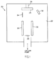
- Figure 1 is a schematic drawing which illustrates a typical apparatus used in the method of the invention.
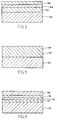
- Figure 2 is a schematic drawing showing the cross-section of a semiconductor substrate having a Ge layer deposited thereon and including the deposition of Ga and Cu layers using the sequential deposition method of the present invention prior to annealing.
- Figure 3 is a schematic drawing showing the annealed product formed containing the components described in Fig. 2.
- Figure 4 is a schematic drawing showing the cross-section of a semiconductor substrate having a Ge layer deposited thereon and including the deposition of Au and Cu layers using the sequential deposition method of the present invention prior to annealing.
- Figure 5 is a plot of the resistivity vs. temperature for (a) Cu3Ge substrate having 1-2 atomic % Ga incorporated therein and (b) Cu3Ge substrate having a mixture of Au and Ga incorporated therein.
- the compounds of the present invention are chemically stable, robust and do not exhibit any of the problems associated with the diffusion of copper into elemental and compound semiconductors which ultimately results in the degradation of the semiconductor device.
- the term robust is used herein to signify that the compounds of the present invention are highly resistant to oxidation when they are exposed to air or oxygen.
- the compounds of the present invention represent an advancement in the art due to their low electrical resistivity and oxidation resistance properties. The compounds of the present invention are therefore extremely useful for applications as interconnects and contacts in semiconductor devices.
- the incorporation of 1 to 15 atomic percent gallium and/or gold into a stoichiometric copper germanide (Cu3Ge) compound results in lowering the resistivity of the compound to a value that is comparable to that of elemental copper or aluminum. More preferably, the atomic percent of gallium and/or gold incorporated into the Cu3Ge compound is from 1 to 5. The most preferred range of gallium and/or gold incorporated into the stoichiometric Cu3Ge compound is from 1 to 3 atomic percent.
- the method of the present invention may be carried out in a typical E-beam evaporation apparatus as shown in Figure 1 or by other means well known in the art such as sputtering or boat evaporation.
- the preferred apparatus is an E-beam apparatus.
- the E-beam apparatus 20 includes a deposition chamber 22 having a semiconductor substrate 24 disposed on a turret 26 and a high vacuum pump not shown for evacuating the deposition chamber 22 prior to the initiation of the sequential deposition process.
- the E-beam apparatus 20 also includes a high current source 28 which causes effective emission of electrons from the source and magnetic poles 30 which are positioned adjacent to the current source 28 to cause bending of the electron beam.
- the apparatus 20 further includes a shutter 34 and a cryatal rate monitor 32 which are employed in the present apparatus to control the thickness of the films being deposited onto the surface of the semiconductor substrate.
- the film thickness which is being deposited is controlled by measuring the change of frequency on the surface of the cryatal rate monitor 32.
- the substrates employed by the present invention may be any semiconductor substrate well known in the art such as Si, SiGe, GaAs and the likes thereof.
- the semiconductor substrate is a single crystal which has a ⁇ 100 ⁇ crystal structure.
- the most preferred semiconductor substrate of the present invention is a Si ⁇ 100 ⁇ single crystal.
- the films employed by the present invention are prepared by methods well known in the art, such as chemical vapor deposition, evaporation and the like. Mixtures of the semiconductor substrates as defined above are also contemplated by the present invention.
- an epilayer of GaAs may be deposited on the surface of a Si ⁇ 100 ⁇ single crystal prior to the sequential deposition of the other elements.
- This GaAs epilayer which is formed on the surface of the Si substrate is prepared by molecular beam epitaxy or by any other suitable technique well known in the art for depositing such a layer.
- the substrate is placed into the E-beam apparatus 20 and then the deposition chamber 22 is pumped down to a low vacuum to remove any air or oxygen that may be present on the surface of the substrate or in the E-beam apparatus itself.
- the deposition chamber 22 is evacuated until a pressure reading of about 1x10 ⁇ 7 to about 1x10 ⁇ 8 Torr is obtained. Most preferably, this evacuation step is conducted until a constant pressure reading of about 1x10 ⁇ 7 Torr is obtained.
- germanium, gallium and/or gold, and copper are deposited onto the surface of the substrate at room temperature.
- these elements are essentially pure, however, minor amounts of impurities may be tolerated by the present invention. It is especially preferred that these compounds do not come into contact with air or oxygen during the deposition process since contact with air or oxygen will cause oxidation to occur.
- the sequential deposition process of the present invention is conducted in a vacuum or an inert gas atmosphere.
- germanium is first deposited onto the surface of the semiconductor substrate until a thin layer of about 70 to about 80 nm (about 700 to about 800 ⁇ ) is obtained. More preferably, the germanium is deposited so that a thin film of about 75 to about 77.5 nm (about 750 to about 775 ⁇ is obtained on the surface of the semiconductor substrate.
- Ge-substrate After forming the Ge-substrate, thin layers of gallium and/or gold are then deposited onto the surface of the thus formed Ge-substrate.
- gallium When gallium is used alone, a thin layer of about 5 to about 10 nm (about 50 to about 100 ⁇ ) is deposited on to the Ge-substrate. This layer thickness of gallium which is deposited corresponds to about 1 to about 3 atomic percent of gallium in the final product.
- the gold layer be embedded between two Ge layers.
- a thin layer of Ge of about 35 nm (about 350 ⁇ ) is first deposited onto the semiconductor substrate, followed by a thin layer of gold (5 nm (50 ⁇ )) and another layer of Ge (35 nm (350 ⁇ )).
- the total amount of Ge deposited should equate to 70 nm (700 ⁇ ).
- This thin layer of gold which is deposited corresponds to about 1-2 atomic percent of gold in the final product after annealing.
- the Ga layer has a film thickness of about 1 to about 5 nm (about 10 to about 50 ⁇ ) while the Au layer has a thickness of about 1 to about 5 nm (about 10 to about 50 ⁇ ).
- This film thickness of Ga and Au correspond to about 1-2 atomic % of Ga and 1-2 atomic % of Au in the final product.
- a thin layer of copper from about 50 to about 200 nm (about 500 to about 2000 ⁇ ) is then deposited onto the surface.
- the copper is deposited so that a thin layer of copper from about 120-140 nm (about 1200-1400 ⁇ ) is formed on the surface.
- the copper is deposited so that a thin layer of about 130 nm (about 1300 ⁇ ) is formed.
- the deposition of the various layers on to the semiconductor substrate surface is usually conducted at a temperature of about -200 to about +400°C.
- the deposition temperature of the various layers on to the semiconductor substrate surface is at room temperature.
- the substrate containing the deposited layers is then subjected to in-situ annealing either under vacuum or an inert gas atmosphere.
- the in-situ annealing process is conducted at a temperature from about 150 to about 500°C for a time period of about 15 minutes to 3 hours. More preferably, the in-situ annealing is conducted at a temperature of about 200 to about 450°C for a time period of about 15 min. to 1.5 hour. Most preferably, the annealing is conducted at atmosphere of about 400°C for 30 minutes.
- the present invention prevents copper oxidation from occurring by conducting the annealing process in a vacuum or an inert gas atmosphere. If an inert gas atmosphere is employed, the gases should be essentially pure containing little or no traces of oxygen or water. Suitable inert gases that may be employed by the present invention are He, Ar, N2 and the like.
- the electrical resistivity values of the compounds were determined using a four point probe method. Basically, the four point probe method measures the electrical resistivity of a substrate as a function of the temperature. By employing this method, the electrical resistivity of the compounds of the present invention are found to be in the range of about 2.6 to about 2.9 ⁇ cm at a temperature of 180°K from samples that have a total film thickness of about 200 nm (about 2000 ⁇ ). These values are comparable to those reported for elemental copper (2-2.5 ⁇ cm at room temperature). Additionally, the compounds prepared by the present invention are highly resistant to oxidation when exposed to air or oxygen therefore the compounds are applicable for use as contact and interconnections in semiconductor devices.
- the electrical resistivity values of the present invention are lower than the resistivity value reported for 200 nm (2000 ⁇ ) thick film of Cu3Ge which is reported to be 5-6 ⁇ cm. This is somewhat surprising since one skilled in the art would expect that the electrical resistivity should increase when additional components are added to the alloy.
- the semiconductor substrate employed in this example is a Si ⁇ 100 ⁇ single crystal.
- the Si substrate was loaded on to the turret of the E-beam apparatus as shown in Fig. 1. Thereafter, the system was evacuated to a partial pressure reading of about 1x10 ⁇ 7 Torr. After maintaining this pressure reading for a period of time, the sequential deposition of germanium, gallium and copper was initiated. This sequential process was carried under vacuum at room temperature thus avoiding contact with air or oxygen which may cause oxidation to occur.
- a thin film of germanium of about 70 nm (about 700 ⁇ ) was first deposited on to the surface of the Si ⁇ 100 ⁇ crystal. Thereafter, 5-10 atomic percent of gallium was deposited on to the surface of the Ge-film and a thin film of about 130 nm (about 1300 ⁇ ) of copper was deposited on top of the gallium film.
- Fig. 2 is a schematic drawing which illustrates the different layers which are deposited on to the Si substrate. More specifically, Fig. 2 is a schematic drawing showing one embodiment of the present invention wherein Ge, Ga and Cu are sequentially deposited onto the surface of a semiconductor substrate.
- the semiconductor substrate 50 is a ⁇ 100 ⁇ single crystal of Si.
- a thin layer of Ge 52 is deposited onto the surface of the semiconductor substrate 50.
- thin layers of Ga 54 and Cu 56 are deposited onto the Ge-containing substrate prior to the annealing process.
- Fig. 3 is a schematic drawing showing the final product formed after annealing.
- the Si semiconductor substrate 60 contains a layer of stoichiometric Cu3Ge 62 which has 1 to 2 atomic percent Ga 64 incorporated therein.
- Fig. 5(b) illustrates that by optimizing the Ga content reduction in the semiconductor upturn in ⁇ vs T results in low, and almost temperature independent electrical resistivity. This characteristic, coupled with the total resistance of this compound to oxidation, makes it extremely useful in applications for contacts and metallization.
- the compound of this comparative example was prepared in a similar manner as described in Example I except that no gallium was incorporated into the sequential deposition process.
- FIG. 4 is a schematic drawing illustrating the different layers which are sequentially deposited onto the Si substrate.
- the semiconductor substrate 70 is ⁇ 100 ⁇ Si.
- a thin layer of about 35 nm (about 350 ⁇ ) of Ge 72 is deposited onto the semiconductor substrate 70.
- a thin layer of Au 74 and another layer of Ge 76 of about 35 nm (about 350 ⁇ ) are deposited onto the substrate's surface so that the Au layer 74 is embedded between the Ge layers 72 and 76.
- a thin layer of Cu 78 is deposited onto the surface prior to annealing.
- the compound was prepared in accordance with the procedure described in Example I however a mixture of Ga and Au was incorporated instead of only Ga. After annealing, the final product is similar to Fig. 3 however the layer containing the stoichiometric Cu3Ge compound had 1-2 atomic % Ga and 1-2 atomic % Au incorporated therein.
- Fig. 5(a) illustrates the ⁇ vs T. graph for this example.
- the plot illustrates that by incorporating a mixture of Ga and Au into stoichiometric Cu3Ge results in a slight semiconductor upturn as compared to Example I. Despite this upturn in the ⁇ vs T. plot, the incorporation of Ga and Au resulted in a compound that has a room temperature resistivity of about 3.2 ⁇ cm, which is comparable that of elemental copper.
Landscapes
- Chemical & Material Sciences (AREA)
- Engineering & Computer Science (AREA)
- Materials Engineering (AREA)
- Mechanical Engineering (AREA)
- Metallurgy (AREA)
- Organic Chemistry (AREA)
- Physics & Mathematics (AREA)
- Condensed Matter Physics & Semiconductors (AREA)
- General Physics & Mathematics (AREA)
- Computer Hardware Design (AREA)
- Microelectronics & Electronic Packaging (AREA)
- Power Engineering (AREA)
- Electrodes Of Semiconductors (AREA)
- Physical Vapour Deposition (AREA)
- Physical Deposition Of Substances That Are Components Of Semiconductor Devices (AREA)
Abstract
The present invention relates to novel compounds that exhibit unusually low electrical resistivity at room temperature. More specifically, it has been discovered that the incorporation of at least 1 to 15 atomic percent of gallium and/or at least 1 to 15 atomic percent gold into stoichiometric copper germanide (Cu₃Ge) compound results in a room temperature resistivity comparable to elemental copper, but with superior chemical and electronic stability upon exposure to air or oxygen at high temperatures. Furthermore, the compounds of the present invention have none of the problems associated with the diffusion of copper into elemental and compound semiconductors which oftentimes lead to the degradation of the semiconductor device characteristics. Additionally, the present invention relates to a method of preparing the novel compounds mentioned previously hereinabove.
Description
- This application is related to pending U.S. application Serial No. 818,027 filed on January 7, 1992 to the same assignee. This application is also related to U.S. application Serial No. 876,669 filed on April 30, 1992 to the same assignee.
- The present invention relates to novel metal alloy compounds that exhibit room temperature electrical resistivity comparable to that of elemental copper. More specifically, the present invention relates to highly oxidation resistant compounds having low resistivity at room temperature comprising a body of stoichiometric copper germanide (Cu₃Ge) containing about 1 to 15 atomic percent gallium and/or gold. Furthermore, the present invention relates to a method of preparing the highly oxidation resistant compounds.
- The continued miniaturization of integrated circuits has brought about an increasing need to reduce the resistance in interconnect and contact metallurgy. In recent years, much effort has been focused on the use of metal silicides to fulfill this need. However, as semiconductor device dimensions become even smaller, both horizontally and vertically, silicides lose their attractiveness. The intrinsic resistivity of the silicides is high compared to metals, while the formation of self-aligned silicides consumes silicon in proportion to the thickness of the silicide that is formed. This consumption usually leads to junction leakage which is intolerable.
- Copper, because of its low resistivity, has been used for interconnect and contact application in VLSI and related technologies. However, copper exhibits a high diffusivity in silicon and is generally believed to be detrimental to the performance of silicon due to Cu-induced recombination centers which can reduce the minority carrier lifetime. One possible solution to this problem is the use of copper silicide. However, copper silicide reacts readily with oxygen upon exposure to air or oxygen resulting in degradation of its electrical transport properties. Another possible solution to this problem is to alloy the copper with other metals. However, this typically results in an increase in the resistivity of the alloyed material. Thus, research is ongoing in an attempt to provide a material for semiconductor devices that has low resistivity and is highly stable when exposed to air or oxygen for use in interconnect and contact applications.
- One such material for use in semiconductor devices is disclosed in U.S. Patent No. 3,198,999 to Baker et al. The reference relates to a non-injecting ohmic contact for semiconductor devices using a copper-gold-germanium ternary alloy. This ternary alloy is formed by coating the base material which is directly bonded to the semiconductive body with a first layer of copper and a second layer of gold. The relative amounts by weight of the material is said to be strictly maintained in ratios from 1:1 to about 1:3 of copper to gold in the respective layers of the coating.
- U.S. Patent No. 3,243,324 to Kodera et al. describes a method of fabricating semiconductor devices by alloying gold with germanium, or with gallium doped with germanium to improve ohmic contacts. This alloyed material is said to have improved semiconductor characteristics and reproducability. Despite these improvements the reference fails to address the problem of lowering the resistivity of the semiconductor material.
- U.S. Patent No. 3,468,659 to Belasco et al. provides a semiconductor contact alloy for forming ohmic contacts to n-type material, and for forming an emitter of an npn group III-V compound transistor. More specifically, the invention relates to a metal alloy, comprising gold, germanium, and a donor impurity such as tin, sulfur, selenium or tellurium to provide an emitter contact to P-type GaAs, or an ohmic contact to N-type material. This alloy, which contains 30% Au, 65% Ge, and 5% donor impurity by weight, is said to withstand operating temperatures as high as the upper limit of a GaAs transistor.
- U.S. Patent No. 3,765,956 to Li relates to solid-state devices, and more particularly to melt-grown solid-state devices having unique operating characteristics and/or structure. Moreover, the reference describes a solid-state device containing melts, eutectics and intermettalics to improve these device characteristics by using melts of copper and germanium, germanium and gold and gallium, and copper and gold.
- U.S. Patent No. 4,786,469 to Weber et al. describes a grain refinement method for copper based metals in which the metal to be grain refined is alloyed with germanium or gallium. The copper based metals which have been successfully grained refined by the method of the invention include alpha-beta brasses, alpha-brasses, bronzes, gunmetals and the like thereof.
- U.S. Patent No. 5,001,536 to Fukuzawa et al. relates to multilayered-structure semiconductor device which has enhanced hole mobility and which can generate a sufficient signal current. More specifically, the reference provides a semiconductor device using an alloy of gold and germanium and nickel as electrodes.
- None of the above references however address the formation of a stoichiometric copper germanide compound (Cu₃Ge) containing small amounts of gallium and/or gold to achieve room-temperature resistivity comparable to that of elemental copper, but with superior thermal and chemical stability upon exposure to air or oxygen at room temperatures as does the present invention.
- The present invention relates to novel metal alloy compounds that exhibit low electrical resistivity at room temperature. More specifically, it has been discovered that the incorporation of at least 1 to 15 atomic percent of gallium and/or at least 1 to 15 atomic percent gold into stoichiometric copper germanide (Cu3Ge) metal alloy compound results in a room temperature resistivity comparable to that of elemental copper or aluminum, but with superior chemical and electronic stability upon exposure to air or oxygen at high temperatures. In other words, the chemical and electrical stability of the compounds of the present invention are vastly superior to those compounds previously disclosed in the prior art.
- Furthermore, the compounds of the present invention do not exhibit any of the problems normally associated with the diffusion of copper into elemental and compound semiconductors which oftentimes lead to the degradation of the semiconductor device characteristics. Due to their robust electronic and thermal properties, the novel metal alloy compounds of the present invention are extremely useful as contacts and interconnections in Si and SiGe semiconductor devices.
- Additionally, the present invention relates to a method of preparing the novel metal alloy compounds mentioned previously hereinabove by depositing sequential layers of gallium and/or gold prior to the deposition of a copper layer on to a semiconductor substrate which contains a layer of germanium thereon and thereafter annealing at a temperature in the range from about 150°C to about 500°C for 15 min. to about 3 hours.
- These and other aspects of the present invention are achieved by providing a method for preparing highly oxidation resistant compounds comprising the steps of: providing a semiconductor substrate having a Ge layer deposited thereon; depositing a layer of material on said substrate wherein said material is selected from the group of materials consisting of Ga, Au or mixtures of Ga and Au; depositing a layer of Cu on said material layer; and heating said substrate and material layers to a temperature in the range from about 150°C to about 500°C for a period of time from about 15 min. to about 3 hours to produce the stoichiometric Cu₃Ge containing said material. Furthermore the present invention also relates to the low resistivity compounds produced by the process of the present invention.
- Figure 1 is a schematic drawing which illustrates a typical apparatus used in the method of the invention.
- Figure 2 is a schematic drawing showing the cross-section of a semiconductor substrate having a Ge layer deposited thereon and including the deposition of Ga and Cu layers using the sequential deposition method of the present invention prior to annealing.
- Figure 3 is a schematic drawing showing the annealed product formed containing the components described in Fig. 2.
- Figure 4 is a schematic drawing showing the cross-section of a semiconductor substrate having a Ge layer deposited thereon and including the deposition of Au and Cu layers using the sequential deposition method of the present invention prior to annealing.
- Figure 5 is a plot of the resistivity vs. temperature for (a) Cu₃Ge substrate having 1-2 atomic % Ga incorporated therein and (b) Cu₃Ge substrate having a mixture of Au and Ga incorporated therein.
- In accordance with the present invention, highly oxidation resistant compounds having resistivity values comparable to those of pure copper or aluminum are prepared. In addition, the compounds of the present invention are chemically stable, robust and do not exhibit any of the problems associated with the diffusion of copper into elemental and compound semiconductors which ultimately results in the degradation of the semiconductor device. The term robust is used herein to signify that the compounds of the present invention are highly resistant to oxidation when they are exposed to air or oxygen. Thus, the compounds of the present invention represent an advancement in the art due to their low electrical resistivity and oxidation resistance properties. The compounds of the present invention are therefore extremely useful for applications as interconnects and contacts in semiconductor devices.
- In accordance with the inventive method, the incorporation of 1 to 15 atomic percent gallium and/or gold into a stoichiometric copper germanide (Cu₃Ge) compound results in lowering the resistivity of the compound to a value that is comparable to that of elemental copper or aluminum. More preferably, the atomic percent of gallium and/or gold incorporated into the Cu₃Ge compound is from 1 to 5. The most preferred range of gallium and/or gold incorporated into the stoichiometric Cu₃Ge compound is from 1 to 3 atomic percent.
- The method of the present invention may be carried out in a typical E-beam evaporation apparatus as shown in Figure 1 or by other means well known in the art such as sputtering or boat evaporation. The preferred apparatus is an E-beam apparatus. The
E-beam apparatus 20 includes adeposition chamber 22 having asemiconductor substrate 24 disposed on aturret 26 and a high vacuum pump not shown for evacuating thedeposition chamber 22 prior to the initiation of the sequential deposition process. TheE-beam apparatus 20 also includes a highcurrent source 28 which causes effective emission of electrons from the source andmagnetic poles 30 which are positioned adjacent to thecurrent source 28 to cause bending of the electron beam. Theapparatus 20 further includes ashutter 34 and a cryatal rate monitor 32 which are employed in the present apparatus to control the thickness of the films being deposited onto the surface of the semiconductor substrate. In other words, the film thickness which is being deposited is controlled by measuring the change of frequency on the surface of thecryatal rate monitor 32. - The substrates employed by the present invention may be any semiconductor substrate well known in the art such as Si, SiGe, GaAs and the likes thereof. Preferably the semiconductor substrate is a single crystal which has a 〈100〉 crystal structure. The most preferred semiconductor substrate of the present invention is a Si 〈100〉 single crystal.
- The films employed by the present invention are prepared by methods well known in the art, such as chemical vapor deposition, evaporation and the like. Mixtures of the semiconductor substrates as defined above are also contemplated by the present invention. For example, an epilayer of GaAs may be deposited on the surface of a Si 〈100〉 single crystal prior to the sequential deposition of the other elements. This GaAs epilayer which is formed on the surface of the Si substrate is prepared by molecular beam epitaxy or by any other suitable technique well known in the art for depositing such a layer.
- In accordance with the method of the present invention, the substrate is placed into the
E-beam apparatus 20 and then thedeposition chamber 22 is pumped down to a low vacuum to remove any air or oxygen that may be present on the surface of the substrate or in the E-beam apparatus itself. Typically, thedeposition chamber 22 is evacuated until a pressure reading of about 1x10⁻⁷ to about 1x10⁻⁸ Torr is obtained. Most preferably, this evacuation step is conducted until a constant pressure reading of about 1x10⁻⁷ Torr is obtained. - Thereafter, sequential layers of germanium, gallium and/or gold, and copper are deposited onto the surface of the substrate at room temperature. Each of these elements are essentially pure, however, minor amounts of impurities may be tolerated by the present invention. It is especially preferred that these compounds do not come into contact with air or oxygen during the deposition process since contact with air or oxygen will cause oxidation to occur.
- Therefore, the sequential deposition process of the present invention is conducted in a vacuum or an inert gas atmosphere.
- In accordance with a preferred embodiment of the present invention, germanium is first deposited onto the surface of the semiconductor substrate until a thin layer of about 70 to about 80 nm (about 700 to about 800 Å) is obtained. More preferably, the germanium is deposited so that a thin film of about 75 to about 77.5 nm (about 750 to about 775 Å is obtained on the surface of the semiconductor substrate.
- After forming the Ge-substrate, thin layers of gallium and/or gold are then deposited onto the surface of the thus formed Ge-substrate.
- When gallium is used alone, a thin layer of about 5 to about 10 nm (about 50 to about 100 Å) is deposited on to the Ge-substrate. This layer thickness of gallium which is deposited corresponds to about 1 to about 3 atomic percent of gallium in the final product.
- When gold is employed in the deposition process of the present invention, it is preferred that the gold layer be embedded between two Ge layers. In accordance with this embodiment, a thin layer of Ge of about 35 nm (about 350 Å) is first deposited onto the semiconductor substrate, followed by a thin layer of gold (5 nm (50 Å)) and another layer of Ge (35 nm (350 Å)). In accordance with this embodiment, the total amount of Ge deposited should equate to 70 nm (700 Å). This thin layer of gold which is deposited corresponds to about 1-2 atomic percent of gold in the final product after annealing.
- When a mixture of Ga and Au is employed, it is especially preferred that the Ga layer has a film thickness of about 1 to about 5 nm (about 10 to about 50 Å) while the Au layer has a thickness of about 1 to about 5 nm (about 10 to about 50 Å). This film thickness of Ga and Au correspond to about 1-2 atomic % of Ga and 1-2 atomic % of Au in the final product.
- After depositing the Ga and/or Au onto the surface of the Ge-substrate, a thin layer of copper from about 50 to about 200 nm (about 500 to about 2000 Å) is then deposited onto the surface. Preferably, the copper is deposited so that a thin layer of copper from about 120-140 nm (about 1200-1400 Å) is formed on the surface. Most preferably, the copper is deposited so that a thin layer of about 130 nm (about 1300 Å) is formed.
- The deposition of the various layers on to the semiconductor substrate surface is usually conducted at a temperature of about -200 to about +400°C. Preferably, the deposition temperature of the various layers on to the semiconductor substrate surface is at room temperature.
- After this sequential deposition process has been concluded, the substrate containing the deposited layers is then subjected to in-situ annealing either under vacuum or an inert gas atmosphere. In accordance with the method of the present invention, the in-situ annealing process is conducted at a temperature from about 150 to about 500°C for a time period of about 15 minutes to 3 hours. More preferably, the in-situ annealing is conducted at a temperature of about 200 to about 450°C for a time period of about 15 min. to 1.5 hour. Most preferably, the annealing is conducted at atmosphere of about 400°C for 30 minutes.
- It should be noted that copper is easily oxidized when exposed to air or oxygen. Thus, as mentioned previously, the present invention prevents copper oxidation from occurring by conducting the annealing process in a vacuum or an inert gas atmosphere. If an inert gas atmosphere is employed, the gases should be essentially pure containing little or no traces of oxygen or water. Suitable inert gases that may be employed by the present invention are He, Ar, N2 and the like.
- After cooling the newly formed compounds down to ambient temperature, the electrical resistivity values of the compounds were determined using a four point probe method. Basically, the four point probe method measures the electrical resistivity of a substrate as a function of the temperature. By employing this method, the electrical resistivity of the compounds of the present invention are found to be in the range of about 2.6 to about 2.9 µΩ cm at a temperature of 180°K from samples that have a total film thickness of about 200 nm (about 2000 Å). These values are comparable to those reported for elemental copper (2-2.5 µΩ·cm at room temperature). Additionally, the compounds prepared by the present invention are highly resistant to oxidation when exposed to air or oxygen therefore the compounds are applicable for use as contact and interconnections in semiconductor devices.
- The electrical resistivity values of the present invention are lower than the resistivity value reported for 200 nm (2000 Å) thick film of Cu₃Ge which is reported to be 5-6 µΩ cm. This is somewhat surprising since one skilled in the art would expect that the electrical resistivity should increase when additional components are added to the alloy.
- The following examples are given to illustrate the scope of the present invention. Because these examples are given for illustrative purposes only, the invention embodied therein should not be limited thereto.
- The following example is given to illustrate the process of sequential deposition of Ge, Ga and Cu onto a semiconductor substrate.
- The semiconductor substrate employed in this example is a Si 〈100〉 single crystal. The Si substrate was loaded on to the turret of the E-beam apparatus as shown in Fig. 1. Thereafter, the system was evacuated to a partial pressure reading of about 1x10⁻⁷ Torr. After maintaining this pressure reading for a period of time, the sequential deposition of germanium, gallium and copper was initiated. This sequential process was carried under vacuum at room temperature thus avoiding contact with air or oxygen which may cause oxidation to occur. A thin film of germanium of about 70 nm (about 700 Å) was first deposited on to the surface of the Si 〈100〉 crystal. Thereafter, 5-10 atomic percent of gallium was deposited on to the surface of the Ge-film and a thin film of about 130 nm (about 1300 Å) of copper was deposited on top of the gallium film.
- Upon completion of the sequential deposition process, the substrate containing layers of Ge, Ga and Cu were then subjected to in-situ annealing at 400°C for 30 minutes in vacuum. Fig. 2 is a schematic drawing which illustrates the different layers which are deposited on to the Si substrate. More specifically, Fig. 2 is a schematic drawing showing one embodiment of the present invention wherein Ge, Ga and Cu are sequentially deposited onto the surface of a semiconductor substrate. In this figure, the
semiconductor substrate 50 is a 〈100〉 single crystal of Si. A thin layer ofGe 52 is deposited onto the surface of thesemiconductor substrate 50. Thereafter, thin layers ofGa 54 andCu 56 are deposited onto the Ge-containing substrate prior to the annealing process. - This process of sequential deposition and annealing results in a compound that has an electrical resistivity value as measured by the four point probe method of about 3.4 µΩ·cm at room temperature. Fig. 3 is a schematic drawing showing the final product formed after annealing. In this figure, the
Si semiconductor substrate 60 contains a layer ofstoichiometric Cu₃Ge 62 which has 1 to 2atomic percent Ga 64 incorporated therein. - Fig. 5(b) illustrates that by optimizing the Ga content reduction in the semiconductor upturn in ρ vs T results in low, and almost temperature independent electrical resistivity. This characteristic, coupled with the total resistance of this compound to oxidation, makes it extremely useful in applications for contacts and metallization.
- This example is given to compare the electrical resistivity values of a Cu₃Ge thin film with that of the compound described in Example I.
- The compound of this comparative example was prepared in a similar manner as described in Example I except that no gallium was incorporated into the sequential deposition process.
- This resulted in a compound that has an thin film of Cu₃Ge of about 200 nm (about 2000 Å) on its surface. Moreover, the resistivity of this compound was determined to be between 5 and 6 µΩ·cm. This value is about a factor of 3 higher that reported in Example I which is surprising since one skilled in the art would expect that further alloying as in Example I would result in an increase in the resistivity of the compound. Clearly, the incorporation of Ga into stoichiometric Cu₃Ge results in a different compound than Cu₃Ge evident by different resistivity values reported herein.
- This example illustrates another embodiment of the present invention wherein a Au/Ga mixture is used in the sequential deposition process. Fig. 4 is a schematic drawing illustrating the different layers which are sequentially deposited onto the Si substrate. In this figure, the
semiconductor substrate 70 is 〈100〉 Si. A thin layer of about 35 nm (about 350 Å) ofGe 72 is deposited onto thesemiconductor substrate 70. Thereafter, a thin layer ofAu 74 and another layer ofGe 76 of about 35 nm (about 350 Å) are deposited onto the substrate's surface so that theAu layer 74 is embedded between the Ge layers 72 and 76. Finally, a thin layer ofCu 78 is deposited onto the surface prior to annealing. - The compound was prepared in accordance with the procedure described in Example I however a mixture of Ga and Au was incorporated instead of only Ga. After annealing, the final product is similar to Fig. 3 however the layer containing the stoichiometric Cu₃Ge compound had 1-2 atomic % Ga and 1-2 atomic % Au incorporated therein.
- Fig. 5(a) illustrates the ρ vs T. graph for this example. The plot illustrates that by incorporating a mixture of Ga and Au into stoichiometric Cu₃Ge results in a slight semiconductor upturn as compared to Example I. Despite this upturn in the ρ vs T. plot, the incorporation of Ga and Au resulted in a compound that has a room temperature resistivity of about 3.2 µΩ·cm, which is comparable that of elemental copper.
Claims (8)
- A highly oxidation resistant compound having low resistivity at room temperature comprising a body of stoichiometric Cu₃Ge containing about 1 to about 15 atomic % Ga and/or Au.
- The compound according to claim 1 wherein the stoichiometric Cu₃Ge body contains 1 to 5 atomic % Ga and/or Au, and preferably 1 to 3 atomic % Ga and/or Au.
- The compound according to claim 1 or 2 wherein the resistivity of said compound at room temperature is from about 2.6 to about 2.9 µ Ω · cm.
- A method for preparing a highly oxidation resistant compound according to any one of claims 1 to 3 comprising the steps of:(a) providing a semiconductor substrate having a Ge layer deposited thereon;(b) depositing a layer of material on said substrate, said material being selected from the group consisting of Ga, Au and mixtures of Ga and Au;(c) depositing a layer of Cu on said material layer; and(d) annealing said substrate and material layers at a temperature in the range from about 150°C to about 500°C for a period of about 15 minutes to about 3 hours to produce a stoichiometric Cu₃Ge compound containing said material.
- The method of claim 4 wherein the annealing of said substrate and material layers is conducted at a temperature of 400°C for about 30 minutes.
- The method of claim 4 or 5 wherein said layer of said material is deposited to a film thickness of 150 to about 200 nm (1500 to about 2000 Å).
- The method of any one of claims 4 to 6 wherein the layer of said material deposited on said substrate is deposited by E-beam evaporation, sputtering or boat evaporation.
- The method of any one of claims 4 to 7 wherein said highly oxidation resistant compound has an electrical resistivity value of about 2.6 to about 2.9 µ Ω · cm at 180°K.
Applications Claiming Priority (2)
| Application Number | Priority Date | Filing Date | Title |
|---|---|---|---|
| US08/021,146 US5288456A (en) | 1993-02-23 | 1993-02-23 | Compound with room temperature electrical resistivity comparable to that of elemental copper |
| US21146 | 1993-02-23 |
Publications (2)
| Publication Number | Publication Date |
|---|---|
| EP0612855A2 true EP0612855A2 (en) | 1994-08-31 |
| EP0612855A3 EP0612855A3 (en) | 1994-11-17 |
Family
ID=21802606
Family Applications (1)
| Application Number | Title | Priority Date | Filing Date |
|---|---|---|---|
| EP19940101171 Withdrawn EP0612855A3 (en) | 1993-02-23 | 1994-01-27 | A new compound with room temperature electrical resistivity comparable to that of elemental copper. |
Country Status (6)
| Country | Link |
|---|---|
| US (2) | US5288456A (en) |
| EP (1) | EP0612855A3 (en) |
| JP (1) | JP2565655B2 (en) |
| KR (1) | KR940019603A (en) |
| BR (1) | BR9400334A (en) |
| CA (1) | CA2112447A1 (en) |
Families Citing this family (11)
| Publication number | Priority date | Publication date | Assignee | Title |
|---|---|---|---|---|
| US6015749A (en) * | 1998-05-04 | 2000-01-18 | Taiwan Semiconductor Manufacturing Company | Method to improve adhesion between copper and titanium nitride, for copper interconnect structures, via the use of an ion implantation procedure |
| US6143657A (en) * | 1999-01-04 | 2000-11-07 | Taiwan Semiconductor Manufacturing Company | Method of increasing the stability of a copper to copper interconnection process and structure manufactured thereby |
| US6130162A (en) * | 1999-01-04 | 2000-10-10 | Taiwan Semiconductor Manufacturing Company | Method of preparing passivated copper line and device manufactured thereby |
| US6046108A (en) | 1999-06-25 | 2000-04-04 | Taiwan Semiconductor Manufacturing Company | Method for selective growth of Cu3 Ge or Cu5 Si for passivation of damascene copper structures and device manufactured thereby |
| EP1103637A1 (en) * | 1999-11-29 | 2001-05-30 | ENTHONE-OMI, Inc. | Method of producing AuCuGa alloy coating using electrolysis, and alloys produced by such a method |
| US8791018B2 (en) * | 2006-12-19 | 2014-07-29 | Spansion Llc | Method of depositing copper using physical vapor deposition |
| RU2458429C1 (en) * | 2011-03-10 | 2012-08-10 | Закрытое акционерное общество "Научно-производственная фирма "Микран" | Method of obtaining thin-film copper-germanium joint |
| US9988713B2 (en) | 2013-03-12 | 2018-06-05 | Arizona Board Of Regents On Behalf Of Arizona State University | Thin film devices and methods for preparing thin film devices |
| US9147605B2 (en) | 2013-06-14 | 2015-09-29 | Arizona Board Of Regents On Behalf Of Arizona State University | Thin film devices and low temperature process to make thin film devices |
| US9559249B2 (en) | 2014-07-22 | 2017-01-31 | Arizona Board Of Regents | Microwave-annealed indium gallium zinc oxide films and methods of making the same |
| EP3740966A4 (en) * | 2018-01-16 | 2021-10-27 | Princeton Optronics, Inc. | Ohmic contacts and methods for manufacturing the same |
Citations (2)
| Publication number | Priority date | Publication date | Assignee | Title |
|---|---|---|---|---|
| JPS61133353A (en) * | 1984-12-03 | 1986-06-20 | Hitachi Ltd | Alloy capable of varying spectral reflectance and recording material |
| EP0472804B1 (en) * | 1990-08-01 | 1997-07-30 | International Business Machines Corporation | Copper germanium compounds capable of being produced at low temperature |
Family Cites Families (31)
| Publication number | Priority date | Publication date | Assignee | Title |
|---|---|---|---|---|
| US1777174A (en) * | 1929-04-04 | 1930-09-30 | P M G Metal Trust Ltd | Method of improving copper or copper alloys and hardener for use therein |
| US2058376A (en) * | 1933-05-12 | 1936-10-20 | Union Carbide & Carbon Corp | Copper-chromium alloy |
| NL261398A (en) * | 1960-03-18 | 1900-01-01 | ||
| US3158504A (en) * | 1960-10-07 | 1964-11-24 | Texas Instruments Inc | Method of alloying an ohmic contact to a semiconductor |
| NL297607A (en) * | 1962-09-07 | |||
| US3370978A (en) * | 1964-02-26 | 1968-02-27 | Sperry Rand Corp | Method of stabilizing tunneling insulator films |
| US3371255A (en) * | 1965-06-09 | 1968-02-27 | Texas Instruments Inc | Gallium arsenide semiconductor device and contact alloy therefor |
| US3765956A (en) * | 1965-09-28 | 1973-10-16 | C Li | Solid-state device |
| DE1806980A1 (en) * | 1967-11-15 | 1969-06-19 | Fairchild Camera Instr Co | Semiconductor component |
| US3532562A (en) * | 1968-10-28 | 1970-10-06 | Us Navy | Ohmic low resistance contact to gallium arsenide |
| US3968272A (en) * | 1974-01-25 | 1976-07-06 | Microwave Associates, Inc. | Zero-bias Schottky barrier detector diodes |
| JPS5846053B2 (en) * | 1977-10-19 | 1983-10-14 | 松下電器産業株式会社 | Semiconductor device and its manufacturing method |
| US4201601A (en) * | 1978-07-19 | 1980-05-06 | Gte Sylvania Incorporated | Copper brazing alloy foils containing germanium |
| US4188710A (en) * | 1978-08-11 | 1980-02-19 | The United States Of America As Represented By The Secretary Of The Navy | Ohmic contacts for group III-V n-type semiconductors using epitaxial germanium films |
| JPS55107238A (en) * | 1979-02-09 | 1980-08-16 | Hitachi Ltd | Semiconductor device and method of manufacturing the same |
| JPS55152144A (en) * | 1979-05-16 | 1980-11-27 | Hitachi Chem Co Ltd | Cast alloy for collecter ring |
| FR2503457B1 (en) * | 1981-03-31 | 1987-01-23 | Rca Corp | SOLAR CELL SYSTEM CONNECTED IN SERIES ON A SINGLE SUBSTRATE |
| US4373966A (en) * | 1981-04-30 | 1983-02-15 | International Business Machines Corporation | Forming Schottky barrier diodes by depositing aluminum silicon and copper or binary alloys thereof and alloy-sintering |
| CA1179071A (en) * | 1981-06-17 | 1984-12-04 | Tadashi Fukuzawa | Semiconductor device |
| JPS58112336A (en) * | 1981-12-25 | 1983-07-04 | Mitsubishi Electric Corp | Process of forming electrode of compound semiconductor device |
| JPS60172116A (en) * | 1984-02-16 | 1985-09-05 | 三菱電機株式会社 | Contact for vacuum breaker |
| JPS6199372A (en) * | 1984-10-22 | 1986-05-17 | Hitachi Ltd | Electrode wiring |
| JPS61156823A (en) * | 1984-12-28 | 1986-07-16 | Toshiba Corp | Semiconductor device |
| GB2179673A (en) * | 1985-08-23 | 1987-03-11 | London Scandinavian Metall | Grain refining copper alloys |
| US4883772A (en) * | 1986-09-11 | 1989-11-28 | National Semiconductor Corporation | Process for making a self-aligned silicide shunt |
| JPS6370516A (en) * | 1986-09-12 | 1988-03-30 | インタ−ナショナル ビジネス マシ−ンズ コ−ポレ−ション | Method of forming metal contact |
| JP2511289B2 (en) * | 1988-03-30 | 1996-06-26 | 株式会社日立製作所 | Semiconductor device |
| GB2235211B (en) * | 1989-05-26 | 1993-03-17 | Gen Electric Co Plc | Methods of making electrical conductors |
| US5066612A (en) * | 1990-01-05 | 1991-11-19 | Fujitsu Limited | Method of forming wiring of a semiconductor device |
| US5112699A (en) * | 1990-03-12 | 1992-05-12 | International Business Machines Corporation | Metal-metal epitaxy on substrates and method of making |
| US5130274A (en) * | 1991-04-05 | 1992-07-14 | International Business Machines Corporation | Copper alloy metallurgies for VLSI interconnection structures |
-
1993
- 1993-02-23 US US08/021,146 patent/US5288456A/en not_active Expired - Fee Related
- 1993-11-08 US US08/148,593 patent/US5330592A/en not_active Expired - Fee Related
- 1993-12-24 CA CA002112447A patent/CA2112447A1/en not_active Abandoned
-
1994
- 1994-01-26 BR BR9400334A patent/BR9400334A/en not_active Application Discontinuation
- 1994-01-27 EP EP19940101171 patent/EP0612855A3/en not_active Withdrawn
- 1994-02-10 JP JP6016132A patent/JP2565655B2/en not_active Expired - Lifetime
- 1994-02-19 KR KR1019940003000A patent/KR940019603A/en not_active Application Discontinuation
Patent Citations (2)
| Publication number | Priority date | Publication date | Assignee | Title |
|---|---|---|---|---|
| JPS61133353A (en) * | 1984-12-03 | 1986-06-20 | Hitachi Ltd | Alloy capable of varying spectral reflectance and recording material |
| EP0472804B1 (en) * | 1990-08-01 | 1997-07-30 | International Business Machines Corporation | Copper germanium compounds capable of being produced at low temperature |
Non-Patent Citations (3)
| Title |
|---|
| APPLIED PHYSICS LETTERS., vol.58, no.12, 25 March 1991, NEW YORK US pages 1341 - 1343 KRUSIN-ELBAUM AND ABOELFOTOH 'Unusually low resistivity of copper germanide thin films formed at low temperatures' * |
| PATENT ABSTRACTS OF JAPAN vol. 10, no. 321 (C-382) 31 October 1986 & JP-A-61 133 353 (HITACHI LTD) * |
| RESEARCH DISCLOSURE, 10 September 1991, HAVANT GB RD329111 'Heat stable low-resistance ohmic contact to N-type gallium arsenide - formed by depositing germanium then copper films and heating substrate to form copper germanide' * |
Also Published As
| Publication number | Publication date |
|---|---|
| JP2565655B2 (en) | 1996-12-18 |
| KR940019603A (en) | 1994-09-14 |
| BR9400334A (en) | 1994-09-27 |
| EP0612855A3 (en) | 1994-11-17 |
| CA2112447A1 (en) | 1994-08-24 |
| US5330592A (en) | 1994-07-19 |
| US5288456A (en) | 1994-02-22 |
| JPH06248426A (en) | 1994-09-06 |
Similar Documents
| Publication | Publication Date | Title |
|---|---|---|
| US6057223A (en) | Passivated copper conductive layers for microelectronic applications | |
| US5317190A (en) | Oxygen assisted ohmic contact formation to N-type gallium arsenide | |
| US4593307A (en) | High temperature stable ohmic contact to gallium arsenide | |
| US5288456A (en) | Compound with room temperature electrical resistivity comparable to that of elemental copper | |
| Uchitomi et al. | Characterization of reactively sputtered WN x film as a gate metal for self‐alignment GaAs metal–semiconductor field effect transistors | |
| Jang et al. | Tantalum and niobium as a diffusion barrier between copper and silicon | |
| JP2878887B2 (en) | Semiconductor electrode structure | |
| US5795796A (en) | Method of fabricating metal line structure | |
| US5260604A (en) | Semiconductor device with improved immunity to contact and conductor defects | |
| US5063174A (en) | Si/Au/Ni alloyed ohmic contact to n-GaAs and fabricating process therefor | |
| US6365969B1 (en) | Ohmic electrode, method of manufacturing the same and semiconductor device | |
| JP3123226B2 (en) | Ohmic electrode and method for forming the same | |
| Zhengrong et al. | Low-temperature liquid phase epitaxy of silicon | |
| Lue | Formation of nickel and palladium silicides by a short-pulse light-flash and its application in the metallization of solar cells | |
| KR960007639B1 (en) | Conducting film and semiconductor device using such a film | |
| JPH06120479A (en) | Semiconductor device and manufacture thereof | |
| US6509265B1 (en) | Process for manufacturing a contact barrier | |
| Myburg et al. | Vacuum annealing characteristics of electron beam evaporated ruthenium contacts to n-GaAs grown by organometallic vapour phase epitaxy | |
| JP3096133B2 (en) | Compound semiconductor device | |
| WO1989004057A1 (en) | Epitaxial intermetallic contact for compound semiconductors | |
| JP2929084B2 (en) | Method of forming compound semiconductor low contact resistance electrode | |
| Pan et al. | Effect of encapsulation on the reaction between palladium and GaAs thin films | |
| CA2260574A1 (en) | Ohmic contact and process for producing the same | |
| Zhang et al. | Contact properties of tantalum‐silicon films on n‐and p‐type InP | |
| Borek et al. | Properties of Cu 3 Ge Films for Contacts to Si and SiGe and Cu Metallization |
Legal Events
| Date | Code | Title | Description |
|---|---|---|---|
| PUAI | Public reference made under article 153(3) epc to a published international application that has entered the european phase |
Free format text: ORIGINAL CODE: 0009012 |
|
| AK | Designated contracting states |
Kind code of ref document: A2 Designated state(s): AT BE CH DE ES FR GB IT LI NL SE |
|
| PUAL | Search report despatched |
Free format text: ORIGINAL CODE: 0009013 |
|
| AK | Designated contracting states |
Kind code of ref document: A3 Designated state(s): AT BE CH DE ES FR GB IT LI NL SE |
|
| 17P | Request for examination filed |
Effective date: 19941219 |
|
| STAA | Information on the status of an ep patent application or granted ep patent |
Free format text: STATUS: THE APPLICATION HAS BEEN WITHDRAWN |
|
| 18W | Application withdrawn |
Withdrawal date: 19970407 |