EP0611052B1 - Apparatus for cooling semiconductor processing equipment - Google Patents
Apparatus for cooling semiconductor processing equipment Download PDFInfo
- Publication number
- EP0611052B1 EP0611052B1 EP94300470A EP94300470A EP0611052B1 EP 0611052 B1 EP0611052 B1 EP 0611052B1 EP 94300470 A EP94300470 A EP 94300470A EP 94300470 A EP94300470 A EP 94300470A EP 0611052 B1 EP0611052 B1 EP 0611052B1
- Authority
- EP
- European Patent Office
- Prior art keywords
- coolant
- cooling unit
- unit according
- valve
- during
- Prior art date
- Legal status (The legal status is an assumption and is not a legal conclusion. Google has not performed a legal analysis and makes no representation as to the accuracy of the status listed.)
- Expired - Lifetime
Links
Images

Classifications
-
- H—ELECTRICITY
- H10—SEMICONDUCTOR DEVICES; ELECTRIC SOLID-STATE DEVICES NOT OTHERWISE PROVIDED FOR
- H10P—GENERIC PROCESSES OR APPARATUS FOR THE MANUFACTURE OR TREATMENT OF DEVICES COVERED BY CLASS H10
- H10P72/00—Handling or holding of wafers, substrates or devices during manufacture or treatment thereof
- H10P72/04—Apparatus for manufacture or treatment
- H10P72/0431—Apparatus for thermal treatment
- H10P72/0434—Apparatus for thermal treatment mainly by convection
-
- Y—GENERAL TAGGING OF NEW TECHNOLOGICAL DEVELOPMENTS; GENERAL TAGGING OF CROSS-SECTIONAL TECHNOLOGIES SPANNING OVER SEVERAL SECTIONS OF THE IPC; TECHNICAL SUBJECTS COVERED BY FORMER USPC CROSS-REFERENCE ART COLLECTIONS [XRACs] AND DIGESTS
- Y10—TECHNICAL SUBJECTS COVERED BY FORMER USPC
- Y10T—TECHNICAL SUBJECTS COVERED BY FORMER US CLASSIFICATION
- Y10T137/00—Fluid handling
- Y10T137/8593—Systems
- Y10T137/877—With flow control means for branched passages
- Y10T137/87708—With common valve operator
- Y10T137/87764—Having fluid actuator
-
- Y—GENERAL TAGGING OF NEW TECHNOLOGICAL DEVELOPMENTS; GENERAL TAGGING OF CROSS-SECTIONAL TECHNOLOGIES SPANNING OVER SEVERAL SECTIONS OF THE IPC; TECHNICAL SUBJECTS COVERED BY FORMER USPC CROSS-REFERENCE ART COLLECTIONS [XRACs] AND DIGESTS
- Y10—TECHNICAL SUBJECTS COVERED BY FORMER USPC
- Y10T—TECHNICAL SUBJECTS COVERED BY FORMER US CLASSIFICATION
- Y10T137/00—Fluid handling
- Y10T137/8593—Systems
- Y10T137/877—With flow control means for branched passages
- Y10T137/87708—With common valve operator
- Y10T137/87772—With electrical actuation
Definitions
- This invention relates to semiconductor processing equipment and more particularly to an improved system and apparatus for cooling semiconductor processing equipment.
- Processing equipment or “processing device” as defined herein includes any processing apparatus or step utilizing an energy source for the manufacture of a semiconductor or integrated circuit. Processing equipment can be used during any of the wafer fabrication operations including cleaning, epitaxy, oxidation, diffusion, implantation, lithography, etching, deposition, etc.
- cooling system includes a coolant circulated between a chiller and the power supply.
- the system is used to send cooled coolant to the supply and receives warm coolant from the supply.
- the coolant thereby exchanges or sinks heat away from the energy supply.
- coolant includes any fluid media having high thermal conductivity. The fluid must be capable of movement through a relatively small-diameter conduit and must flow readily over a mass transfer surface within the chiller.
- coolant may circulate through the energy supply when it is not needed.
- coolant may circulate through the supply when the supply is inactive, or is cool.
- Continuous circulation through a cool supply may bring about condensation within the supply and thereby cause moisture ingress into the supply's electrical components.
- continuous circulation may shorten the lifetime of the chiller and the coolant pumping mechanism.
- many recent circulating systems use a regulator valve placed between the chiller and energy supply. The valve routes coolant through the supply during times in which the supply is active. Unfortunately, conventional valves have short lifetimes partially due to their mode of operation.
- Conventional processing device cooling valves are generally air-actuated, and regulate coolant flow through the energy supply in response to air pressure input. Air, which originates from a remote source, may often leak into the coolant supply whenever the integrity of the valve, which separates coolant from air, deteriorates. After a certain number of openings and closings of the regulatory valve, the valve may loose its seating capacity and eventually allow air to leak into the coolant or vice versa. Once air is allowed to leak into the coolant, the coolant pumping mechanism may become destroyed and furthermore the mass transfer capability (thermal expulsion ability) may be lessened.
- EP-A-0 399 676 discloses a plasma etch apparatus whereby the temperature of one electrode can be cooled.
- the coolant circulation system be one which applies coolant only during energy supply operation and only in regulated amounts. It would also be advantageous that the circulation system would be both simple and easily retrofitted to existing processing equipment using actuation or motive means which already exists for that equipment.
- the cooling system and unit described utilizes electrical input and electromagnetic force arising therefrom to regulate coolant into and from an energy source of a semiconductor processing device.
- Electrical input which can be derived directly from the processing device, is used to supply actuation input energy to the coolant system without using conventional air-driven input.
- Electrical input signals sent into the circulating system are easily obtained from the processing device or energy source. Accordingly, the cooling system can ensure circulating coolant placed through the energy source only when the source is electrically active, or only when the operator or thermostat deems coolant is necessary.
- the need for air as the motive force is eliminated, and the disadvantages associated with previous circulatory systems using air-driven valves is also eliminated. Further, complex air pumping mechanisms and associated leaks are also eliminated.
- the cooling unit comprises a semiconductor processing device coupled to receive energy from an energy source.
- a pair of conduits are coupled between the energy source and a chiller.
- a solenoid valve is coupled to the conduit and is adapted to receive a coolant from the chiller through one of the pair of conduits.
- the solenoid is further adapted to discharge, to the energy source, coolant into the same one of the pair of conduits during a first time period in which the valve is electrically activated.
- a suitable semiconductor processing device includes a semiconductor etcher and more particularly a semiconductor plasma etcher.
- the solenoid valve achieves sufficient electromagnetic force to turn on a flow path between the chiller and the energy source. Energy necessary to turn on the flow path is derived from current and/or voltages received from the semiconductor processing device. Therefore, the coolant circulation system hereof is readily retrofitted to any processing device which operates or is programmed via an electrical signal. The same electrical signals can be easily coupled from an electronic controller associated with the processing device to control the solenoid valve.
- the solenoid valve comprises a helical conductive coil extending along a central axis and a ferrous metal core placed along the central axis and capable of movement at least partially within the coil. A valve seat is indirectly connected to one end of the core, and electrical input to the coil causes movement of the valve seat to an open position.
- electrical input generally available within the processing device can be routed to the coil in order to cause the valve to open and allow coolant flow therethrough. If electrical input ceases, then a biasing spring connected to the valve causes the valve to close thereby blocking subsequent flow into the energy source.
- the system includes a mechanism for routing cooling through the energy source during a first time period and for routing coolant away from the energy source during a second time period.
- the helical coil Upon receipt of an electrical input, the helical coil causes electromagnetic force to open a valve seat allowing coolant to flow between the chiller and the energy source during the first time period.
- a spring which is connected to the valve seat, biases the valve seat to a closed position to prevent subsequent coolant flow into the energy source during the second time period. Accordingly, first time period ensures coolant flow into the energy source, and second time period ensures that the coolant is not directed through the energy source.
- first time period corresponds to the time in which the energy source is activated
- second time period corresponds to when the energy source is generally inactive.
- First and second time periods can be manually manipulated by the operator or automatically manipulated by electrical signals sent from the processing device via an electronic controller.
- the electronic controller includes a programmable circuit and a digital input/output circuit.
- the digital input/output circuit is adapted to deliver a programmable current to the coil during the first time period.
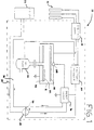
- Fig. 1 illustrates an exemplary semiconductor processing device 10.
- the devices can perform numerous manufacturing operations and include a semiconductor etcher device as shown in Fig. 1.
- Etching is but one example of a processing device which can utilize a cooling unit or system of the present invention.
- any processing device which uses an energy source can be retrofitted by the cooling unit hereof.
- Processing device 10 includes a wafer processing chamber 12, for example, a plasma etching chamber. Chamber 12 is coupled to receive gas from a gas supply 14 and power from an energy source 16.
- a gas control panel 18, generally fixed to the outer surface of processing device 10, allows the user to manually select a gas or a combination of gases to input into chamber 12.
- Gas control panel 18 and energy source 16 can be programmably controlled by an electronic controller 20.
- Controller 20 receives programmable input and, based upon that input, activates gas control panel 18 and energy source 16 to allow various types of gas and energy magnitude to be placed into and upon chamber 12.
- An exemplary processing device 10, such as a wafer autoetcher, can be obtained from LAM Research Corp. of Fremont, CA, model no. 490/590.
- the exemplary device, or autoetch device includes an RF power source operating at 100 watts to 1500 watts during normal plasma etch or reactive ion etch operation.
- the autoetcher also includes a gas control panel on the outer surface of the autoetcher which can allow the user to manually input a preferred etchant into the chamber.
- a suitable etchant includes a halogen species, various Freons ⁇ , and/or hydrogen/oxygen-based gases. Various other types of gases can also be used depending upon the semiconductor material to be etched.
- Energy source 16 operating at energies approaching 1500 watts, can oftentimes become heated to a level exceeding 100° C. Prolonged operation at high temperature may cause energy drift and inaccurate etching of wafer 22 placed within the chamber.
- Plasma which is generated between electrodes 24 and 26 of an exemplary etcher must be maintained within a close energy tolerance level.
- DC voltages from the RF generator is excluded by capacitive coupling the RF source to electrode 24. Any drift or stray in DC voltage may overcome the capacitor 28 causing intolerable damage to wafer 22. Any change whatsoever in the plasma energy level between electrodes 24 and 26 may also cause damage to wafer 22. Therefore, it becomes important that energy source 26, used in any type of processing device 10 including an etcher, be closely maintained to a specific operating temperature to optimize its output and prolong its lifetime.
- ions and free radicals generated in the plasma diffuse to electrode 26 and the surface of wafer 22 where they then react with the material being etched to form volatile products. The volatile products can then be quickly and easily evacuated or pumped away from wafer 22 via vacuum pump 30.
- a system necessary for cooling energy source 16 includes a chiller 32, first conduit 34, second conduit 36, and valve 38. Coolant is routed through first and second conduits 34 and 36 in the direction indicated by the arrows.
- Valve 38 is coupled to first conduit 34 to receive cooled coolant from chiller 32.
- Chiller 32 is of common design and utilizes either active or passive techniques for expelling heat from the coolant as the coolant is transferred over a heat or mass exchange surface.
- Freon ⁇ from gas supply 14 can be compressed and expanded, as in normal refrigeration, to cool coolant passed through chiller 32.
- Valve is activated by an electronic signal sent from electronic controller 20. Upon activation, valve 38 allows coolant in first conduit 34 to flow through the valve and into energy source 16. If valve 38 is deactivated, then it will route coolant from first conduit 34 to second conduit 36, via flow path 40, and back into chiller 32 as shown.
- valve 38 Whenever controller 20 produces electrical stimulus, generally during activation of energy source 16 or during programmable or manual generation, valve 38 will allow coolant flow into energy source 16. Conversely, whenever source 16 is deactivated or whenever the user manually or programmably desires, valve 38 will produce path 40 thereby bypassing or preventing coolant flow through source 16.
- Controller 20 may pre-exist within processing device 10.
- Controller 20 includes any controller which sends electronic stimulus to device 10 and/or energy source 16.
- Controller 20 can be a programmable controller and, for example, can also programmably and/or automatically control gas control panel 18 as well as vacuum pump 30 to achieve full automated processing.
- Controller 20 includes a digital input/output (DIO) circuit adapted to receive input from a programmable circuit or central processing unit (CPU) having, for example, an AT/XT IBM ⁇ -compatible bus architecture.
- a suitable DIO circuit can be obtained, for example, from Keithley Corp., Taunton MA, part no. PIO-12, having a programmable peripheral interface such as found in part no. 8255 obtained from Intel Corp., Santa Clara, CA.
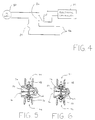
- An exemplary electronic controller 20 useable in an autoetcher manufactured by LAM Research Corp. is designated as having an output pin from the DIO denoted as "J3" to receive output signal to energy source 16. J3 pin can also be connected to valve 38 as shown in Fig. 1. It is appreciated, however, that any form of DIO circuit useable between a programmable device and a peripheral can be used to achieve the function of controller 20, and that J3 pinout of the LAM Research Corp. autoetcher is but only one example of the conductor point which can be tapped into and routed to a relay 82 (see Fig. 4) which controls valve 38.
- An exemplary autoetcher manufactured by LAM Research Corp. uses 24 V DC signals to actuate internal relays within the machine.
- Relay 82 is chosen to operate at 24 V DC as well, in order for a select signal sent over J3 pinout to interface directly to the relay. If an off-the-shelf controller using a DIO card described above is used, then the controller will typically operate at 5 V DC, and relay 82 is preferrably chosen having compatible 5 V DC operation. If necessary, the 24 V DC signals within the LAM autoetcher can be easily voltage divided to operate a 5 V controller and associated DIO card.
- Valve 38 can be configured to allow coolant to enter port 42 and exit either first output port 44 or second output port 46 (shown in dashed line to indicate its position on the opposing, non-visible side).
- Input port 42 receives coolant from first conduit 34 (shown in Fig. 1) and, depending upon the solenoid position, will output that coolant to first output port 44 or second output port 46.
- the first output port 44 can be connected to first conduit 34, while second output port 46 can be connected to second conduit 36 via flow path 40 (shown in Fig. 1).
- a suitable solenoid valve 38 can be obtained from Automatic Switch Co., Florham Park, NJ, part no. 8300D68RF.
- Valve 38 generally includes a mechanism which translates electrical energy applied to coil 48 into linear mechanical motion of armature or core 50.
- Core 50 moves within solenoid base 52 and against one end of valve lever 54.
- the entire coil and core assembly is contained within housing 56 and yoke 58, and is secured to valve body 62 via retaining cap 64.
- valve lever 54 Upon receipt of electrical input at conductor ends 66 of coil 48, valve lever 54 will pivot upward at the end nearest core 50. Downward movement of valve lever 54 will cause upper valve seat 68 to separate from valve body 62. Upward movement of valve lever 54 will cause separation of valve seat 68 from body 62 and allow a coolant flow path between input port 42 and one output port, preferably first output port 44.
- valve lever 54 Conversely, absence of an electrical input at conductor ends 66 will cause valve lever 54 to pivot downward in the direction of lateral biasing force exerted by upper spring 72.
- Upper spring 72 being of larger biasing force than lower spring 72, ensures valve seat 68 is not separated from valve body 62 absent electrical energy at conductor ends 66. Further, spring 72 ensures valve seat 70 is separated from valve body 62 whenever electrical energy is absent at conductor ends. Separation of seat 70 from body 62 provides coolant flow from input port 42 to second output port 46. Upper valve seat 68 will not open until lower valve seat 70 is closed, and vice versa.
- valve 38 The operation of valve 38 is fairly simple. Referring now to Fig. 5, an electrically inactive valve is shown. Valve lever 54 remains in a downward tilt about a pivot point 76 caused by biasing force of spring 72 (shown in Fig. 3).
- Spring 72 preferably includes a larger biasing force than spring 74. Spring 72, of larger axial biasing force than spring 74, ensures upper valve seat 68 is firmly and sealingly placed against the inner surface of valve body 62. Pressure by upper spring 72 also forces lower valve seat 70 to separate from valve body 62. Such separation allows coolant to flow from input port 42 to second output port 46.
- FIG. 6 an energized or electrically active valve is shown.
- coil 48 actuates core 50 causing connected valve lever 54 to tilt upward about pivot point 76.
- the electromagnetic force upon core 50 is sufficient to overcome the biasing force of upper spring 72.
- upper valve seat 68 is forced to separate from valve body 62. Separation or unseating of upper valve seat 68 allows fluid from input port 42 to flow to first output port 44 (shown in Fig. 2).
- Figs. 1, 2, 5 and 6 illustrate the routing of coolant from a first conduit and maintaining the routing through the first conduit during a first time period in which valve 38 is electrically activated (activation which causes input port of first conduit to be connected to first output port of first conduit).
- valve 38 Conversely, routing of coolant from first conduit to second conduit (bypassing source 16) occurs during a second time period in which valve 38 is electrically de-energized or inactive. Inactive valve 38 allows biasing spring 72 to open a flow path between input port 44 of first conduit to second output port 46 of second conduit.
- input conductors 66 of coil 48 are shown capable of receiving input from power supply 80.
- Power supply 80 is preferably an alternating current (AC) power supply and can be 120 volt AC.
- AC alternating current
- a suitable relay 82 can be a single pole, double throw relay manufactured by Magnecraft, Inc. of Northbrook, IL, part no. W388CQX-3.
- Relay 82 is activated by input from electronic controller 20. Whenever controller 20 generates an electrical output, relay 82 will cause direct connection between conductors 66 and power supply 80 provided fuse 84 is not blown.
- a suitable fuse can be a one ampere fuse of common design and structure.
- electronic controller 20 includes any controller associated with the electronic control of a processing device 10. Controller 20 emits electrical signals which can indicate activation and deactivation of energy source 16. Furthermore, controller 20 can be programmably manipulated to allow keyboard interface and cathode ray tube (CRT) monitoring of controller operation which includes any operation necessary to achieve wafer processing.
- CRT cathode ray tube
- An exemplary electronic controller is described hereinabove and useable in a LAM Research Corp. autoetcher model no. 490/590. However, various other types of electronic controllers can be used and fall within the scope of the present invention. As such, any controller which emits electronic signals indicative of energy source and/or processing device operation can be used to also emit the same signals to valve 38. Pre-existing hardware and software for processing equipment can be readily adapted and/or retrofitted to actuate the cooling unit of the present invention.
Landscapes
- Drying Of Semiconductors (AREA)
Description
Claims (13)
- A cooling unit for use with a semi-conductor processing device (12) operated by an energy generator (16) controlled by an electronic controller (20);
said cooling unit comprising a chiller (32), a pair of conduits (34,36) for conveying coolant coupled between the chiller (32) and the energy source (16) and a solenoid valve (38) coupled to the conduits (34,36) and controlled by the controller (20) to supply coolant from the chiller to the energy source (16) via one of the conduits (34,36) during a first time period during which the valve (38) is actuated by the controller (20) and when the energy source (16) is operating, so that the energy supplied by said energy generator is constant. - A coolant unit according to claim 1, wherein said semiconductor processing device (12) comprises a semiconductor etcher.
- A cooling unit according to claim 2, wherein said semiconductor etcher is a semiconductor plasma etcher.
- A cooling unit according to claim 1, 2 or 3 wherein said coolant is a fluid of high thermal conductivity.
- A cooling unit according to any one of claims 1 to 4, wherein said solenoid valve (38) is adapted to discharge said coolant into the other of said pair of conduits (36,34) during a second time period in which said valve is not actuated.
- A cooling unit according to claim 5, wherein the chiller (32) is provided with a mass transfer surface capable of expelling heat from said coolant; and the solenoid valve (38) has an input port (42) and first and second output ports (44,46), wherein said input port (42) is connected to said first conduit (34) to receive coolant directly from the chiller (32) said first output port (44) is connected to said first conduit (34) to feed coolant to the energy generator (16) and said second output port (46) is connected to said second conduit (36); and
the electronic controller (20) controls said solenoid valve to form a first path between said input port (42) and said first output port (44) during the first time period, and to form a second path between said input port (42) and said second output port (46) during the second time period. - A cooling unit according to any one of claims 1 to 6, wherein said solenoid valve (38) comprises:a helical conductive coil (48) extending along a central axis;a ferrous metal core (50) disposed along said central axis and capable of movement at least partially within said coil;a valve seat (68) indirectly connected to one end of said core; andcurrent means (66) connected to said coil for moving said valve seat to an open position.
- A cooling unit according to claim 7, wherein said solenoid valve (38) further comprises:
a spring (72) connected to said valve seat for biasing said valve seat to a closed position. - A cooling unit according to claim 8, wherein said conductive coil (48) is connected to said electronic controller (20).
- A cooling unit according to claim 7,8 or 9, wherein said open position allows said coolant to flow along said path formed between said input port (42) and said first output port (44).
- A cooling unit according to claim 7, 8 or 9, or 10 wherein said valve seat (68) adopts a closed position when the current means is inactive to allow said coolant to flow along said path formed between said input port (42) and said second output port (46).
- A cooling unit according to any one of claims 7 to 11, wherein said controller (20) comprises:a programmable circuit; anda digital input/output circuit adapted to programmably deliver said current means to said coil during said first time period.
- A semiconductor processing system comprising a processing device (12), an energy generator (16) operating the processing device (12), an electronic controller (20) for controlling the operation of the energy generator and a cooling unit according to any one of the preceding claims.
Applications Claiming Priority (2)
| Application Number | Priority Date | Filing Date | Title |
|---|---|---|---|
| US1603693A | 1993-02-10 | 1993-02-10 | |
| US16036 | 1993-02-10 |
Publications (2)
| Publication Number | Publication Date |
|---|---|
| EP0611052A1 EP0611052A1 (en) | 1994-08-17 |
| EP0611052B1 true EP0611052B1 (en) | 1998-11-04 |
Family
ID=21775037
Family Applications (1)
| Application Number | Title | Priority Date | Filing Date |
|---|---|---|---|
| EP94300470A Expired - Lifetime EP0611052B1 (en) | 1993-02-10 | 1994-01-21 | Apparatus for cooling semiconductor processing equipment |
Country Status (4)
| Country | Link |
|---|---|
| US (1) | US5709262A (en) |
| EP (1) | EP0611052B1 (en) |
| JP (1) | JPH06291086A (en) |
| DE (1) | DE69414281T2 (en) |
Families Citing this family (3)
| Publication number | Priority date | Publication date | Assignee | Title |
|---|---|---|---|---|
| US6026896A (en) * | 1997-04-10 | 2000-02-22 | Applied Materials, Inc. | Temperature control system for semiconductor processing facilities |
| US6889763B1 (en) * | 2000-10-23 | 2005-05-10 | Advanced Micro Devices, Inc. | System for rapidly and uniformly cooling resist |
| KR100456667B1 (en) * | 2001-11-01 | 2004-11-18 | 양청수 | High temperature plasma boiler |
Family Cites Families (3)
| Publication number | Priority date | Publication date | Assignee | Title |
|---|---|---|---|---|
| GB948295A (en) * | 1961-12-29 | 1964-01-29 | Burnett & Rolfe Ltd | Improvements relating to fluid control valves |
| US3310284A (en) * | 1964-08-20 | 1967-03-21 | Fujitsu Ltd | Hydraulic system rotary pilot valve |
| EP0399676A1 (en) * | 1989-05-01 | 1990-11-28 | Tegal Corporation | Dual temperature plasma etch |
-
1994
- 1994-01-21 EP EP94300470A patent/EP0611052B1/en not_active Expired - Lifetime
- 1994-01-21 DE DE69414281T patent/DE69414281T2/en not_active Expired - Fee Related
- 1994-02-09 JP JP6015029A patent/JPH06291086A/en not_active Withdrawn
- 1994-08-05 US US08/286,405 patent/US5709262A/en not_active Expired - Lifetime
Also Published As
| Publication number | Publication date |
|---|---|
| US5709262A (en) | 1998-01-20 |
| JPH06291086A (en) | 1994-10-18 |
| DE69414281T2 (en) | 1999-07-08 |
| DE69414281D1 (en) | 1998-12-10 |
| EP0611052A1 (en) | 1994-08-17 |
Similar Documents
| Publication | Publication Date | Title |
|---|---|---|
| US4969168A (en) | Wafer supporting apparatus | |
| US10804082B2 (en) | Substrate processing apparatus, and operation method for substrate processing apparatus | |
| US6604372B2 (en) | Air-conditioning system | |
| KR102475073B1 (en) | Substrate liquid processing apparatus, and control method of heater unit | |
| US8034181B2 (en) | Plasma processing apparatus | |
| KR101920821B1 (en) | Cleanroom air conditioner | |
| CN110275556B (en) | Temperature control method and system for electrostatic chuck and semiconductor processing equipment | |
| EP1047116A2 (en) | Backside gas delivery system for a semiconductor wafer processing system | |
| KR100508754B1 (en) | Temperature controller and etching apparatus having the same | |
| US5709262A (en) | Electronic valve for cooling semiconductor processing equipment | |
| US12278091B2 (en) | Substrate processing apparatus and substrate processing method | |
| JP2024500329A (en) | Isothermal ion source with auxiliary heater | |
| US20200211872A1 (en) | Temperature controlling apparatus and method of controlling the temperature controlling apparatus | |
| WO2005045877A1 (en) | Dual filament ion source | |
| US11229878B2 (en) | Dry air generation apparatus, dry air generation method, and substrate processing system | |
| US11692639B2 (en) | Valve device | |
| JP2005155983A (en) | Panel cooling system | |
| JP3932497B2 (en) | Two-way switching control valve | |
| US4143813A (en) | Air conditioning control and method of operation | |
| KR20170017506A (en) | Apparatus and method for treating a substrate | |
| KR950004153Y1 (en) | Cooling water supply detection circuit of ion implanter | |
| KR200141445Y1 (en) | Starting current control circuit of air conditioner | |
| USRE21510E (en) | Control mechanism | |
| JPH0498750A (en) | Ion implantation device | |
| KR100693876B1 (en) | Emergency Power Supply for Semiconductor Manufacturing Equipment |
Legal Events
| Date | Code | Title | Description |
|---|---|---|---|
| PUAI | Public reference made under article 153(3) epc to a published international application that has entered the european phase |
Free format text: ORIGINAL CODE: 0009012 |
|
| AK | Designated contracting states |
Kind code of ref document: A1 Designated state(s): BE DE DK ES FR GB GR IE IT LU NL PT SE |
|
| 17P | Request for examination filed |
Effective date: 19950119 |
|
| 17Q | First examination report despatched |
Effective date: 19961030 |
|
| GRAG | Despatch of communication of intention to grant |
Free format text: ORIGINAL CODE: EPIDOS AGRA |
|
| GRAG | Despatch of communication of intention to grant |
Free format text: ORIGINAL CODE: EPIDOS AGRA |
|
| GRAH | Despatch of communication of intention to grant a patent |
Free format text: ORIGINAL CODE: EPIDOS IGRA |
|
| GRAH | Despatch of communication of intention to grant a patent |
Free format text: ORIGINAL CODE: EPIDOS IGRA |
|
| GRAA | (expected) grant |
Free format text: ORIGINAL CODE: 0009210 |
|
| AK | Designated contracting states |
Kind code of ref document: B1 Designated state(s): BE DE DK ES FR GB GR IE IT LU NL PT SE |
|
| PG25 | Lapsed in a contracting state [announced via postgrant information from national office to epo] |
Ref country code: SE Free format text: THE PATENT HAS BEEN ANNULLED BY A DECISION OF A NATIONAL AUTHORITY Effective date: 19981104 Ref country code: NL Free format text: LAPSE BECAUSE OF FAILURE TO SUBMIT A TRANSLATION OF THE DESCRIPTION OR TO PAY THE FEE WITHIN THE PRESCRIBED TIME-LIMIT Effective date: 19981104 Ref country code: IT Free format text: LAPSE BECAUSE OF FAILURE TO SUBMIT A TRANSLATION OF THE DESCRIPTION OR TO PAY THE FEE WITHIN THE PRESCRIBED TIME-LIMIT;WARNING: LAPSES OF ITALIAN PATENTS WITH EFFECTIVE DATE BEFORE 2007 MAY HAVE OCCURRED AT ANY TIME BEFORE 2007. THE CORRECT EFFECTIVE DATE MAY BE DIFFERENT FROM THE ONE RECORDED. Effective date: 19981104 Ref country code: GR Free format text: LAPSE BECAUSE OF NON-PAYMENT OF DUE FEES Effective date: 19981104 Ref country code: ES Free format text: THE PATENT HAS BEEN ANNULLED BY A DECISION OF A NATIONAL AUTHORITY Effective date: 19981104 Ref country code: BE Free format text: LAPSE BECAUSE OF FAILURE TO SUBMIT A TRANSLATION OF THE DESCRIPTION OR TO PAY THE FEE WITHIN THE PRESCRIBED TIME-LIMIT Effective date: 19981104 |
|
| REF | Corresponds to: |
Ref document number: 69414281 Country of ref document: DE Date of ref document: 19981210 |
|
| ET | Fr: translation filed | ||
| REG | Reference to a national code |
Ref country code: IE Ref legal event code: FG4D |
|
| PG25 | Lapsed in a contracting state [announced via postgrant information from national office to epo] |
Ref country code: LU Free format text: LAPSE BECAUSE OF NON-PAYMENT OF DUE FEES Effective date: 19990121 Ref country code: IE Free format text: LAPSE BECAUSE OF NON-PAYMENT OF DUE FEES Effective date: 19990121 |
|
| PG25 | Lapsed in a contracting state [announced via postgrant information from national office to epo] |
Ref country code: PT Free format text: LAPSE BECAUSE OF FAILURE TO SUBMIT A TRANSLATION OF THE DESCRIPTION OR TO PAY THE FEE WITHIN THE PRESCRIBED TIME-LIMIT Effective date: 19990204 Ref country code: DK Free format text: LAPSE BECAUSE OF FAILURE TO SUBMIT A TRANSLATION OF THE DESCRIPTION OR TO PAY THE FEE WITHIN THE PRESCRIBED TIME-LIMIT Effective date: 19990204 |
|
| NLV1 | Nl: lapsed or annulled due to failure to fulfill the requirements of art. 29p and 29m of the patents act | ||
| PLBE | No opposition filed within time limit |
Free format text: ORIGINAL CODE: 0009261 |
|
| STAA | Information on the status of an ep patent application or granted ep patent |
Free format text: STATUS: NO OPPOSITION FILED WITHIN TIME LIMIT |
|
| 26N | No opposition filed | ||
| REG | Reference to a national code |
Ref country code: IE Ref legal event code: MM4A |
|
| PGFP | Annual fee paid to national office [announced via postgrant information from national office to epo] |
Ref country code: GB Payment date: 20011214 Year of fee payment: 9 |
|
| REG | Reference to a national code |
Ref country code: GB Ref legal event code: IF02 |
|
| PGFP | Annual fee paid to national office [announced via postgrant information from national office to epo] |
Ref country code: FR Payment date: 20020104 Year of fee payment: 9 |
|
| PGFP | Annual fee paid to national office [announced via postgrant information from national office to epo] |
Ref country code: DE Payment date: 20020131 Year of fee payment: 9 |
|
| PG25 | Lapsed in a contracting state [announced via postgrant information from national office to epo] |
Ref country code: GB Free format text: LAPSE BECAUSE OF NON-PAYMENT OF DUE FEES Effective date: 20030121 |
|
| PG25 | Lapsed in a contracting state [announced via postgrant information from national office to epo] |
Ref country code: DE Free format text: LAPSE BECAUSE OF NON-PAYMENT OF DUE FEES Effective date: 20030801 |
|
| GBPC | Gb: european patent ceased through non-payment of renewal fee | ||
| PG25 | Lapsed in a contracting state [announced via postgrant information from national office to epo] |
Ref country code: FR Free format text: LAPSE BECAUSE OF NON-PAYMENT OF DUE FEES Effective date: 20030930 |
|
| REG | Reference to a national code |
Ref country code: FR Ref legal event code: ST |