EP0610631A1 - Electrical connector - Google Patents
Electrical connector Download PDFInfo
- Publication number
- EP0610631A1 EP0610631A1 EP93310547A EP93310547A EP0610631A1 EP 0610631 A1 EP0610631 A1 EP 0610631A1 EP 93310547 A EP93310547 A EP 93310547A EP 93310547 A EP93310547 A EP 93310547A EP 0610631 A1 EP0610631 A1 EP 0610631A1
- Authority
- EP
- European Patent Office
- Prior art keywords
- module
- pads
- base
- integrated circuit
- pins
- Prior art date
- Legal status (The legal status is an assumption and is not a legal conclusion. Google has not performed a legal analysis and makes no representation as to the accuracy of the status listed.)
- Withdrawn
Links
Images


Classifications
-
- H—ELECTRICITY
- H05—ELECTRIC TECHNIQUES NOT OTHERWISE PROVIDED FOR
- H05K—PRINTED CIRCUITS; CASINGS OR CONSTRUCTIONAL DETAILS OF ELECTRIC APPARATUS; MANUFACTURE OF ASSEMBLAGES OF ELECTRICAL COMPONENTS
- H05K1/00—Printed circuits
- H05K1/02—Details
- H05K1/14—Structural association of two or more printed circuits
- H05K1/141—One or more single auxiliary printed circuits mounted on a main printed circuit, e.g. modules, adapters
-
- H—ELECTRICITY
- H01—ELECTRIC ELEMENTS
- H01L—SEMICONDUCTOR DEVICES NOT COVERED BY CLASS H10
- H01L23/00—Details of semiconductor or other solid state devices
- H01L23/48—Arrangements for conducting electric current to or from the solid state body in operation, e.g. leads, terminal arrangements ; Selection of materials therefor
- H01L23/488—Arrangements for conducting electric current to or from the solid state body in operation, e.g. leads, terminal arrangements ; Selection of materials therefor consisting of soldered or bonded constructions
- H01L23/498—Leads, i.e. metallisations or lead-frames on insulating substrates, e.g. chip carriers
- H01L23/49827—Via connections through the substrates, e.g. pins going through the substrate, coaxial cables
-
- H—ELECTRICITY
- H05—ELECTRIC TECHNIQUES NOT OTHERWISE PROVIDED FOR
- H05K—PRINTED CIRCUITS; CASINGS OR CONSTRUCTIONAL DETAILS OF ELECTRIC APPARATUS; MANUFACTURE OF ASSEMBLAGES OF ELECTRICAL COMPONENTS
- H05K1/00—Printed circuits
- H05K1/02—Details
- H05K1/0286—Programmable, customizable or modifiable circuits
- H05K1/0287—Programmable, customizable or modifiable circuits having an universal lay-out, e.g. pad or land grid patterns or mesh patterns
- H05K1/0289—Programmable, customizable or modifiable circuits having an universal lay-out, e.g. pad or land grid patterns or mesh patterns having a matrix lay-out, i.e. having selectively interconnectable sets of X-conductors and Y-conductors in different planes
-
- H—ELECTRICITY
- H01—ELECTRIC ELEMENTS
- H01L—SEMICONDUCTOR DEVICES NOT COVERED BY CLASS H10
- H01L2924/00—Indexing scheme for arrangements or methods for connecting or disconnecting semiconductor or solid-state bodies as covered by H01L24/00
- H01L2924/0001—Technical content checked by a classifier
- H01L2924/0002—Not covered by any one of groups H01L24/00, H01L24/00 and H01L2224/00
-
- H—ELECTRICITY
- H01—ELECTRIC ELEMENTS
- H01L—SEMICONDUCTOR DEVICES NOT COVERED BY CLASS H10
- H01L2924/00—Indexing scheme for arrangements or methods for connecting or disconnecting semiconductor or solid-state bodies as covered by H01L24/00
- H01L2924/095—Indexing scheme for arrangements or methods for connecting or disconnecting semiconductor or solid-state bodies as covered by H01L24/00 with a principal constituent of the material being a combination of two or more materials provided in the groups H01L2924/013 - H01L2924/0715
- H01L2924/097—Glass-ceramics, e.g. devitrified glass
- H01L2924/09701—Low temperature co-fired ceramic [LTCC]
-
- H—ELECTRICITY
- H05—ELECTRIC TECHNIQUES NOT OTHERWISE PROVIDED FOR
- H05K—PRINTED CIRCUITS; CASINGS OR CONSTRUCTIONAL DETAILS OF ELECTRIC APPARATUS; MANUFACTURE OF ASSEMBLAGES OF ELECTRICAL COMPONENTS
- H05K2201/00—Indexing scheme relating to printed circuits covered by H05K1/00
- H05K2201/04—Assemblies of printed circuits
- H05K2201/049—PCB for one component, e.g. for mounting onto mother PCB
-
- H—ELECTRICITY
- H05—ELECTRIC TECHNIQUES NOT OTHERWISE PROVIDED FOR
- H05K—PRINTED CIRCUITS; CASINGS OR CONSTRUCTIONAL DETAILS OF ELECTRIC APPARATUS; MANUFACTURE OF ASSEMBLAGES OF ELECTRICAL COMPONENTS
- H05K2201/00—Indexing scheme relating to printed circuits covered by H05K1/00
- H05K2201/09—Shape and layout
- H05K2201/09818—Shape or layout details not covered by a single group of H05K2201/09009 - H05K2201/09809
- H05K2201/09945—Universal aspects, e.g. universal inner layers or via grid, or anisotropic interposer
-
- H—ELECTRICITY
- H05—ELECTRIC TECHNIQUES NOT OTHERWISE PROVIDED FOR
- H05K—PRINTED CIRCUITS; CASINGS OR CONSTRUCTIONAL DETAILS OF ELECTRIC APPARATUS; MANUFACTURE OF ASSEMBLAGES OF ELECTRICAL COMPONENTS
- H05K2201/00—Indexing scheme relating to printed circuits covered by H05K1/00
- H05K2201/10—Details of components or other objects attached to or integrated in a printed circuit board
- H05K2201/10227—Other objects, e.g. metallic pieces
- H05K2201/10325—Sockets, i.e. female type connectors comprising metallic connector elements integrated in, or bonded to a common dielectric support
-
- H—ELECTRICITY
- H05—ELECTRIC TECHNIQUES NOT OTHERWISE PROVIDED FOR
- H05K—PRINTED CIRCUITS; CASINGS OR CONSTRUCTIONAL DETAILS OF ELECTRIC APPARATUS; MANUFACTURE OF ASSEMBLAGES OF ELECTRICAL COMPONENTS
- H05K2201/00—Indexing scheme relating to printed circuits covered by H05K1/00
- H05K2201/10—Details of components or other objects attached to or integrated in a printed circuit board
- H05K2201/10613—Details of electrical connections of non-printed components, e.g. special leads
- H05K2201/10621—Components characterised by their electrical contacts
- H05K2201/10689—Leaded Integrated Circuit [IC] package, e.g. dual-in-line [DIL]
-
- H—ELECTRICITY
- H05—ELECTRIC TECHNIQUES NOT OTHERWISE PROVIDED FOR
- H05K—PRINTED CIRCUITS; CASINGS OR CONSTRUCTIONAL DETAILS OF ELECTRIC APPARATUS; MANUFACTURE OF ASSEMBLAGES OF ELECTRICAL COMPONENTS
- H05K2201/00—Indexing scheme relating to printed circuits covered by H05K1/00
- H05K2201/10—Details of components or other objects attached to or integrated in a printed circuit board
- H05K2201/10613—Details of electrical connections of non-printed components, e.g. special leads
- H05K2201/10621—Components characterised by their electrical contacts
- H05K2201/10704—Pin grid array [PGA]
-
- H—ELECTRICITY
- H05—ELECTRIC TECHNIQUES NOT OTHERWISE PROVIDED FOR
- H05K—PRINTED CIRCUITS; CASINGS OR CONSTRUCTIONAL DETAILS OF ELECTRIC APPARATUS; MANUFACTURE OF ASSEMBLAGES OF ELECTRICAL COMPONENTS
- H05K3/00—Apparatus or processes for manufacturing printed circuits
- H05K3/46—Manufacturing multilayer circuits
- H05K3/4602—Manufacturing multilayer circuits characterized by a special circuit board as base or central core whereon additional circuit layers are built or additional circuit boards are laminated
Definitions
- This invention relates to electrical connectors of the kind for connecting an integrated circuit to a receptacle such as a socket.
- the invention also relates to a method of manufacturing such an electrical connector.
- Multi-Chip Module One type of such an electrical connector is a Multi-Chip Module (MCM).
- MCMs Multi-Chip Modules
- MCMs are generally constructed from stacks of sheets of thin ceramic material, which are termed "green tape ceramic" because of their appearance.
- green tape ceramic A simplified sequence of the construction is the following:
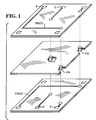
- connection formed is shown schematically in Figure 1.
- the TRACES cross over each other, by means of the VIAs: pad A connects with pad B, pad C with D, and so on.
- the traces form a 3-dimensional network, which is sometimes termed a "non-planar" network.
- the 3-dimensional network connects integrated circuits (not shown) with each other and with other connectors.
- MCMs have numerous advantages, but also have limitations.
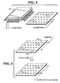
- One limitation is that the spacing between the holes (which contain the vias) is limited to about 200 microns, as indicated in Figure 2.
- a second problem is that the MCM experiences random size changes during the firing process.
- the MCM shrinks during firing about 15 or 20 percent, and each (shrunken) part varies from its fellow parts by 0.5 %: a size variation ranging from - 0.5 % to + 0.5 % occurs.
- MCMs Another feature of MCMs is their cost. In large production runs, they can be quite inexpensive, because the cost of equipment, such as the die which punches the holes, can be amortized over thousands of MCMs produced. However, for small production runs, in the tens or hundreds, the amortized cost per MCM produced becomes prohibitively high.
- a connector for connecting an integrated circuit to a receptacle characterized by a base module have connector pins adapted to connect with said receptacle, said connector pins being electrically coupled by first coupling means to base pads provided on said base module; and an integrated circuit module having IC pads thereon adapted to contact IC pins provided on an integrated circuit, said IC pads being electrically coupled by second coupling means to further pads provided on said IC module which are larger than, and adapted to mate with respective base pads.
- a method of manufacturing an electrical connector characterized by the steps of: selecting a base module which includes an array of base pads, an array of connector pins and conductive leads coupling said connector pins to said base pads; and forming an integrated circuit module on said base module by forming a plurality of layers each having a plurality of conductive traces thereon and holes for vias therein, said IC module having further pads thereon which are larger than and mate with respective base pads, and also having IC pads thereon for contact pins provided on an integrated circuit.
- Figure 1 illustrates, in simplified schematic form, a three-dimensional network used in multi-chip modules.
- Figure 2 illustrates an integrated circuit (IC) having a pin spacing of 100 microns and a pad spacing of 200 microns.
- Figure 3 illustrates shrinkage or expansion which can occur during firing of a multi-chip module.
- Figure 4A illustrates, in x-ray view, a simplified form of the invention.
- Figure 4B illustrates, in unfolded view, three of the components of Figure 4A. Parts of Figure 4B are shown in Figures 5 and 6.
- Figure 5 illustrates internal features of the BASE MODULE and the IC MODULE of Figure 4A.
- Figure 6 illustrates how the IC LAYER mates to the IC MODULE.
- Figures 7A and 7B illustrate the mismatch which can occur between the BASE PADs and the OVERLAPPING PADs of Figure 5.
- Figure 8 illustrates how VIAs penetrate metal film layers in the IC MODULE.
- Figure 9 illustrates formation of METAL TRACES.
- Figure 10 shows a sheet of BASE MODULEs.
- Figure 11 shows an IC MODULE carrying edge-connectors.
- Figure 12 shows a cross-section of Figure 11.
- a simplified, X-ray view of one form of the invention is shown in Figure 4A.
- a BASE MODULE contains PINs for connection with a receptacle such as a socket (not shown).
- the BASE MODULE carries an IC MODULE, which, in turn, carries an integrated circuit, IC.
- Each PIN of the BASE MODULE connects with an IC PAD by way of a CONDUCTOR, shown dashed.
- the BASE MODULE is a ceramic MCM. In practice, only a few BASE MODULES, each with a somewhat different routing pattern, are manufactured, because of their high cost.
- a BASE MODULE having a proper routing pattern of CONDUCTORs is selected from a collection of BASE MODULEs.
- an IC MODULE is manufactured to accommodate the particular IC and the particular IC PAD-to-IC PIN connection desired. The IC MODULE is manufactured upon the BASE MODULE.
- the IC MODULE is constructed of layers of polyimide material onto which conductive traces are formed using integrated circuit fabrication techniques.
- Figure 4B shows the connector of Figure 4A, but in an unfolded configuration which corresponds to the configurations shown in Figures 5 and 6.
- the unfolded configuration is used in order to show internal connections.
- the IC MODULE is preferably not constructed as a separate element, which is then bonded to the BASE MODULE, but is manufactured upon the BASE MODULE, layer-by-layer.
- the PINs connect to BASE PADs by way of CONDUCTORs indicated by dashed lines.
- the BASE PADs are actually the ends of the vias which act as plugs within the holes in the CERAMIC SHEET.
- the CONDUCTORs shown make direct connections between the BASE PADs and the PINs: each CONDUCTOR follows a straight vertical path from a PIN to a BASE PAD. With this configuration, the ROUTING LAYERs may not be necessary, and can be omitted. (The ROUTING LAYERs perform the function shown in Figure 1: a selected PIN can be connected to a selected BASE PAD. Only three paths are shown for simplicity, but, in practice, hundreds, or thousands, of paths can be used.)
- Layers 3 and 6 contain parallel conductors which act as power lines: on each layer, these conductors are all held at the same electrical potential. For example, layer 6 can be held at Vdd, and layer 3 at Vss. The conductors on layer 6 are orthogonal to those on layer 3. These layers carry power for the integrated circuits which will be carried by the IC MODULE. Layers 3 and 6 are not strictly necessary, and can be omitted in some situations.
- the IC MODULE contains a network of CONDUCTORs and VIAs, shown in simplified form in Figure 6.
- the CONDUCTORs make contact with the BASE PADs (on the BASE MODULE) by means of OVERLAPPING PADS, shown in Figures 5 and 6.
- OVERLAPPING PADs are larger than the BASE PADs, to accommodate the expansion and shrinkage, discussed hereinabove, which occurs in the BASE MODULE.
- the BASE PADs in Figure 5 are 203 microns (8 mils) in diameter, while the OVERLAPPING PADs are 762 microns (30 mils) in diameter.
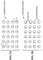
- Figure 7A the BASE MODULE expands by 0.5 percent.
- One OVERLAPPING PAD 12 (the larger circle) is centered on a BASE PAD 10. The rest are progressively off-center, and the maximal degree of off-centering occurs at the pair of pads 15 and 18 which is farthest from the centered pads 10 and 12. Thus, despite the expansion, all pairs of pads make good contact.
- the OVERLAPPING PADs in Figure 6 are connected, by a three-dimensional network of VIAs and CONDUCTORs (or traces), to IC PADs on an IC layer.
- the VIAs penetrate, without contacting, two power planes, as shown in Figure 8. One plane is carried by layer 20, and the other is carried by layer 25.
- the VIAs which form part of the network, do not contact the METAL FILM which forms the power planes.
- the VIAs pass through holes in the film, without making contact.
- One METAL FILM is held at a high potential, such as Vdd, and the other METAL FILM is held at a low potential, such as Vss.
- the layers forming the IC MODULE in Figure 5 are preferably a polyimide polymer, of typical thickness 10 - 25 microns.
- the polyimide layers are constructed by spinning the BASE MODULE on a centrifuge, and applying a liquid precursor, which centrifugal force spreads out into a thin layer. Upon curing, the thin layer becomes a polyimide layer.
- the CONDUCTORs (also called traces) in Figure 6 on the layers are formed using standard integrated circuit fabrication techniques.
- a layer of POLYIMIDE bearing a METAL FILM (preferably nickel), typically 1,000 Angstroms thick, provides an initial working material.
- PHOTORESIST is applied to the METAL FILM.
- An IMAGE is created on the PHOTORESIST, such as by contact printing or use of a projector.
- the PHOTORESIST is developed, as indicated, which leaves hardened PHOTORESIST at places where the METAL FILM is to be protected from etching.
- the structure is subjected to an etchant, which removes the METAL FILM which is unprotected by the PHOTORESIST, leaving a pattern of METAL TRACES, as shown.
- the remaining, hardened, photoresist is removed from the METAL TRACES.
- METAL TRACES in Figure 9 can be desirable.
- a layer of copper preferably about 5 to 10 microns thick, is plated onto the METAL TRACES.
- another layer preferably nickel, is plated onto the copper.
- the METAL TRACES thus become tri-layered: they contain three layers of metal. Such plating is known in the art. This plating increases the effective thickness of the METAL TRACES, allowing the plated traces to carry more current.
- the plating is done to increase thickness, rather than attempting to produce thick METAL TRACEs initially, because it is difficult to etch thick METAL TRACES from a thick METAL FILM (in the range of between 5 and 10 microns). Further, it is difficult to etch small line widths in copper, but easier to plate existing lines using copper.
- the second layer of nickel is applied to isolate the copper from the polyimide. If moisture should contact the polyimide in the presence of the copper, then corrosion can occur.
- the IC LAYER in Figure 6 can contain IC PADs having a spacing smaller than the spacing between the BASE PADs in Figure 5.
- BASE PADs are actually the tops of tungsten vias. These vias reside in the punched holes which were previously punched in the green ceramic tape during manufacture of the BASE MODULE. As stated above, the minimum spacing between the punched holes is typically limited to about 200 microns, as shown in Figure 2.
- the spacing of the IC PADs in Figure 6 is limited by the fabrication technique used, which is different from that which limits the BASE PAD spacing.
- pad spacings of 50 microns (as opposed to 300 microns for the BASE PADs) can be attained using integrated circuit fabrication techniques.
- Prior-art technology used in manufacturing integrated circuits is capable of producing line widths W in Figure 9 of 10 microns, or less.
- This same technology can produce spacings S of 10 microns, or less. These spacings are less than twenty percent of the 300-micron spacing shown in Figure 2, which exists between the BASE PADs in the BASE MODULE.
- One useful combination of spacings is 300 microns for the BASE PADs in Figure 5, and 100 microns for the IC PADs in Figure 6.
- the 203 micron (8-mil) vias are preferably on 305 micron (12-mil) centers.
- VIAs in Figure 6 in the IC MODULE are produced by masking and etching, as known in the integrated circuit fabrication art.
- the BASE MODULES shown in Figure 5, can be manufactured in large sheets, such as shown in Figure 10. Each module in the sheet has a connection pattern between its pins (concealed from view in Figure 10, but shown in Figure 5) and the BASE PADs (shown in Figure 10). For ease of manufacture, all BASE MODULES on a given sheet will have the same connection configuration.
- edge connectors can be used, as shown in Figure 11.
- a cross section is shown in Figure 12.
- the layers in the cross section are polyimide sheet.
- the top polyimide sheet can carry the edge-card traces shown in Figure 11.
- OVERLAPPING PADs in Figure 5 overlap the BASE PADs, not each other.
- the OVERLAPPING PADs may also be called "over-size" pads, because their cross-sectional areas exceed the minimal area necessary to carry the required current.
- the BASE PADs have at least this minimal area, and they are smaller than the oversize pads.
- the center-to-center spacing between the BASE PADs in Figure 5 is also called their "pitch.”
- the pitch shown in Figure 2 is a minimum of 300 microns.
- the pitch for the IC pins in that Figure is 100 microns.
- the pitch of the BASE PADs can vary from 99.5% to 100.5% of the desired pitch.
- the BASE PAD pitch can thus be termed "random.” It contains "random error.” This does not mean that the pitch cannot be known: it can be ascertained by measurement. This does, however, mean that the pitch is not known in advance. That is, even if the pitch is known prior to firing of BASE PADs, nevertheless, after firing, the pitch becomes indeterminate.
- TAB in Figure 13 refers to the standard Tape Automated Bonding technique used to attach the IC to the TAB frame.
- the TAB frame is welded to the IC pads using thermosonic bonding.
- the top surface of the IC MODULE is gold-plated, to facilitate the thermosonic bonding, and for oxidation resistance.
Applications Claiming Priority (2)
| Application Number | Priority Date | Filing Date | Title |
|---|---|---|---|
| US99699192A | 1992-12-28 | 1992-12-28 | |
| US996991 | 1992-12-28 |
Publications (1)
| Publication Number | Publication Date |
|---|---|
| EP0610631A1 true EP0610631A1 (en) | 1994-08-17 |
Family
ID=25543525
Family Applications (1)
| Application Number | Title | Priority Date | Filing Date |
|---|---|---|---|
| EP93310547A Withdrawn EP0610631A1 (en) | 1992-12-28 | 1993-12-24 | Electrical connector |
Country Status (2)
| Country | Link |
|---|---|
| EP (1) | EP0610631A1 (ja) |
| JP (1) | JPH06232335A (ja) |
Cited By (5)
| Publication number | Priority date | Publication date | Assignee | Title |
|---|---|---|---|---|
| EP0792517A1 (en) * | 1994-11-15 | 1997-09-03 | Formfactor, Inc. | Electrical contact structures from flexible wire |
| US6336269B1 (en) | 1993-11-16 | 2002-01-08 | Benjamin N. Eldridge | Method of fabricating an interconnection element |
| US6727579B1 (en) | 1994-11-16 | 2004-04-27 | Formfactor, Inc. | Electrical contact structures formed by configuring a flexible wire to have a springable shape and overcoating the wire with at least one layer of a resilient conductive material, methods of mounting the contact structures to electronic components, and applications for employing the contact structures |
| US6778406B2 (en) | 1993-11-16 | 2004-08-17 | Formfactor, Inc. | Resilient contact structures for interconnecting electronic devices |
| US8485418B2 (en) | 1995-05-26 | 2013-07-16 | Formfactor, Inc. | Method of wirebonding that utilizes a gas flow within a capillary from which a wire is played out |
Citations (4)
| Publication number | Priority date | Publication date | Assignee | Title |
|---|---|---|---|---|
| FR2567684A1 (fr) * | 1984-07-10 | 1986-01-17 | Nec Corp | Module ayant un substrat ceramique multicouche et un circuit multicouche sur ce substrat et procede pour sa fabrication |
| FR2601501A1 (fr) * | 1986-07-14 | 1988-01-15 | Nec Corp | Substrat conducteur multicouche |
| FR2611412A1 (fr) * | 1987-02-26 | 1988-09-02 | Nec Corp | Carte stratifiee d'interconnexion |
| EP0465138A2 (en) * | 1990-06-29 | 1992-01-08 | General Electric Company | Interconnection of electronic components |
-
1993
- 1993-12-24 EP EP93310547A patent/EP0610631A1/en not_active Withdrawn
- 1993-12-27 JP JP34726593A patent/JPH06232335A/ja active Pending
Patent Citations (4)
| Publication number | Priority date | Publication date | Assignee | Title |
|---|---|---|---|---|
| FR2567684A1 (fr) * | 1984-07-10 | 1986-01-17 | Nec Corp | Module ayant un substrat ceramique multicouche et un circuit multicouche sur ce substrat et procede pour sa fabrication |
| FR2601501A1 (fr) * | 1986-07-14 | 1988-01-15 | Nec Corp | Substrat conducteur multicouche |
| FR2611412A1 (fr) * | 1987-02-26 | 1988-09-02 | Nec Corp | Carte stratifiee d'interconnexion |
| EP0465138A2 (en) * | 1990-06-29 | 1992-01-08 | General Electric Company | Interconnection of electronic components |
Cited By (8)
| Publication number | Priority date | Publication date | Assignee | Title |
|---|---|---|---|---|
| US6336269B1 (en) | 1993-11-16 | 2002-01-08 | Benjamin N. Eldridge | Method of fabricating an interconnection element |
| US6778406B2 (en) | 1993-11-16 | 2004-08-17 | Formfactor, Inc. | Resilient contact structures for interconnecting electronic devices |
| US6835898B2 (en) | 1993-11-16 | 2004-12-28 | Formfactor, Inc. | Electrical contact structures formed by configuring a flexible wire to have a springable shape and overcoating the wire with at least one layer of a resilient conductive material, methods of mounting the contact structures to electronic components, and applications for employing the contact structures |
| US7225538B2 (en) | 1993-11-16 | 2007-06-05 | Formfactor, Inc. | Resilient contact structures formed and then attached to a substrate |
| EP0792517A1 (en) * | 1994-11-15 | 1997-09-03 | Formfactor, Inc. | Electrical contact structures from flexible wire |
| EP0792517A4 (en) * | 1994-11-15 | 1998-06-24 | Formfactor Inc | ELECTRIC CONTACT STRUCTURES OBTAINED BY CONFIGURATION OF A FLEXIBLE WIRE |
| US6727579B1 (en) | 1994-11-16 | 2004-04-27 | Formfactor, Inc. | Electrical contact structures formed by configuring a flexible wire to have a springable shape and overcoating the wire with at least one layer of a resilient conductive material, methods of mounting the contact structures to electronic components, and applications for employing the contact structures |
| US8485418B2 (en) | 1995-05-26 | 2013-07-16 | Formfactor, Inc. | Method of wirebonding that utilizes a gas flow within a capillary from which a wire is played out |
Also Published As
| Publication number | Publication date |
|---|---|
| JPH06232335A (ja) | 1994-08-19 |
Similar Documents
| Publication | Publication Date | Title |
|---|---|---|
| EP0469308B1 (en) | Multilayered circuit board assembly and method of making same | |
| EP0764352B1 (en) | Microelectronic contacts and assemblies | |
| US7312103B1 (en) | Method for making an integrated circuit substrate having laser-embedded conductive patterns | |
| US5786270A (en) | Method of forming raised metallic contacts on electrical circuits for permanent bonding | |
| US5686702A (en) | Polyimide multilayer wiring substrate | |
| US7874065B2 (en) | Process for making a multilayer circuit board | |
| US3932932A (en) | Method of making multilayer printed circuit board | |
| US5774340A (en) | Planar redistribution structure and printed wiring device | |
| EP0365755B1 (en) | Circuit member for use in multilayered printed circuit board assembly and method of making same | |
| US9170274B2 (en) | Wiring board for electronic parts inspecting device and its manufacturing method | |
| JP4597631B2 (ja) | 部品内蔵配線板、部品内蔵配線板の製造方法 | |
| DE69723801T2 (de) | Herstellungsverfahren einer Kontaktgitter-Halbleiterpackung | |
| US4107836A (en) | Circuit board with self-locking terminals | |
| US4187388A (en) | Circuit board with self-locking terminals | |
| EP0610631A1 (en) | Electrical connector | |
| US8981237B2 (en) | Wiring board for electronic parts inspecting device and its manufacturing method | |
| EP0332747B1 (en) | Tape automated bonding package | |
| US20010039727A1 (en) | Manufacturing method for multilayer printed circuit board | |
| JP2623980B2 (ja) | 半導体搭載用リード付き基板の製造法 | |
| US20220361329A1 (en) | Method for Forming Flipped-Conductor-Patch | |
| KR100271793B1 (ko) | 다층인쇄회로기판의층간배선연결방법 | |
| EP0857403B1 (en) | Method of forming raised metallic contacts on electrical circuits for permanent bonding | |
| EP0525217A1 (en) | Carrier for electronic components | |
| JP3045593B2 (ja) | 複数の芯導体を有する層間接続体付き配線板 | |
| JP2012099591A (ja) | 電子部品検査用配線基板およびその製造方法 |
Legal Events
| Date | Code | Title | Description |
|---|---|---|---|
| PUAI | Public reference made under article 153(3) epc to a published international application that has entered the european phase |
Free format text: ORIGINAL CODE: 0009012 |
|
| AK | Designated contracting states |
Kind code of ref document: A1 Designated state(s): DE FR GB |
|
| RAP1 | Party data changed (applicant data changed or rights of an application transferred) |
Owner name: AT&T GLOBAL INFORMATION SOLUTIONS INTERNATIONAL IN |
|
| 17P | Request for examination filed |
Effective date: 19950211 |
|
| RAP1 | Party data changed (applicant data changed or rights of an application transferred) |
Owner name: HYUNDAI ELECTRONICS AMERICA |
|
| RAP1 | Party data changed (applicant data changed or rights of an application transferred) |
Owner name: HYUNDAI ELECTRONICS AMERICA Owner name: AT&T GLOBAL INFORMATION SOLUTIONS INTERNATIONAL IN |
|
| RAP1 | Party data changed (applicant data changed or rights of an application transferred) |
Owner name: SYMBIOS LOGIC INC. Owner name: HYUNDAI ELECTRONICS AMERICA Owner name: AT&T GLOBAL INFORMATION SOLUTIONS INTERNATIONAL IN |
|
| RAP1 | Party data changed (applicant data changed or rights of an application transferred) |
Owner name: SYMBIOS LOGIC INC. Owner name: HYUNDAI ELECTRONICS AMERICA Owner name: NCR INTERNATIONAL, INC. |
|
| 17Q | First examination report despatched |
Effective date: 19970513 |
|
| RAP1 | Party data changed (applicant data changed or rights of an application transferred) |
Owner name: SYMBIOS, INC. Owner name: HYUNDAI ELECTRONICS AMERICA Owner name: NCR INTERNATIONAL, INC. |
|
| STAA | Information on the status of an ep patent application or granted ep patent |
Free format text: STATUS: THE APPLICATION IS DEEMED TO BE WITHDRAWN |
|
| 18D | Application deemed to be withdrawn |
Effective date: 19980123 |