EP0602909A2 - SIMD-Architektur mit einem Bus zur Datenübertragung von und zu Verarbeitungseinheiten - Google Patents
SIMD-Architektur mit einem Bus zur Datenübertragung von und zu Verarbeitungseinheiten Download PDFInfo
- Publication number
- EP0602909A2 EP0602909A2 EP93309971A EP93309971A EP0602909A2 EP 0602909 A2 EP0602909 A2 EP 0602909A2 EP 93309971 A EP93309971 A EP 93309971A EP 93309971 A EP93309971 A EP 93309971A EP 0602909 A2 EP0602909 A2 EP 0602909A2
- Authority
- EP
- European Patent Office
- Prior art keywords
- circuitry
- data
- bus
- processing unit
- processing units
- Prior art date
- Legal status (The legal status is an assumption and is not a legal conclusion. Google has not performed a legal analysis and makes no representation as to the accuracy of the status listed.)
- Granted
Links
Images


Classifications
-
- G—PHYSICS
- G06—COMPUTING; CALCULATING OR COUNTING
- G06F—ELECTRIC DIGITAL DATA PROCESSING
- G06F15/00—Digital computers in general; Data processing equipment in general
- G06F15/16—Combinations of two or more digital computers each having at least an arithmetic unit, a program unit and a register, e.g. for a simultaneous processing of several programs
- G06F15/163—Interprocessor communication
- G06F15/173—Interprocessor communication using an interconnection network, e.g. matrix, shuffle, pyramid, star, snowflake
- G06F15/17356—Indirect interconnection networks
- G06F15/17368—Indirect interconnection networks non hierarchical topologies
-
- G—PHYSICS
- G06—COMPUTING; CALCULATING OR COUNTING
- G06F—ELECTRIC DIGITAL DATA PROCESSING
- G06F15/00—Digital computers in general; Data processing equipment in general
- G06F15/76—Architectures of general purpose stored program computers
- G06F15/80—Architectures of general purpose stored program computers comprising an array of processing units with common control, e.g. single instruction multiple data processors
- G06F15/8007—Architectures of general purpose stored program computers comprising an array of processing units with common control, e.g. single instruction multiple data processors single instruction multiple data [SIMD] multiprocessors
- G06F15/8015—One dimensional arrays, e.g. rings, linear arrays, buses
Definitions
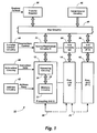
- Figs. 1-2C illustrate general features of the invention.
- Fig. 1 shows circuitry for transferring items of data to and from processing units in a SIMD parallel processor.
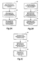
- Figs. 2A-2C show general acts in data transfers using circuitry like that of Fig. 1.
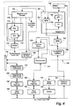
- DVMA interface 112 a master interface, and slave interface 114 can be implemented in accordance with SBus Specification B.0, Sun Microsystems, Inc. Part No. 800-5922-10, 1990, which describes signal protocols for SBus master and slave interfaces. Each interface can have a respective sequencer.
- card 110 includes a number of components that provide signals to components in box 120 or receive signals from components in box 120, thus performing functions of DVMA interface 112 or slave interface 114.
- Box 120 also includes power supply 140, which can be a conventional power supply capable of providing approximately 40 amps at 5 volts, or 200 watts. Box 120 also contains a cooling fan (not shown).
- power supply 140 can be a conventional power supply capable of providing approximately 40 amps at 5 volts, or 200 watts. Box 120 also contains a cooling fan (not shown).
- Control/status register 168 is a conventional register whose most significant bit, called the RUN bit, indicates whether sequencer 160 shou!d perform normal addressing or should provide a special address that holds the coprocessor.
- the IDT49C410 sequencer has a JumpZero instruction to which it responds by providing the address of location 0 to MAR 152. Therefore, the special address can be location 0, and the microinstruction at location 0 in control store 150 can in general be a nonoperative (no op) instruction that is repeatedly retrieved until the microprogram is ready to execute.
- common data bus 156 is also connected to receive data from SBus 102 and provide data to SBus 102 through registered transceiver 122, designated A in Fig. 3.
- Transceiver 122 is connected to provide 32 bits to registered transceiver 194 on interface card 110, which in turn can provide data to SBus register 196 and SBus buffer 198, all of which can be implemented with conventional 32 bit components.
- This circuitry provides a path through which an item of data can be transferred from a processing unit to SBus 102, one of the functions of DVMA interface 112.
- Accumulators (ACC) 230 and 232 are connected to receive data output by microprocessors 220 and 222, respectively. Accumulators 230 and 232 are necessary because microprocessors 220 and 222 do not produce cache write data quickly enough. In addition, accumulators 230 and 232 make it possible to perform an operation while shifting a microprocessor's Q register, because the output from each microprocessor's ALU can be stored in its accumulator and then fed back to the microprocessor's data input during the next cycle. Each accumulator can be implemented with a conventional 16 bit register with tri-state outputs. The accumulators are controlled in parallel by signals from register and decode 154 indicating whether to provide output.
- Fig. 6 the act in box 260 obtains a list of microinstructions to be executed.
- Host CPU 104 can, for example, obtain a list by retrieving a list from memory 106 or by executing instructions that produce a list.
- Such document services can be used in digital copying machines, including fax machines and photocopying machines, in machines that produce data defining an image for a printer or other image output device, in machines that operate on data defining an image received from a scanner or other image input device, and in other machines that perform image processing.
- Each of the following components includes a pipeline delay: registered transceiver 122; MAR 152; register and decode 154; ⁇ PC 166; CMAR 172; registers 174; registered transceiver 186; SBus register 188; internal registers of microprocessors 220 and 222; accumulators 230 and 232; registered transceivers 312 through 314; and holding register 330.
- data can be loaded into holding register 330 in a first clock cycle; transferred from holding register 330 to one of registered transceivers 312 through 314 in a second clock cycle; and transferred from one of registered transceivers 312 through 314 to a register in a microprocessor in the respective processing unit in a third clock cycle.
- two clock cycles are required for data from control store 150 to reach SBus 102 through registered transceiver 186 and SBus register 188.
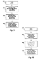
- Clock cycle 350 in Fig. 9 includes an act that begins a transfer of data from SRAM 240 to holding register 330 by fetching a first microinstruction ( ⁇ lnst1).
- ⁇ lnst1 includes an address processor instruction that includes an address processor opcode and an address processor register specifier. The instruction, when executed by address processor 170, produces an address in SRAM 240 that is loaded into CMAR 172.
- Clock cycle 354 includes an act that executes ⁇ lnst2, providing signals that read enable each processing unit's SRAM 240 so that data units are read from the addressed location and transferred through buses 242 and 244. This act also provides signals that load the data units into each processing unit's registered transceiver 212, referred to in Figs. 9-13 as "PU Registers.” Clock cycle 354 also includes an act that fetches a third microinstruction (ulnst3) whose address was loaded into MAR 152 during clock cycle 352.
- Clock cycle 412 includes an act that executes ⁇ lnst1, providing the address processor instruction to address processor 170 and providing signals so that the address produced by address processor 170 is loaded into CMAR 172. Address processor 170 also executes the address processor instruction during clock cycle 412. The act that executes ⁇ lnst1 also provides signals so that holding register 330 drives common bus 194 and registered transceivers 312 through 314 load data. Clock cycle 412 also includes an act that fetches a second microinstruction ( ⁇ lnst2) whose address was loaded into MAR 152 during clock cycle 410. ⁇ lnst2 specifies registered transceiver 212 as a source for buses 242 and 244 in each processing unit and also specifies in which processing units SRAM 240 should be written.
- ⁇ lnst2 specifies registered transceiver 212 as a source for buses 242 and 244 in each processing unit and also specifies in which processing units SRAM 240 should be written.
- ⁇ lnst1 only includes a 16 bit constant
- two iterations could be performed to provide one 16 bit constant on bus 242 and another on bus 244; in some cases, the same 16 bit constant could be provided in a single iteration on both buses 242 and 244, such as by copying the constant into both the upper and lower parts of constant buffers 192.
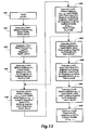
- Fig. 13 illustrates a pipelined transfer of data using holding register 330.
- Clock cycle 430 in Fig. 13 includes an act that begins a pipelined transfer of data from between SRAMs by fetching a first microinstruction ( ⁇ lnst1).
- ⁇ lnst1 includes an address processor instruction that includes an address processor opcode and an address processor register specifier. The instruction, when executed by address processor 170, produces an address m 0 that is loaded into CMAR 172.
- Clock cycle 434 includes an act that executes ⁇ lnst2, providing signals that read enable each processing unit's SRAM 240 so that data units are read from the location at address m 0 and transferred through buses 242 and 244. This act also provides signals that load the data units into each processing unit's registered transceiver 212.
- Clock cycle 434 also includes an act that fetches a third microinstruction ( ⁇ lnst3) whose address was loaded into MAR 152 during clock cycle 432.
- the invention could be applied in many ways, including image processing of the type described in U.S. Patent Nos. US-A 5,065,437; 5,048,109; 5,129,014; and 5,131,049.
- image processing techniques use data defining a first image to obtain a second image through operations such as erosion and dilation, operations that are defined in the Serra books cited above.
- Such operations can, for example, be performed by a series of suboperations each of which shifts an original image to obtain a shifted image and then performs a Boolean operation with values from the original image and the shifted image at each location.
- Some parts of the shifting operation can be performed with data transfers implemented as described above.
- RISC reduced instruction set
Applications Claiming Priority (2)
| Application Number | Priority Date | Filing Date | Title |
|---|---|---|---|
| US07/993,218 US5450603A (en) | 1992-12-18 | 1992-12-18 | SIMD architecture with transfer register or value source circuitry connected to bus |
| US993218 | 1992-12-18 |
Publications (3)
| Publication Number | Publication Date |
|---|---|
| EP0602909A2 true EP0602909A2 (de) | 1994-06-22 |
| EP0602909A3 EP0602909A3 (de) | 1994-07-06 |
| EP0602909B1 EP0602909B1 (de) | 1999-11-10 |
Family
ID=25539256
Family Applications (1)
| Application Number | Title | Priority Date | Filing Date |
|---|---|---|---|
| EP93309971A Expired - Lifetime EP0602909B1 (de) | 1992-12-18 | 1993-12-10 | SIMD-Architektur mit einem Bus zur Datenübertragung von und zu Verarbeitungseinheiten |
Country Status (4)
| Country | Link |
|---|---|
| US (1) | US5450603A (de) |
| EP (1) | EP0602909B1 (de) |
| JP (1) | JPH06223209A (de) |
| DE (1) | DE69326986T2 (de) |
Cited By (5)
| Publication number | Priority date | Publication date | Assignee | Title |
|---|---|---|---|---|
| EP0726532A2 (de) * | 1995-02-10 | 1996-08-14 | International Business Machines Corporation | Arrayprozessorarchitektur zur Kommunikation mit Rundsendebefehlen |
| GB2352306A (en) * | 1999-04-09 | 2001-01-24 | Pixelfusion Ltd | Parallel processing apparatus using a SIMD array |
| US7506136B2 (en) | 1999-04-09 | 2009-03-17 | Clearspeed Technology Plc | Parallel data processing apparatus |
| US7526630B2 (en) | 1999-04-09 | 2009-04-28 | Clearspeed Technology, Plc | Parallel data processing apparatus |
| US7627736B2 (en) | 1999-04-09 | 2009-12-01 | Clearspeed Technology Plc | Thread manager to control an array of processing elements |
Families Citing this family (49)
| Publication number | Priority date | Publication date | Assignee | Title |
|---|---|---|---|---|
| US5354695A (en) * | 1992-04-08 | 1994-10-11 | Leedy Glenn J | Membrane dielectric isolation IC fabrication |
| US5651121A (en) * | 1992-12-18 | 1997-07-22 | Xerox Corporation | Using mask operand obtained from composite operand to perform logic operation in parallel with composite operand |
| US5655131A (en) * | 1992-12-18 | 1997-08-05 | Xerox Corporation | SIMD architecture for connection to host processor's bus |
| DE4344157A1 (de) * | 1993-12-23 | 1995-06-29 | Philips Patentverwaltung | Funkgerät |
| US5557734A (en) * | 1994-06-17 | 1996-09-17 | Applied Intelligent Systems, Inc. | Cache burst architecture for parallel processing, such as for image processing |
| US5754590A (en) * | 1996-05-17 | 1998-05-19 | Lucent Technologies, Inc. | Modem architecture for integrated controller and data pump applications |
| US6551857B2 (en) | 1997-04-04 | 2003-04-22 | Elm Technology Corporation | Three dimensional structure integrated circuits |
| JPH1115773A (ja) * | 1997-06-24 | 1999-01-22 | Matsushita Electron Corp | 半導体集積回路、コンピュータシステム、データ処理装置及びデータ処理方法 |
| WO1999048025A2 (en) | 1998-03-18 | 1999-09-23 | Koninklijke Philips Electronics N.V. | Data processing device and method of computing the cosine transform of a matrix |
| US6219733B1 (en) | 1998-08-26 | 2001-04-17 | International Business Machines Corporation | Transmission line loop |
| CA2383526A1 (en) | 1999-09-01 | 2001-03-15 | Intel Corporation | Branch instruction for multithreaded processor |
| US7546444B1 (en) | 1999-09-01 | 2009-06-09 | Intel Corporation | Register set used in multithreaded parallel processor architecture |
| JP3971535B2 (ja) * | 1999-09-10 | 2007-09-05 | 株式会社リコー | Simd型プロセッサ |
| US7681018B2 (en) | 2000-08-31 | 2010-03-16 | Intel Corporation | Method and apparatus for providing large register address space while maximizing cycletime performance for a multi-threaded register file set |
| US20020053017A1 (en) * | 2000-09-01 | 2002-05-02 | Adiletta Matthew J. | Register instructions for a multithreaded processor |
| US7225281B2 (en) * | 2001-08-27 | 2007-05-29 | Intel Corporation | Multiprocessor infrastructure for providing flexible bandwidth allocation via multiple instantiations of separate data buses, control buses and support mechanisms |
| US6868476B2 (en) | 2001-08-27 | 2005-03-15 | Intel Corporation | Software controlled content addressable memory in a general purpose execution datapath |
| US7487505B2 (en) | 2001-08-27 | 2009-02-03 | Intel Corporation | Multithreaded microprocessor with register allocation based on number of active threads |
| US7216204B2 (en) | 2001-08-27 | 2007-05-08 | Intel Corporation | Mechanism for providing early coherency detection to enable high performance memory updates in a latency sensitive multithreaded environment |
| US7177988B2 (en) * | 2002-01-24 | 2007-02-13 | Broadcom Corporation | Method and system for synchronizing processor and DMA using ownership flags |
| US7610451B2 (en) | 2002-01-25 | 2009-10-27 | Intel Corporation | Data transfer mechanism using unidirectional pull bus and push bus |
| US6806737B2 (en) * | 2002-03-21 | 2004-10-19 | Raymond Jit-Hung Sung | Bi-directional amplifier and method for accelerated bus line communication |
| US6803782B2 (en) * | 2002-03-21 | 2004-10-12 | John Conrad Koob | Arrayed processing element redundancy architecture |
| US7437724B2 (en) * | 2002-04-03 | 2008-10-14 | Intel Corporation | Registers for data transfers |
| US7402897B2 (en) | 2002-08-08 | 2008-07-22 | Elm Technology Corporation | Vertical system integration |
| US7337275B2 (en) * | 2002-08-13 | 2008-02-26 | Intel Corporation | Free list and ring data structure management |
| US7116840B2 (en) | 2002-10-31 | 2006-10-03 | Microsoft Corporation | Decoding and error correction in 2-D arrays |
| US7133563B2 (en) | 2002-10-31 | 2006-11-07 | Microsoft Corporation | Passive embedded interaction code |
| US6941438B2 (en) | 2003-01-10 | 2005-09-06 | Intel Corporation | Memory interleaving |
| US7583842B2 (en) | 2004-01-06 | 2009-09-01 | Microsoft Corporation | Enhanced approach of m-array decoding and error correction |
| US7263224B2 (en) | 2004-01-16 | 2007-08-28 | Microsoft Corporation | Strokes localization by m-array decoding and fast image matching |
| US7607076B2 (en) | 2005-02-18 | 2009-10-20 | Microsoft Corporation | Embedded interaction code document |
| US7826074B1 (en) | 2005-02-25 | 2010-11-02 | Microsoft Corporation | Fast embedded interaction code printing with custom postscript commands |
| US7542976B2 (en) * | 2005-04-22 | 2009-06-02 | Microsoft Corporation | Local metadata embedding and decoding |
| US7599560B2 (en) | 2005-04-22 | 2009-10-06 | Microsoft Corporation | Embedded interaction code recognition |
| US7421439B2 (en) | 2005-04-22 | 2008-09-02 | Microsoft Corporation | Global metadata embedding and decoding |
| US7400777B2 (en) | 2005-05-25 | 2008-07-15 | Microsoft Corporation | Preprocessing for information pattern analysis |
| US7729539B2 (en) | 2005-05-31 | 2010-06-01 | Microsoft Corporation | Fast error-correcting of embedded interaction codes |
| US7580576B2 (en) | 2005-06-02 | 2009-08-25 | Microsoft Corporation | Stroke localization and binding to electronic document |
| US7619607B2 (en) | 2005-06-30 | 2009-11-17 | Microsoft Corporation | Embedding a pattern design onto a liquid crystal display |
| US7622182B2 (en) | 2005-08-17 | 2009-11-24 | Microsoft Corporation | Embedded interaction code enabled display |
| US7817816B2 (en) | 2005-08-17 | 2010-10-19 | Microsoft Corporation | Embedded interaction code enabled surface type identification |
| JP4720436B2 (ja) * | 2005-11-01 | 2011-07-13 | 株式会社日立製作所 | リコンフィギュラブルプロセッサまたは装置 |
| US7584342B1 (en) * | 2005-12-15 | 2009-09-01 | Nvidia Corporation | Parallel data processing systems and methods using cooperative thread arrays and SIMD instruction issue |
| US7788468B1 (en) | 2005-12-15 | 2010-08-31 | Nvidia Corporation | Synchronization of threads in a cooperative thread array |
| US7861060B1 (en) * | 2005-12-15 | 2010-12-28 | Nvidia Corporation | Parallel data processing systems and methods using cooperative thread arrays and thread identifier values to determine processing behavior |
| CN102508643A (zh) * | 2011-11-16 | 2012-06-20 | 刘大可 | 一种多核并行数字信号处理器及并行指令集的运行方法 |
| US9262704B1 (en) * | 2015-03-04 | 2016-02-16 | Xerox Corporation | Rendering images to lower bits per pixel formats using reduced numbers of registers |
| JP6627630B2 (ja) * | 2016-04-15 | 2020-01-08 | 富士通株式会社 | コンパイル方法、コンパイルプログラム及び情報処理装置 |
Citations (3)
| Publication number | Priority date | Publication date | Assignee | Title |
|---|---|---|---|---|
| EP0147851A2 (de) * | 1983-12-29 | 1985-07-10 | CHINOIN Gyogyszer és Vegyészeti Termékek Gyára RT. | Wasserlösliche Formen von Polyenantibiotika und Verfahren zu ihrer Herstellung |
| EP0236762A1 (de) * | 1986-03-08 | 1987-09-16 | Hitachi, Ltd. | Multiprozessorsystem |
| JPS63276659A (ja) * | 1987-03-27 | 1988-11-14 | Nec Corp | 複合コンピユ−タシステム |
Family Cites Families (18)
| Publication number | Priority date | Publication date | Assignee | Title |
|---|---|---|---|---|
| US4204251A (en) * | 1977-12-28 | 1980-05-20 | Finn Brudevold | Interconnection unit for multiple data processing systems |
| JPS56164464A (en) * | 1980-05-21 | 1981-12-17 | Tatsuo Nogi | Parallel processing computer |
| US4745546A (en) * | 1982-06-25 | 1988-05-17 | Hughes Aircraft Company | Column shorted and full array shorted functional plane for use in a modular array processor and method for using same |
| JPS60501286A (ja) * | 1983-05-12 | 1985-08-08 | アメリカン テレフオン アンド テレグラフ カムパニ− | 通信ネットワ−ク |
| US4814973A (en) * | 1983-05-31 | 1989-03-21 | Hillis W Daniel | Parallel processor |
| JPH0642237B2 (ja) * | 1983-12-28 | 1994-06-01 | 株式会社日立製作所 | 並列処理装置 |
| US4850027A (en) * | 1985-07-26 | 1989-07-18 | International Business Machines Corporation | Configurable parallel pipeline image processing system |
| US4831519A (en) * | 1985-12-12 | 1989-05-16 | Itt Corporation | Cellular array processor with variable nesting depth vector control by selective enabling of left and right neighboring processor cells |
| US4984235A (en) * | 1987-04-27 | 1991-01-08 | Thinking Machines Corporation | Method and apparatus for routing message packets and recording the roofing sequence |
| US5129092A (en) * | 1987-06-01 | 1992-07-07 | Applied Intelligent Systems,Inc. | Linear chain of parallel processors and method of using same |
| EP0293701B1 (de) * | 1987-06-01 | 1994-08-10 | Applied Intelligent Systems, Inc. | Paralleles Nachbarverarbeitungssystem und -Verfahren |
| US5297255A (en) * | 1987-07-28 | 1994-03-22 | Hitachi, Ltd. | Parallel computer comprised of processor elements having a local memory and an enhanced data transfer mechanism |
| US5113510A (en) * | 1987-12-22 | 1992-05-12 | Thinking Machines Corporation | Method and apparatus for operating a cache memory in a multi-processor |
| US5148547A (en) * | 1988-04-08 | 1992-09-15 | Thinking Machines Corporation | Method and apparatus for interfacing bit-serial parallel processors to a coprocessor |
| US5268856A (en) * | 1988-06-06 | 1993-12-07 | Applied Intelligent Systems, Inc. | Bit serial floating point parallel processing system and method |
| US5280547A (en) * | 1990-06-08 | 1994-01-18 | Xerox Corporation | Dense aggregative hierarhical techniques for data analysis |
| US5325500A (en) * | 1990-12-14 | 1994-06-28 | Xerox Corporation | Parallel processing units on a substrate, each including a column of memory |
| US5148500A (en) * | 1991-01-24 | 1992-09-15 | Aoi Systems, Inc. | Morphological processing system |
-
1992
- 1992-12-18 US US07/993,218 patent/US5450603A/en not_active Expired - Fee Related
-
1993
- 1993-12-10 DE DE69326986T patent/DE69326986T2/de not_active Expired - Fee Related
- 1993-12-10 EP EP93309971A patent/EP0602909B1/de not_active Expired - Lifetime
- 1993-12-14 JP JP5313843A patent/JPH06223209A/ja active Pending
Patent Citations (3)
| Publication number | Priority date | Publication date | Assignee | Title |
|---|---|---|---|---|
| EP0147851A2 (de) * | 1983-12-29 | 1985-07-10 | CHINOIN Gyogyszer és Vegyészeti Termékek Gyára RT. | Wasserlösliche Formen von Polyenantibiotika und Verfahren zu ihrer Herstellung |
| EP0236762A1 (de) * | 1986-03-08 | 1987-09-16 | Hitachi, Ltd. | Multiprozessorsystem |
| JPS63276659A (ja) * | 1987-03-27 | 1988-11-14 | Nec Corp | 複合コンピユ−タシステム |
Non-Patent Citations (1)
| Title |
|---|
| PATENT ABSTRACTS OF JAPAN vol. 13, no. 96 (P-839)(3444) 7 March 1989 & JP-A-63 276 659 (N.E.C. CORP) 14 November 1988 * |
Cited By (7)
| Publication number | Priority date | Publication date | Assignee | Title |
|---|---|---|---|---|
| EP0726532A2 (de) * | 1995-02-10 | 1996-08-14 | International Business Machines Corporation | Arrayprozessorarchitektur zur Kommunikation mit Rundsendebefehlen |
| EP0726532A3 (de) * | 1995-02-10 | 1997-03-19 | Ibm | Arrayprozessorarchitektur zur Kommunikation mit Rundsendebefehlen |
| US5659785A (en) * | 1995-02-10 | 1997-08-19 | International Business Machines Corporation | Array processor communication architecture with broadcast processor instructions |
| GB2352306A (en) * | 1999-04-09 | 2001-01-24 | Pixelfusion Ltd | Parallel processing apparatus using a SIMD array |
| US7506136B2 (en) | 1999-04-09 | 2009-03-17 | Clearspeed Technology Plc | Parallel data processing apparatus |
| US7526630B2 (en) | 1999-04-09 | 2009-04-28 | Clearspeed Technology, Plc | Parallel data processing apparatus |
| US7627736B2 (en) | 1999-04-09 | 2009-12-01 | Clearspeed Technology Plc | Thread manager to control an array of processing elements |
Also Published As
| Publication number | Publication date |
|---|---|
| US5450603A (en) | 1995-09-12 |
| JPH06223209A (ja) | 1994-08-12 |
| EP0602909A3 (de) | 1994-07-06 |
| DE69326986T2 (de) | 2000-04-27 |
| EP0602909B1 (de) | 1999-11-10 |
| DE69326986D1 (de) | 1999-12-16 |
Similar Documents
| Publication | Publication Date | Title |
|---|---|---|
| EP0602909B1 (de) | SIMD-Architektur mit einem Bus zur Datenübertragung von und zu Verarbeitungseinheiten | |
| US5437045A (en) | Parallel processing with subsampling/spreading circuitry and data transfer circuitry to and from any processing unit | |
| EP0602915B1 (de) | Einzelbefehl- und Mehrfachdatenarchitektur (SIMD) zur Verbindung mit dem Bus eines Hauptprozessors | |
| US4873626A (en) | Parallel processing system with processor array having memory system included in system memory | |
| US5165023A (en) | Parallel processing system with processor array and network communications system for transmitting messages of variable length | |
| US4891787A (en) | Parallel processing system with processor array having SIMD/MIMD instruction processing | |
| US6260088B1 (en) | Single integrated circuit embodying a risc processor and a digital signal processor | |
| US5559951A (en) | Page printer controller including a single chip superscalar microprocessor with graphics functional units | |
| US5872987A (en) | Massively parallel computer including auxiliary vector processor | |
| US5606520A (en) | Address generator with controllable modulo power of two addressing capability | |
| US5968167A (en) | Multi-threaded data processing management system | |
| US6038584A (en) | Synchronized MIMD multi-processing system and method of operation | |
| US5961628A (en) | Load and store unit for a vector processor | |
| US5418970A (en) | Parallel processing system with processor array with processing elements addressing associated memories using host supplied address value and base register content | |
| US4509116A (en) | Special instruction processing unit for data processing system | |
| US6948050B1 (en) | Single integrated circuit embodying a dual heterogenous processors with separate instruction handling hardware | |
| JPH06149545A (ja) | Cpuと乗算器とを有する半導体集積回路 | |
| US5450604A (en) | Data rotation using parallel to serial units that receive data from memory units and rotation buffer that provides rotated data to memory units | |
| WO2001084297A2 (en) | Flexible and efficient processor for use in image processing | |
| EP0036185A2 (de) | Datenverarbeitungssystem mit einer arithmetischen Ein-Chip-Kontrolleinheit unter Anwendung einer hochintegrierten Halbleitervorrichtung | |
| KR20010031192A (ko) | 기계시각시스템에서의 영상데이터와 같은 논리적으로인접한 데이터샘플들을 위한 데이터처리시스템 | |
| US5428804A (en) | Edge crossing circuitry for SIMD architecture | |
| KR940011594B1 (ko) | 공유 제어 기억부를 가진 멀티프로세서 제어기 및 그 동기화 방법 | |
| US6728741B2 (en) | Hardware assist for data block diagonal mirror image transformation | |
| JP2680828B2 (ja) | ディジタル装置 |
Legal Events
| Date | Code | Title | Description |
|---|---|---|---|
| PUAI | Public reference made under article 153(3) epc to a published international application that has entered the european phase |
Free format text: ORIGINAL CODE: 0009012 |
|
| PUAL | Search report despatched |
Free format text: ORIGINAL CODE: 0009013 |
|
| AK | Designated contracting states |
Kind code of ref document: A2 Designated state(s): DE FR GB |
|
| AK | Designated contracting states |
Kind code of ref document: A3 Designated state(s): DE FR GB |
|
| 17P | Request for examination filed |
Effective date: 19950109 |
|
| 17Q | First examination report despatched |
Effective date: 19970611 |
|
| GRAG | Despatch of communication of intention to grant |
Free format text: ORIGINAL CODE: EPIDOS AGRA |
|
| GRAG | Despatch of communication of intention to grant |
Free format text: ORIGINAL CODE: EPIDOS AGRA |
|
| GRAH | Despatch of communication of intention to grant a patent |
Free format text: ORIGINAL CODE: EPIDOS IGRA |
|
| GRAH | Despatch of communication of intention to grant a patent |
Free format text: ORIGINAL CODE: EPIDOS IGRA |
|
| GRAA | (expected) grant |
Free format text: ORIGINAL CODE: 0009210 |
|
| AK | Designated contracting states |
Kind code of ref document: B1 Designated state(s): DE FR GB |
|
| REF | Corresponds to: |
Ref document number: 69326986 Country of ref document: DE Date of ref document: 19991216 |
|
| ET | Fr: translation filed | ||
| PLBE | No opposition filed within time limit |
Free format text: ORIGINAL CODE: 0009261 |
|
| STAA | Information on the status of an ep patent application or granted ep patent |
Free format text: STATUS: NO OPPOSITION FILED WITHIN TIME LIMIT |
|
| 26N | No opposition filed | ||
| REG | Reference to a national code |
Ref country code: GB Ref legal event code: IF02 |
|
| PGFP | Annual fee paid to national office [announced via postgrant information from national office to epo] |
Ref country code: DE Payment date: 20041202 Year of fee payment: 12 |
|
| PGFP | Annual fee paid to national office [announced via postgrant information from national office to epo] |
Ref country code: GB Payment date: 20041208 Year of fee payment: 12 |
|
| PGFP | Annual fee paid to national office [announced via postgrant information from national office to epo] |
Ref country code: FR Payment date: 20050825 Year of fee payment: 13 |
|
| PG25 | Lapsed in a contracting state [announced via postgrant information from national office to epo] |
Ref country code: GB Free format text: LAPSE BECAUSE OF NON-PAYMENT OF DUE FEES Effective date: 20051210 |
|
| PG25 | Lapsed in a contracting state [announced via postgrant information from national office to epo] |
Ref country code: DE Free format text: LAPSE BECAUSE OF NON-PAYMENT OF DUE FEES Effective date: 20060701 |
|
| GBPC | Gb: european patent ceased through non-payment of renewal fee |
Effective date: 20051210 |
|
| REG | Reference to a national code |
Ref country code: FR Ref legal event code: ST Effective date: 20070831 |
|
| PG25 | Lapsed in a contracting state [announced via postgrant information from national office to epo] |
Ref country code: FR Free format text: LAPSE BECAUSE OF NON-PAYMENT OF DUE FEES Effective date: 20070102 |