EP0602772A1 - Mehrprozessorsystem - Google Patents
Mehrprozessorsystem Download PDFInfo
- Publication number
- EP0602772A1 EP0602772A1 EP93306726A EP93306726A EP0602772A1 EP 0602772 A1 EP0602772 A1 EP 0602772A1 EP 93306726 A EP93306726 A EP 93306726A EP 93306726 A EP93306726 A EP 93306726A EP 0602772 A1 EP0602772 A1 EP 0602772A1
- Authority
- EP
- European Patent Office
- Prior art keywords
- address
- data
- processor
- space
- address translation
- Prior art date
- Legal status (The legal status is an assumption and is not a legal conclusion. Google has not performed a legal analysis and makes no representation as to the accuracy of the status listed.)
- Granted
Links
Images


Classifications
-
- G—PHYSICS
- G06—COMPUTING; CALCULATING OR COUNTING
- G06F—ELECTRIC DIGITAL DATA PROCESSING
- G06F12/00—Accessing, addressing or allocating within memory systems or architectures
- G06F12/02—Addressing or allocation; Relocation
- G06F12/08—Addressing or allocation; Relocation in hierarchically structured memory systems, e.g. virtual memory systems
- G06F12/10—Address translation
- G06F12/1072—Decentralised address translation, e.g. in distributed shared memory systems
-
- G—PHYSICS
- G06—COMPUTING; CALCULATING OR COUNTING
- G06F—ELECTRIC DIGITAL DATA PROCESSING
- G06F12/00—Accessing, addressing or allocating within memory systems or architectures
- G06F12/02—Addressing or allocation; Relocation
- G06F12/0223—User address space allocation, e.g. contiguous or non contiguous base addressing
- G06F12/0284—Multiple user address space allocation, e.g. using different base addresses
-
- G—PHYSICS
- G06—COMPUTING; CALCULATING OR COUNTING
- G06F—ELECTRIC DIGITAL DATA PROCESSING
- G06F12/00—Accessing, addressing or allocating within memory systems or architectures
- G06F12/02—Addressing or allocation; Relocation
- G06F12/06—Addressing a physical block of locations, e.g. base addressing, module addressing, memory dedication
- G06F12/0646—Configuration or reconfiguration
- G06F12/0692—Multiconfiguration, e.g. local and global addressing
-
- G—PHYSICS
- G06—COMPUTING; CALCULATING OR COUNTING
- G06F—ELECTRIC DIGITAL DATA PROCESSING
- G06F15/00—Digital computers in general; Data processing equipment in general
- G06F15/16—Combinations of two or more digital computers each having at least an arithmetic unit, a program unit and a register, e.g. for a simultaneous processing of several programs
- G06F15/163—Interprocessor communication
- G06F15/17—Interprocessor communication using an input/output type connection, e.g. channel, I/O port
Definitions
- the present invention relates to multiprocessor systems in which processors communicate with each other to execute parallel processing and, more particularly, to methods and apparatus for transferring and processing data in such multiprocessor systems.
- a multiprocessor system As one multiprocessing technique using plural processors, a multiprocessor system has been proposed in which main storage is distributed among plural portions, controlled by their respective processors, which execute parallel processing.
- This multiprocessor system may be referred to as a memory-distributed parallel processing system, for example.
- processors operate in parallel while exchanging data with each other via a communication system. Thus, all the processors operate concurrently to execute one process.
- a calculation when a calculation is performed by such a multiprocessor system, data that is necessary for a first processor to execute the calculation is conveyed from those storage regions of the main storage which are ancillary to one or more second processors to the storage region of the main storage ancillary to the first processor.
- the first processor executes the calculation.
- the result of the calculation is stored in the storage region of the main storage ancillary to a third processor which is to hold or store the result. In this case, it is not necessary that the first through third processors all be separate units.
- some of the processors are a common processor.
- the processor system carries out parallel batch processing according to a sequence of procedures described above. The processors repeatedly execute the above-described processing synchronously, whereby parallel processing is performed.
- data is usually transferred between a first processor i for performing the arithmetic operations and a second processor j having data necessary for the arithmetic operations.
- the first processor i transmits to the second processor j a request for the transfer.
- the second processor j transfers data about reading to the first processor i .
- the second processor j causes data to be written to the storage region of the main storage ancillary to the first processor i .
- a system for transferring and processing data comprising a plurality of processors and a communication system for linking these processors together.
- the processors have storages for storing data and executing processing.
- the communication system transfers data and information between plural processors.
- the processors carry out processes in parallel, and each processor is constructed as described below.
- a common address translator section corresponds to a common space used by every processor, and translates a virtual address into a real address.
- An inherent address translator section corresponds to an inherent space used only by one processor incorporating this inherent address translator and translates a virtual address into a real address.
- a virtual address and a corresponding virtual address in the inherent address translator section are made to correspond to an identical real address.
- a transfer control section writes or reads data to or from a storage according to the real address translated by the inherent address translator section or by the common address translator section. Thus, data is transferred between the one processor and another processor.
- An arithmetic section reads data from the storage of the one processor according to a real address translated by the inherent address translator section of the one processor, provided that data transferred by the transfer control section exists in the common space corresponding to the common address translator section of the one processor. Then, the arithmetic section performs arithmetic operations.
- a method of transferring and processing data embodying the invention consists of transferring data and information between plural processors to cause them to execute parallel processing.
- a virtual address is translated into a real address by a common address translation corresponding to a common space used by every processor and by an inherent address translation corresponding to an inherent space used only by a corresponding one of the processors.
- the virtual address subjected to the common address translation and the virtual address subjected to the inherent address translation are made to correspond to an identical address.
- a step for controlling transfer data is written into or read from a storage of the one processor according to the real address translated by the inherent address translation or by the common address translation. Thus, data is transferred between the one processor and another processor.
- a step for performing calculations if data transferred to the one processor exists in the common space corresponding to the common address translation performed in the one processor, data is read from the storage of the one processor according to a real address translated by an intrinsic address translation performed in the one processor, and calculations are performed.
- an address control section is provided so that a virtual address applied to the common address translator section and a corresponding virtual address applied to the intrinsic address translator section are made to correspond to an identical real address.
- the transfer control section introduces the data necessary for the calculations into the common space from the other processor and then transfers the data to an intrinsic space.
- An information storage and a selector section may also be provided.
- the information storage stores access information indicating attributes for having access to the storage in the one processor and to the storage in the other processor, in association with data.
- the information storage section also stores space discrimination information for discriminating between the common space and the inherent space.
- the selector section selects either the inherent address translator section or the common address translator section according to the space discrimination information stored in the information storage.
- the aforementioned access information contains data about a processor that is to receive, data used to determine whether data is transferred for reading or writing, the length of the body of data, a transmitting address, and a receiving address.
- virtual addresses are translated into real addresses by both a common address translation corresponding to the common space used by every processor in common and by an inherent address translation corresponding to an inherent space used only by a corresponding one of the processors.
- the virtual address subjected to the common address translation and the virtual address subjected to the inherent address translation are made to correspond to an identical real address.
- data is written to or read from a storage according to the real address translated either by the inherent address translation or by the common address translation.
- the data is transferred between the one processor and the other processor.
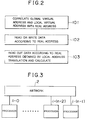
- FIG. 1 there is shown the structure of a first embodiment of a multiprocessor system containing a data transfer system embodying the invention.
- This multiprocessor system has a plurality of processors 1 which are linked together by a communication system 2.
- Each processor 1 has a storage 7 for storing data and executes given processing.
- the processors 1 transfer information such as data between each other via the communication system 2 and execute parallel processing.
- Each processor 1 has an inherent address translator section 4a, a common address translator section 4b, a transfer control section 6, and an arithmetic section 8, in addition to the storage 7 described above.
- the common address translator section 4b corresponds to a virtual global space that is a virtual address space used in common by all the processors 1.
- the translator section 4b translates a virtual address in the virtual global space into a real address in a real space.
- the inherent address translator section 4a corresponds to a virtual local space that is a virtual address space used only by a corresponding one of the processors 1, i.e., the processor 1 incorporating this translator section 4a, and translates a virtual address in the virtual local space into a real address in the real space.
- the virtual global space is principally a space used by all the processors 1 in common.
- the virtual local space is mainly used as a region in which local processes in one processor are performed.
- a virtual address in the global space which is applied to the common address translator section 4b and a corresponding virtual address in the local space which is applied to the inherent address translator section 4a are made to correspond to an identical real address.
- the transfer control section 6 writes or reads data to or from the storage 7 according to a real address translated by the inherent address translator section 4a or the common address translator section 4b. As a result, data is transferred between one processor 1 and another processor 1.
- the arithmetic section 8 If data transferred by the transfer control section 6 is present in the global space corresponding to the common address translator section 4b of the one processor, then the arithmetic section 8 reads data from the storage 7 of the one processor according to a real address in the local space corresponding to the inherent address translator section 4a of the one processor. Then, arithmetic operations are performed.
- a virtual address is translated into a real address by a global address translation corresponding to the global space used by all the processors 1 in common and by a local address translation corresponding to a local space used only by a corresponding one of the processors.
- a virtual address subjected to the global address translation and a virtual address subjected to the local address translation are made to correspond to an identical real address.
- transfer control step 102 data is written into or read from the storage according to a real address translated by the local address translation or by the global address translation. In this manner, data is transferred between the one processor 1 and another processor 1.
- arithmetic operation step 103 if the transferred data exists in the global space corresponding to the global address translation performed by the one processor 1, data is read from the storage of the one processor 1 according to a real address translated by the local address translation that is performed by the one processor 1. This processor 1 then performs arithmetic operations.
- the transfer control section 6 introduces the data necessary for the arithmetic operations into the global space from the another processor 1. The data is then transferred from the global space to the local space.
- a virtual address is translated into a real address by the global address translation corresponding to the global space used by every processor 1 in common and by the local address translation corresponding to the local space used only by a corresponding one of the processors 1.
- a virtual address subjected to the global address translation and a virtual address subjected to the local address translation are made to correspond to an identical address.
- the aforementioned one processor 1 writes or reads data to or from its storage 7 according to a real address produced by the local address translation or by the global address translation. Thus, data is transferred to or from another processor 1.
- Fig. 3 is a block diagram of a second embodiment of a multiprocessor system according to the present invention.
- Fig. 4 is a block diagram of each processor included in the system shown in Fig. 3, specifically showing the structure of the processor.
- the multiprocessor system is equipped with a plurality of processors 1-0 through 1-(n-1) for executing processing and with a network 2 for connecting together these processors to permit transfer of data therebetween.
- processors 1-0 through 1-(n-1) are hereinafter often described simply by processors 1.
- each processor 1 has a main storage 7, an instruction-processing section 8, and a transfer-processing section 10.
- a user program 72 consisting of a plurality of instructions and data are stored in the main storage 7.
- a transfer queue 3 is stored in the main storage 7. This queue 3 formed by registering a header, or the header of a data packet, containing access information indicating access attributes for gaining access to that main storage 7 which is controlled by the processor 1 transmitting data and for having access to that main storage 7 which is controlled by the processor 1 receiving the data.
- An operating system (OS) or a supervisory program 73 (hereinafter collectively referred to as the operating system) is also stored in the main storage 7 of each processor. This program assists the execution of the user program 72.
- the operating system 73 functions before the instructions of the user program are executed or dynamically functions at the request of the user program to load 32-bit address translation information into each entry of an address translation table 4 (described later).
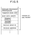
- Fig. 5 illustrates the structure of the transfer queue 3.
- a header for one packet is loaded into the transfer queue 3 at every transfer request.
- a header for one packet contains information for specifying a processor that is to receive, information about a transfer mode, information about the length of the body of data, an identifier (ID) for a transmitting space, a transmitting address, a receiving space ID, and a receiving address.
- ID identifier
- the information for specifying the receiving processor indicates the number given to a processor which should receive data.
- the information about the transfer mode indicates whether the data is read (R) or written (W).
- the information about the length of the body of data represents, in bytes, the data length of the body of the data in the form of packets specified by the header.
- the information about a transmitting address indicates the address of the data to be transmitted, the data being stored in the main storage 7 of the transmitting processor 1.
- the information about the receiving address indicates the address of data to be stored in the main storage 7 of the receiving processor.
- the transmitting space ID (identifier) is used to discriminate between a global transmitting space and a local transmitting space, as described in detail later.
- the receiving space ID is employed to discriminate between a global receiving space and a local receiving space.
- Each packet of data actually transmitted is composed of header and body data specified by the header.
- the instruction-processing section 8 of the processor 1 shown in Fig. 4 is coupled to the main storage 7, successively fetches instructions from the program in the main storage 7, and executes the instructions.
- the transfer-processing section 10 is coupled to the main storage 7 and to the instruction-processing section 8 to transfer the data in the form of the aforementioned packets between the main storage 7 of each processor 1 and the network 2.
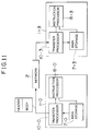
- Fig. 6 is a block diagram showing the structure of the transfer-processing section 10.
- the transfer-processing section 10 comprises a network transfer control section 11, a main storage access control section 6, an address translator section 13, a transfer queue base address register 14, a transfer queue reading pointer register 15, a transfer queue writing pointer register 16, and a data buffer 17.
- the transfer queue base address register 14 acts to hold the forefront address of the transfer queue 3 in the main storage 7.
- the transfer queue writing pointer register 16 serves to maintain a pointer indicating to which position (packet) within the transfer queue 3 the instruction-processing section 8 has placed, or enqueued, access information (transfer request).
- the transfer queue reading pointer register 15 holds a pointer indicating to which position (i.e., to which packet) within the transfer queue 3 the network transfer control section 11 has performed data transfer processing.
- the instruction-processing section 8 updates the values held in the transfer queue base address register 14, the transfer queue reading pointer register 15, and the transfer queue writing pointer register 16 or refers to these values.
- the network transfer control section 11 When activated by instructions from the instruction-processing section 8, the network transfer control section 11 waits for enqueuing of a request for transfer. The network transfer control section 11 starts data transfer processing in response to instructions for starting a transfer according to the reading pointer value from the transfer queue reading pointer register 15 and to the writing pointer value from the transfer queue writing pointer register 16. Then, the network transfer control section 11 produces a main storage access request to the main storage access control section 6, for reading the header and the body data of the packet to be transferred. The packet data read from the main storage 7 is sent to the network 2 via the data buffer 17.
- the main storage access control section 6 gains access to the main storage 7 at a request for main storage access from the network transfer control section 11, and controls transfer of packets between the main storage 7 and the data buffer 17.
- the data buffer 17 temporarily stores data when data is transmitted between the main storage 7 and the network 2. Also, the buffer 17 temporarily stores data when writing or reading into or from the main storage 7 is performed as dictated by the network transfer control section 11 and by the main storage access control section 6.
- the address translator section 13 translates addresses according to space ID value used for access to the main storage 7 specified by the header, and generates an access address to the main storage 7.
- the address translator section 13 translates a virtual address (logical address) into a real address (physical address).
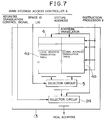
- Fig. 7 is a block diagram showing the structure of the address translator section 13.
- This translator section 13 has the aforementioned address translation table (memory) 4, a selector circuit 5, and another selector circuit 24.
- Each processor 1 assigns a global space and a local space to a virtual space used when data is transferred between processors 1.
- the address translation table 4 has a local address translation table 4a and a global address translation table 4b.
- Each processor 1 assigns a local space to a virtual space used when the instruction-processing section 8 of this processor performs arithmetic operations and control operations.
- the multiprocessor system executes programs in parallel while transferring data between processors, using the global space. Where data is calculated within each processor 1, it is necessary to transfer data from the global space to the local space. In an ordinary system, overhead increases because of transfer of data from the global space to the local space, thus hindering speedup of parallel processing.
- the local space in the instruction-processing section 8 and the local space in the transfer-processing section 10 are assigned to an identical real address.
- the local address translation table 4a and the global address translation table 4b are so created that a real address for the local space and a real address for the global space are assigned to an identical real address. This assignment is made by the operating system 73.
- the local address translation table 4a and the global address translation table 4b have plural entries corresponding to the number of bits of virtual addresses.
- the process in which a translation is made by the address translation table 4 is illustrated in Fig. 8.
- Fig. 8 In the example of Fig. 8, of 32 bits of virtual addresses, five bits from bit 04 to 08 are used for search in the translation table.
- the translation tables 4a and 4b have 32 entries from 00 to 31, corresponding to the aforementioned 5 bits of information.
- the address translation table 4 selects some entries from the local address translation table 4a and from the global address translation table 4b according to the value of the virtual address supplied from the main storage access control section 6.
- information about section address S of 4 bits, invalid bit I of 1 bit, access protection bit P of 1 bit, and 9 bits of information about a real address are stored in each entry of the translation tables 4a and 4b.
- the real address corresponds to the above 9 bits of an address translated from a virtual address.
- the 4 bits of the section address shown in Fig. 9 are used for comparison with the upper 4 bits of the virtual address supplied from the main storage access control section 6. If the virtual address and the section address agree, access to the main storage 7 is made. If they do not agree, "exception" is detected.
- invalid bit I is set to 1, meaning that neither writing nor reading of data is valid, and if access to a storage region corresponding to an entry is made, then the "exception" is detected. If invalid bit I is set to 0, writing and reading of data are performed.
- the access protection bit P is set to 0, and if reading access to a region corresponding to an entry is made, then data is read out. If the access protection bit P is set to 1, and if writing access is made, then the "exception" is detected.
- the selector circuit 5 receives the space ID specified by the header in the transfer queue 3 via the main storage access control section 6, and selects either one of the local address translation table 4a and the global address translation table 4b, depending on the space ID.
- the selector circuit 24 receives an address translation control signal and selects either the translated address from the selector circuit 5 or the virtual address from the main storage access control section 6, according to the address translation control signal.
- the address selected by the selector circuit 24 is used as a real address when access to the main storage 7 is made.
- Fig. 10 is a flowchart illustrating processing performed by the address translator section 13.
- Fig. 11 is a block diagram illustrating the functions of main sections of the translator section 13, for illustrating a writing access operation.
- Fig. 12 is a block diagram of main sections of the translator section 13, for illustrating a reading access operation.
- Fig. 11 when data is written to processor 1-3 from processor 1-0, for example, the following processing is performed.
- instruction-processing section 8-0 instructs transfer-processing section 10-0 to transfer data from main storage 7-0
- the transfer-processing section 10-0 first reads a header from the main storage 7-0. Then, the processing section reads body data and transfers them in the form of a packet to the network 2. Subsequently, transfer-processing section 10-3 writes the packet into main storage 7-3.
- the transfer-processing section 10-3 reads a packet consisting of header and body data from the main storage 7-3 according to the header of the request, whereby the section 10-3 makes a reading acknowledgement. Then, the transfer-processing section 10-0 writes the packet to the main storage 7-0.
- Fig. 13 is a flowchart illustrating processing for packet transmission. Operations for this processing are described next by referring to this figure.
- the operating system 73 loads information about address translation into every entry of the address translation table 4 before the instructions of the user program 72 are executed (step 201).
- the instruction-processing section 8 for executing the instructions of the user program 72 writes various kinds of information as access information for asking for data transfer to the transfer queue 3 in the main storage 7 as shown in Fig. 5, the information taking the form of the header of a packet.
- These various kinds of information include information for specifying a processor that is to receive, the length of body data, a transmitting address, a receiving address, the kind of transmitting space, and the kind of receiving space (step 202).
- the instruction-processing section 8 which executes the instructions of the user program 72 increments the value of the writing pointer in the transfer queue writing pointer section 16 (step 203).
- the instruction-processing section 8 which executes the instructions of the user program 72 repeatedly writes access information about the transfer request to the transfer queue 3 and increments the value of the writing pointer in the transfer queue writing pointer register 16. Then, the instruction-processing section 8 makes a decision as to whether writing to the transfer queue 3 (enqueuing) has ended (step 204).
- the network transfer control section 11 is activated by instructions from the instruction-processing section 8 and waits until the enqueuing of transfer request ends. If the instruction-processing section 8 ends the enqueuing, the network transfer control section 11 makes a decision as to whether the value of the transfer queuing reading pointer is coincident with the value of the transfer queuing writing pointer (step 205). If their values do not agree, the network transfer control section 11 judges that there is any unprocessed transfer request and starts transfer processing. The control section 11 causes a request for access to the main storage to the main storage access control section 6, for reading the header of the transfer packet.
- the main storage access control section 6 calculates the address in the main storage 7 for the packet header of the oldest unprocessed transfer request from the transfer queue base address and from the transfer queue reading pointer. The control section 6 then gives reading access to the transfer queue 3 in the main storage 7 via the address translator section 13.
- a main storage access control section 12 loads the packet header into the data buffer 17 and informs the network transfer control section 11 that the reading of the packet header has been completed (step 206).
- the main storage access control section 6 reads a transfer mode, a transmitting space ID, and a receiving space ID from the header held in the data buffer 17.
- An LL permission control section 30 incorporated in the network transfer control section 11 makes a decision as to whether transfer of data according to tables 31-33 should be permitted, by deferring to the transfer mode, the transmitting space ID, and the receiving space ID (step 207).
- the network transfer control section 11 extracts access information for transfer of a transmitting address, a receiving address, etc., calculates the address of the body data in the packet, and grants reading access to the main storage 7 via the address translator section 13 (step 208).
- the address translator section 13 performs processing as illustrated in Fig. 10. It accepts a virtual address from the main storage access control section 6 (step 401). Then, the translator section searches entries in the local address translation table 4a and in the global address translation table 4b according to the virtual address (step 402).
- the selector circuit 24 receives an address translation control signal indicating whether a virtual address should be translated into a real address, and selects either a translated address from the selector circuit 5 or a virtual address from the main storage access control section 6 according to the address translation control signal (step 403). This selected address becomes a real address when the main storage 7 is accessed.
- the address translation table 4 delivers real addresses, P, I, and S corresponding to entries in the translation tables 4a, 4b to the selector circuit 5 (step 405).
- the selector circuit 5 selects either the local address translation table 4a or the global address translation table 4b according to the space ID from the main storage access control section 6 (step 406).
- step 409 If the virtual address is coincident with the section address S, a decision is made as to whether the invalid bit is "1" or not (step 409). If the invalid bit is "1", exception of writing and reading of data is detected (step 408).
- step 410 If the invalid bit is 0, a decision is made as to whether the access protection bit P is bit "1" or not (step 410). If it is "1", exception of writing access is detected (step 408).
- the global space address table 4b is selected according to the space ID. In this case, the global space is common to all the processors. Therefore, when address translation information in the global address translation table 4b is rewritten, all the processors are synchronized.
- the local address translation address table 4a is selected according to the space ID. In this case, local spaces are inherent in their respective processors. Therefore, where address translation information in the local address translation table 4a is rewritten, it can be rewritten independent of other processors. If only rewriting of the local address translation table 4a is needed, then all the processors are not required to be synchronized. Consequently, the translation table can be rewritten with less overhead. The local address translation table 4a is rewritten more frequently than the global address translation table 4b.
- either the local address translation table 4a or the global address translation table 4b is selected.
- a virtual address is translated into a real address by the selected translation table.
- Body data in packets are successively read from the main storage 7. Then, the main storage access control section 6 loads the body data serially into the data buffer 17 and informs the network transfer control section 11 of the sequential amounts of body data read out (step 209).
- control section 11 If the network transfer control section 11 is informed of the end of the reading of headers of packets by the main storage access control section 6, the control section 11 extracts access information about a transfer request from the data buffer 17, inspects the information in a given manner, modifies the information, and writes the access information back into the data buffer 17.
- the network transfer control section 11 transmits packet headers to the network 2 from the data buffer 17 (step 210). If the control section 11 is informed of sequential amounts of body data in the form of packets read out by the main storage access control section 6, then the control section 11 sequentially transmits body data in the form of packets held in the data buffer 1 to the network 2 (step 211).
- the network transfer control section 11 increments the transfer queue reading pointer (step 212), and then control returns to step 205.
- the control section 11 compares the value of the transfer queue reading pointer with the value of the transfer queue writing pointer. If they do not agree, i.e. if any unprocessed transfer request remains, then the next transfer processing is performed (steps 206-212). The data transfer processing is repeated until the value in the transfer queue reading pointer is equal to the value in the transfer queue writing pointer. If they become coincident, the data transfer processing is ended (step 213).
- the processing described thus far is processing for transferring packets from a transmitting processor to a receiving processor. This processing is included in operations when writing access is made, as schematically shown in Fig. 11.
- FIG. 14 illustrates processing for writing to the receiving processor.
- the network 2 transfers packets from the transmitting processor and connects a processor that is to receive with the processor transmitting the packets according to the information specifying the receiving processor included in the header.
- the transfer-processing section 10 in the receiving processor receives packets from the network 2 (step 501).
- the data buffer 17 temporarily stores the packets (step 502).
- the main storage access control section 6 reads a header from the data buffer 17 (step 503), and gains access to the main storage 7 via the address translator section 13 according to the receiving address in the header (step 504).
- the local address translation table 4a and the global address translation table 4b translate virtual addresses into real addresses (step 505).
- the selector circuit 5 selects either the local address translation table 4a or the global address translation table 4b according to the receiving space ID in the header (step 506).
- FIG. 15 illustrates a part of the FORTRAN program created for serial processing. In this figure, one processor calculates arrays A and B in the FORTRAN program.
- a working array C is defined as well as the arrays A and B.
- the array B is assigned to the global spaces formed in the processors.
- the arrays A and C are assigned to the local spaces formed in the processors. Units of processing are assigned to the processors according to the value of I of a DO statement.
- Fig. 16 illustrates assignment of the arrays to 10 processors.
- partial array B (101:200) consisting of elements 101 to 200 which is a subset of array B is assigned to the global space in a processor 1-2 (PE2 in Fig. 16).
- the instruction-processing section 8 in the processor 1-2 performs calculations on an array of bits I from 101 to 200.
- An address translation table corresponding to a divided global space of array B is the global address translation table 4b provided in each processor.
- An address translation table corresponding to a divided local space of array C is the local address translation table 4a provided in each processor.
- a divided local space of array A is a virtual space in which the instruction-processing section 8 performs calculations.
- Fig. 17 illustrates a program to be executed by a processor.
- a program as shown in Fig. 17 is executed, if an address translation as in the described embodiment is not utilized, the following processing is performed.
- data Prior to calculations, data is transferred from global space B to local space C. With respect to B(100), data is read from the global space B of processor 1-1 and transferred to local space C. With respect to B(101:200), real addresses are different and so data is serially transferred from the global space of its processor 1-2 to the local space C. Then, B(201) is read from the global space of processor 1-3 and transferred to the local space C. In this way, processing is performed while changing the value of I from 100 to 201. After the completion of the processing, a calculation is performed on DO statement 10.
- Fig. 18 is a diagram illustrating mapping of arrays B and C in each processor onto a real main storage.
- Fig. 19 is a diagram illustrating a program that is a simplified version of the program to be processed.
- Fig. 20 is a flowchart illustrating an example of transfer processing.
- arrays C(100) through C(201) are assigned to the local space of processor 1-2.
- arrays B(100) through C(201) are assigned to the global space of the processor 1-2.
- Elements of the arrays in the local space and elements of the arrays in the global space are made to correspond to an identical address in a real memory space corresponding to a real address.
- array element C(200) and array element B(200) are both made to correspond to address 650. Every array element corresponds to 32 entries of each address translation table.
- the transfer-processing section 10 causes the main storage to transfer data from the global space to the local space (step 601).
- the array B(100) is read from the global space B in the processor 1-1 and transferred to the local space C (step 603).
- the global address translation table 4b and the local address translation table 4a are made to correspond to an identical real address. That is, it is not necessary to transfer data from the global space in the same processor 1-2 to the local space C.
- the array B(201) is read from the global space in processor 1-3 and transferred to the local space C (step 604).
- transfer processing is effected while changing I from 100 to 201 (step 605). Thereafter, a calculation is performed on DO statement 10 (step 606).
- the array C is a local space in the transfer-processing section 10 and, therefore, the array C is the same as the virtual space in the instruction-processing section 8. Consequently, the local space is used for calculations performed by the instruction-processing section 8.
Landscapes
- Engineering & Computer Science (AREA)
- Theoretical Computer Science (AREA)
- Physics & Mathematics (AREA)
- General Engineering & Computer Science (AREA)
- General Physics & Mathematics (AREA)
- Computer Hardware Design (AREA)
- Software Systems (AREA)
- Multi Processors (AREA)
- Memory System Of A Hierarchy Structure (AREA)
- Memory System (AREA)
Applications Claiming Priority (3)
| Application Number | Priority Date | Filing Date | Title |
|---|---|---|---|
| JP33850592 | 1992-12-18 | ||
| JP4338505A JP2974526B2 (ja) | 1992-12-18 | 1992-12-18 | データ転送処理方法及びデータ転送処理装置 |
| JP338505/92 | 1992-12-18 |
Publications (2)
| Publication Number | Publication Date |
|---|---|
| EP0602772A1 true EP0602772A1 (de) | 1994-06-22 |
| EP0602772B1 EP0602772B1 (de) | 2002-06-26 |
Family
ID=18318792
Family Applications (1)
| Application Number | Title | Priority Date | Filing Date |
|---|---|---|---|
| EP93306726A Expired - Lifetime EP0602772B1 (de) | 1992-12-18 | 1993-08-24 | Mehrprozessorsystem |
Country Status (4)
| Country | Link |
|---|---|
| US (1) | US5896501A (de) |
| EP (1) | EP0602772B1 (de) |
| JP (1) | JP2974526B2 (de) |
| DE (1) | DE69332058T2 (de) |
Cited By (2)
| Publication number | Priority date | Publication date | Assignee | Title |
|---|---|---|---|---|
| EP0817060A2 (de) * | 1996-07-02 | 1998-01-07 | Sun Microsystems, Inc. | Hierarchisches Datenverarbeitungssystem mit symetrischen Multiprozessoren |
| FR2771526A1 (fr) * | 1997-11-27 | 1999-05-28 | Bull Sa | Architecture pour la gestion de donnees vitales dans une machine multi-modulaire et procede pour la mise en oeuvre d'une telle architecture |
Families Citing this family (24)
| Publication number | Priority date | Publication date | Assignee | Title |
|---|---|---|---|---|
| JPH08297646A (ja) * | 1995-04-26 | 1996-11-12 | Kofu Nippon Denki Kk | 並列計算機 |
| JP3119214B2 (ja) * | 1997-09-30 | 2000-12-18 | ソニー株式会社 | 記憶装置、データ処理システム並びにデータの書き込み及び読み出し方法 |
| SE515461C2 (sv) * | 1998-10-05 | 2001-08-06 | Ericsson Telefon Ab L M | Metod och arrangemang för minneshantering |
| US6434618B1 (en) * | 1998-11-12 | 2002-08-13 | Lucent Technologies Inc. | Programmable network element for packet-switched computer network |
| US6574721B1 (en) * | 1999-08-31 | 2003-06-03 | International Business Machines Corporation | Apparatus and method for providing simultaneous local and global addressing using software to distinguish between local and global addresses |
| JP4688316B2 (ja) * | 2001-02-28 | 2011-05-25 | 独立行政法人産業技術総合研究所 | シミュレーション装置とシミュレーション方法、及び映像生成装置と映像生成方法 |
| GB2390702B (en) * | 2002-04-22 | 2006-04-12 | Micron Technology Inc | Providing a register file memory with local addressing in a SIMD parallel processor |
| US7404015B2 (en) * | 2002-08-24 | 2008-07-22 | Cisco Technology, Inc. | Methods and apparatus for processing packets including accessing one or more resources shared among processing engines |
| US7304999B2 (en) * | 2002-08-24 | 2007-12-04 | Cisco Technology Inc. | Methods and apparatus for processing packets including distributing packets across multiple packet processing engines and gathering the processed packets from the processing engines |
| JP3904498B2 (ja) * | 2002-09-17 | 2007-04-11 | 沖電気工業株式会社 | プロセッサ間通信システム |
| EP1611513B1 (de) * | 2003-04-04 | 2010-12-15 | Oracle America, Inc. | Mehrknoten system, bei dem die globale adresse, die durch ein verarbeitungsuntersystem erzeugt wird, globale-zu-lokale übersetzungsinformationen miteinschliesst |
| US7363462B2 (en) * | 2003-04-04 | 2008-04-22 | Sun Microsystems, Inc. | Performing virtual to global address translation in processing subsystem |
| US7765381B2 (en) * | 2003-04-04 | 2010-07-27 | Oracle America, Inc. | Multi-node system in which home memory subsystem stores global to local address translation information for replicating nodes |
| JP2005332145A (ja) * | 2004-05-19 | 2005-12-02 | Nec Electronics Corp | データ転送制御回路及びデータ転送方法 |
| US7711909B1 (en) * | 2004-12-09 | 2010-05-04 | Oracle America, Inc. | Read sharing using global conflict indication and semi-transparent reading in a transactional memory space |
| US7490215B2 (en) * | 2004-12-22 | 2009-02-10 | Intel Corporation | Media memory system and method for providing concurrent memory access to a plurality of processors through separate translation table information |
| US8667249B2 (en) | 2004-12-22 | 2014-03-04 | Intel Corporation | Systems and methods exchanging data between processors through concurrent shared memory |
| US7551617B2 (en) | 2005-02-08 | 2009-06-23 | Cisco Technology, Inc. | Multi-threaded packet processing architecture with global packet memory, packet recirculation, and coprocessor |
| US7561589B2 (en) * | 2005-02-23 | 2009-07-14 | Cisco Technology, Inc | Virtual address storage which may be of particular use in generating fragmented packets |
| US7606250B2 (en) | 2005-04-05 | 2009-10-20 | Cisco Technology, Inc. | Assigning resources to items such as processing contexts for processing packets |
| US7739426B1 (en) | 2005-10-31 | 2010-06-15 | Cisco Technology, Inc. | Descriptor transfer logic |
| WO2009140631A2 (en) * | 2008-05-15 | 2009-11-19 | Smooth-Stone, Inc. | Distributed computing system with universal address system and method |
| EP3171277B1 (de) * | 2014-08-12 | 2021-03-03 | Huawei Technologies Co. Ltd. | Verfahren zur verwaltung von dateien, verteiltes speichersystem und verwaltungsknoten |
| GB2565146A (en) * | 2017-08-04 | 2019-02-06 | Kaleao Ltd | Memory control for electronic data processing system |
Citations (5)
| Publication number | Priority date | Publication date | Assignee | Title |
|---|---|---|---|---|
| EP0208428A2 (de) * | 1985-06-28 | 1987-01-14 | Hewlett-Packard Company | Direkte Ein-- und Ausgabe in einer virtuellen Speicheranordnung |
| JPH02118839A (ja) * | 1988-10-28 | 1990-05-07 | Nec Corp | タスク間のメッセージ通信方式 |
| EP0387644A1 (de) * | 1989-03-15 | 1990-09-19 | BULL HN INFORMATION SYSTEMS ITALIA S.p.A. | Mehrprozessoranordnung mit Vervielfältigung von globalen Daten und mit zwei Stufen von Adressübersetzungseinheiten |
| EP0431467A1 (de) * | 1989-12-04 | 1991-06-12 | BULL HN INFORMATION SYSTEMS ITALIA S.p.A. | Multiprozessorsystem mit verteilten gemeinsamen Betriebsmitteln und mit Vervielfältigung von globalen Daten |
| EP0457345A2 (de) * | 1990-05-18 | 1991-11-21 | Nec Corporation | Informationsverarbeitungsgerät |
Family Cites Families (18)
| Publication number | Priority date | Publication date | Assignee | Title |
|---|---|---|---|---|
| US4149242A (en) * | 1977-05-06 | 1979-04-10 | Bell Telephone Laboratories, Incorporated | Data interface apparatus for multiple sequential processors |
| US4388685A (en) * | 1978-08-04 | 1983-06-14 | Digital Equipment Corporation | Central processor with apparatus for extended virtual addressing |
| US4455602A (en) * | 1981-05-22 | 1984-06-19 | Data General Corporation | Digital data processing system having an I/O means using unique address providing and access priority control techniques |
| US4455647A (en) * | 1982-06-14 | 1984-06-19 | Siemens Corporation | Apparatus for establishing multi-address connections |
| US4485438A (en) * | 1982-06-28 | 1984-11-27 | Myrmo Erik R | High transfer rate between multi-processor units |
| US4731734A (en) * | 1983-10-17 | 1988-03-15 | Data General Corporation | Digital computer system incorporating object-based addressing and access control and tables defining derivation of addresses of data from operands in instructions |
| US4881164A (en) * | 1983-12-30 | 1989-11-14 | International Business Machines Corporation | Multi-microprocessor for controlling shared memory |
| US4742447A (en) * | 1986-01-16 | 1988-05-03 | International Business Machines Corporation | Method to control I/O accesses in a multi-tasking virtual memory virtual machine type data processing system |
| JPS62206658A (ja) * | 1986-03-07 | 1987-09-11 | Hitachi Ltd | 記憶管理装置 |
| US4843542A (en) * | 1986-11-12 | 1989-06-27 | Xerox Corporation | Virtual memory cache for use in multi-processing systems |
| US5036459A (en) * | 1989-03-09 | 1991-07-30 | U.S. Philips Corporation | Multi-processor computer system with distributed memory and an interprocessor communication mechanism, and method for operating such mechanism |
| JP2833062B2 (ja) * | 1989-10-30 | 1998-12-09 | 株式会社日立製作所 | キャッシュメモリ制御方法とこのキャッシュメモリ制御方法を用いたプロセッサおよび情報処理装置 |
| US5123094A (en) * | 1990-01-26 | 1992-06-16 | Apple Computer, Inc. | Interprocessor communications includes second CPU designating memory locations assigned to first CPU and writing their addresses into registers |
| JPH0512126A (ja) * | 1991-07-05 | 1993-01-22 | Hitachi Ltd | 仮想計算機のアドレス変換装置及びアドレス変換方法 |
| US5430850A (en) * | 1991-07-22 | 1995-07-04 | Massachusetts Institute Of Technology | Data processing system with synchronization coprocessor for multiple threads |
| JPH0619785A (ja) * | 1992-03-27 | 1994-01-28 | Matsushita Electric Ind Co Ltd | 分散共有仮想メモリーとその構成方法 |
| JP2625385B2 (ja) * | 1994-06-30 | 1997-07-02 | 日本電気株式会社 | マルチプロセッサシステム |
| US5606666A (en) * | 1994-07-19 | 1997-02-25 | International Business Machines Corporation | Method and apparatus for distributing control messages between interconnected processing elements by mapping control messages of a shared memory addressable by the receiving processing element |
-
1992
- 1992-12-18 JP JP4338505A patent/JP2974526B2/ja not_active Expired - Fee Related
-
1993
- 1993-08-24 EP EP93306726A patent/EP0602772B1/de not_active Expired - Lifetime
- 1993-08-24 DE DE69332058T patent/DE69332058T2/de not_active Expired - Fee Related
-
1997
- 1997-02-04 US US08/795,689 patent/US5896501A/en not_active Expired - Fee Related
Patent Citations (5)
| Publication number | Priority date | Publication date | Assignee | Title |
|---|---|---|---|---|
| EP0208428A2 (de) * | 1985-06-28 | 1987-01-14 | Hewlett-Packard Company | Direkte Ein-- und Ausgabe in einer virtuellen Speicheranordnung |
| JPH02118839A (ja) * | 1988-10-28 | 1990-05-07 | Nec Corp | タスク間のメッセージ通信方式 |
| EP0387644A1 (de) * | 1989-03-15 | 1990-09-19 | BULL HN INFORMATION SYSTEMS ITALIA S.p.A. | Mehrprozessoranordnung mit Vervielfältigung von globalen Daten und mit zwei Stufen von Adressübersetzungseinheiten |
| EP0431467A1 (de) * | 1989-12-04 | 1991-06-12 | BULL HN INFORMATION SYSTEMS ITALIA S.p.A. | Multiprozessorsystem mit verteilten gemeinsamen Betriebsmitteln und mit Vervielfältigung von globalen Daten |
| EP0457345A2 (de) * | 1990-05-18 | 1991-11-21 | Nec Corporation | Informationsverarbeitungsgerät |
Non-Patent Citations (2)
| Title |
|---|
| A. KABEMOTO AND H. YOSHIDA: "The architecture of the Sure System 2000 communications processor", IEEE MICRO, vol. 11, no. 4, August 1991 (1991-08-01), NEW YORK US, pages 28 - 78, XP000258591, DOI: doi:10.1109/40.85724 * |
| PATENT ABSTRACTS OF JAPAN vol. 14, no. 341 (P - 1081) 24 July 1990 (1990-07-24) * |
Cited By (8)
| Publication number | Priority date | Publication date | Assignee | Title |
|---|---|---|---|---|
| EP0817060A2 (de) * | 1996-07-02 | 1998-01-07 | Sun Microsystems, Inc. | Hierarchisches Datenverarbeitungssystem mit symetrischen Multiprozessoren |
| EP0817060A3 (de) * | 1996-07-02 | 1999-02-24 | Sun Microsystems, Inc. | Hierarchisches Datenverarbeitungssystem mit symetrischen Multiprozessoren |
| US6226671B1 (en) | 1996-07-02 | 2001-05-01 | Sun Microsystems, Inc. | Shared memory system for symmetric multiprocessor systems |
| US6578071B2 (en) * | 1996-07-02 | 2003-06-10 | Sun Microsystems, Inc. | Repeater for use in a shared memory computing system |
| US6826660B2 (en) | 1996-07-02 | 2004-11-30 | Sun Microsystems, Inc. | Hierarchical SMP computer system |
| FR2771526A1 (fr) * | 1997-11-27 | 1999-05-28 | Bull Sa | Architecture pour la gestion de donnees vitales dans une machine multi-modulaire et procede pour la mise en oeuvre d'une telle architecture |
| EP0919914A1 (de) * | 1997-11-27 | 1999-06-02 | Bull S.A. | Architektur zur Verwaltung vitaler Daten in einem mehrfach modularen Gerät und Verfahren zum Betrieb einer solchen Architektur |
| US6434679B1 (en) | 1997-11-27 | 2002-08-13 | Bull, S.A. | Architecture for vital data management in a multi-module machine and process for implementing an architecture of this type |
Also Published As
| Publication number | Publication date |
|---|---|
| US5896501A (en) | 1999-04-20 |
| JPH06187298A (ja) | 1994-07-08 |
| DE69332058T2 (de) | 2002-10-17 |
| EP0602772B1 (de) | 2002-06-26 |
| DE69332058D1 (de) | 2002-08-01 |
| JP2974526B2 (ja) | 1999-11-10 |
Similar Documents
| Publication | Publication Date | Title |
|---|---|---|
| US5896501A (en) | Multiprocessor system and parallel processing method for processing data transferred between processors | |
| US4956771A (en) | Method for inter-processor data transfer | |
| US4539637A (en) | Method and apparatus for handling interprocessor calls in a multiprocessor system | |
| US5572680A (en) | Method and apparatus for processing and transferring data to processor and/or respective virtual processor corresponding to destination logical processor number | |
| US4675806A (en) | Data processing unit utilizing data flow ordered execution | |
| US5140682A (en) | Storage control apparatus | |
| US5450564A (en) | Method and apparatus for cache memory access with separate fetch and store queues | |
| US5129093A (en) | Method and apparatus for executing an operation request signal in a loosely coupled parallel computer having processor elements capable of updating memory contents and minimizing exclusive control of sharable distributed memories | |
| US5974533A (en) | Data processor | |
| US4750154A (en) | Memory alignment system and method | |
| US4683533A (en) | Storage control system using plural buffer address arrays | |
| US4881163A (en) | Computer system architecture employing cache data line move-out queue buffer | |
| US5418970A (en) | Parallel processing system with processor array with processing elements addressing associated memories using host supplied address value and base register content | |
| US5822785A (en) | Data transfer using local and global address translation and authorization | |
| EP2264617A1 (de) | Verfahren und Vorrichtung zur Replizierung einer Datenbank | |
| US3654621A (en) | Information processing system having means for dynamic memory address preparation | |
| US3680058A (en) | Information processing system having free field storage for nested processes | |
| EP0407087B1 (de) | Eingabewarteschlange für Speichersubsysteme | |
| EP0125044B1 (de) | Mikrocomputer mit Interprozesskommunikation | |
| US6732249B1 (en) | Host computer virtual memory within a network interface adapter | |
| JPH04257054A (ja) | チャネル間接続装置 | |
| US5297255A (en) | Parallel computer comprised of processor elements having a local memory and an enhanced data transfer mechanism | |
| US20020099922A1 (en) | Data processing apparatus including a plurality of pipeline processing mechanisms in which memory access instructions are carried out in a memory access pipeline | |
| AU597980B2 (en) | Apparatus and method for interprocessor communication | |
| US6128714A (en) | Method of processing a data move instruction for moving data between main storage and extended storage and data move instruction processing apparatus |
Legal Events
| Date | Code | Title | Description |
|---|---|---|---|
| PUAI | Public reference made under article 153(3) epc to a published international application that has entered the european phase |
Free format text: ORIGINAL CODE: 0009012 |
|
| AK | Designated contracting states |
Kind code of ref document: A1 Designated state(s): DE GB |
|
| 17P | Request for examination filed |
Effective date: 19940913 |
|
| 17Q | First examination report despatched |
Effective date: 20000809 |
|
| GRAG | Despatch of communication of intention to grant |
Free format text: ORIGINAL CODE: EPIDOS AGRA |
|
| GRAG | Despatch of communication of intention to grant |
Free format text: ORIGINAL CODE: EPIDOS AGRA |
|
| GRAH | Despatch of communication of intention to grant a patent |
Free format text: ORIGINAL CODE: EPIDOS IGRA |
|
| GRAH | Despatch of communication of intention to grant a patent |
Free format text: ORIGINAL CODE: EPIDOS IGRA |
|
| GRAA | (expected) grant |
Free format text: ORIGINAL CODE: 0009210 |
|
| AK | Designated contracting states |
Kind code of ref document: B1 Designated state(s): DE GB |
|
| REG | Reference to a national code |
Ref country code: GB Ref legal event code: FG4D |
|
| REF | Corresponds to: |
Ref document number: 69332058 Country of ref document: DE Date of ref document: 20020801 |
|
| PLBE | No opposition filed within time limit |
Free format text: ORIGINAL CODE: 0009261 |
|
| STAA | Information on the status of an ep patent application or granted ep patent |
Free format text: STATUS: NO OPPOSITION FILED WITHIN TIME LIMIT |
|
| 26N | No opposition filed |
Effective date: 20030327 |
|
| PGFP | Annual fee paid to national office [announced via postgrant information from national office to epo] |
Ref country code: DE Payment date: 20060817 Year of fee payment: 14 |
|
| PGFP | Annual fee paid to national office [announced via postgrant information from national office to epo] |
Ref country code: GB Payment date: 20060823 Year of fee payment: 14 |
|
| GBPC | Gb: european patent ceased through non-payment of renewal fee |
Effective date: 20070824 |
|
| PG25 | Lapsed in a contracting state [announced via postgrant information from national office to epo] |
Ref country code: DE Free format text: LAPSE BECAUSE OF NON-PAYMENT OF DUE FEES Effective date: 20080301 |
|
| PG25 | Lapsed in a contracting state [announced via postgrant information from national office to epo] |
Ref country code: GB Free format text: LAPSE BECAUSE OF NON-PAYMENT OF DUE FEES Effective date: 20070824 |