EP0602699A2 - Current limited power semiconductor device - Google Patents
Current limited power semiconductor device Download PDFInfo
- Publication number
- EP0602699A2 EP0602699A2 EP93203318A EP93203318A EP0602699A2 EP 0602699 A2 EP0602699 A2 EP 0602699A2 EP 93203318 A EP93203318 A EP 93203318A EP 93203318 A EP93203318 A EP 93203318A EP 0602699 A2 EP0602699 A2 EP 0602699A2
- Authority
- EP
- European Patent Office
- Prior art keywords
- transistor
- current
- voltage
- circuit
- current limit
- Prior art date
- Legal status (The legal status is an assumption and is not a legal conclusion. Google has not performed a legal analysis and makes no representation as to the accuracy of the status listed.)
- Granted
Links
Images


Classifications
-
- H—ELECTRICITY
- H03—ELECTRONIC CIRCUITRY
- H03K—PULSE TECHNIQUE
- H03K17/00—Electronic switching or gating, i.e. not by contact-making and –breaking
- H03K17/06—Modifications for ensuring a fully conducting state
- H03K17/063—Modifications for ensuring a fully conducting state in field-effect transistor switches
-
- H—ELECTRICITY
- H03—ELECTRONIC CIRCUITRY
- H03K—PULSE TECHNIQUE
- H03K17/00—Electronic switching or gating, i.e. not by contact-making and –breaking
- H03K17/08—Modifications for protecting switching circuit against overcurrent or overvoltage
- H03K17/082—Modifications for protecting switching circuit against overcurrent or overvoltage by feedback from the output to the control circuit
- H03K17/0822—Modifications for protecting switching circuit against overcurrent or overvoltage by feedback from the output to the control circuit in field-effect transistor switches
-
- H—ELECTRICITY
- H03—ELECTRONIC CIRCUITRY
- H03K—PULSE TECHNIQUE
- H03K17/00—Electronic switching or gating, i.e. not by contact-making and –breaking
- H03K17/14—Modifications for compensating variations of physical values, e.g. of temperature
- H03K17/145—Modifications for compensating variations of physical values, e.g. of temperature in field-effect transistor switches
Definitions
- Fig. 4 shows still another current limit circuit in which the current limit value decreases with an increase in temperature and in a well controlled manner.
- the current limit circuit of Fig. 4 is similar to that of Fig. 2, except that now the reference resistor 14 of Fig. 2 is replaced by an NPN bipolar transistor 16 having its collector connected to the first supply voltage terminal 31, its emitter connected to the gate of the pull-down NMOS transistor 6 and its base connected to the gate of the NMOS transistor 12.
- the reference voltage, V r is implemented by the base/emitter voltage drop, V be , of the bipolar transistor 16.
- the V be voltage of the NPN transistor 16 decreases as the temperature increases.
- the current limit value of the current limit circuit of Fig. 4 decreases in a well controlled manner as the temperature increases.
- This current limit circuit functions in a similar manner to that of Fig. 2.
Abstract
Description
- The invention relates to a current limit circuit comprising:
- first and second terminals for supplying an operating voltage to the current limit circuit,
- a power transistor,
- means for connecting said power transistor and a load in series to said first and second terminals,
- a sense transistor and a sense resistor connected in a series circuit with the load to said first and second terminals such that the current flow through the sense resistor is proportional to the current flow through the power transistor,
- means for coupling the control electrode of the power transistor and a control electrode of the sense transistor to a signal input terminal of the circuit, and
- a further transistor connected between a control electrode of the power transistor and a point of reference potential, said further transistor being biased into cut-off below the current limit value set for the power transistor, a voltage drop being developed across the sense resistor proportional to the current flow in the power transistor which drives the further transistor into conduction when said voltage drop across the sense resistor exceeds a predetermined value, thereby to limit any additional current flow through the power transistor.
- A current limit circuit of this kind is known for example from the English-language abstract of JP-A-1-68005. Such circuits are useful for providing automatic protection of a power transistor or the like from damage caused by excessive currents flowing therein as a result of an overload condition, such as a short-circuit at the load. More particularly, the invention relates to a current limit circuit adapted to protect the power semiconductor device in a so-called "high side" Intelligent Power Switch (IPS or "smart power" switch).
- A "smart power" device or intelligent power switch is an integrated circuit in which control functions are provided by low voltage logic devices integrated along side of power semiconductor devices, such as power MOSFETs, together on a common chip. It is customary in known high side power chips to isolate the integrated low power components from the high power components on the chip by the provision of special diffusions or barrier layers of differing conductivity types or by the provisions of dielectric layers.
- The invention is particularly useful in automotive applications, but is not limited to this field of technology. In recent years there has been a dramatic increase in the use of semiconductor electronic systems in the automobile, such as in igni- tion/fuel control, switches for headlamps, monitoring of emissions and braking systems. All of these control functions require safe and reliable semiconductor devices for monitoring, logic and power control. A key component for these various automotive applications is an inexpensive and reliable intelligent power switch (IPS) that is able to drive high current loads (for example, up to 10A) such as headlights, solenoids and small electric motors. The IPS must be able to withstand a supply voltage of up to 60 volts and at the same time provide self protection against short circuits and excessive temperatures.
- A typical IPS device in an automotive electronics system requires an integrated circuit chip which combines 60 volt power components and both low voltage (5V to 12V) and high voltage (60V - 80V) logic components. A typical chip must have the intelligence to protect the switch against various potentially destructive conditions such as a short circuit to ground, a reverse battery and voltage surges due to inductive loads. The intelligent power switch device should also provide thermal shut down, rail-to-rail current limiting and should detect open load and over voltage conditions and provide an indication of any overload condition. The provision of these supervisory and safety features is complicated because of the wide variation of supply voltages, for example, from approximately 6V to 60V, and the varied nature of the fault conditions which may occur.
- A typical IPS chip consists of four main functional blocks, a gate control unit, a sensor block, a control logic and a power supply. In the case of a high side power switch, the gate control unit provides gate drive to the power switch by means of an oscillator/charge pump circuit. The sensor block contains voltage, current and temperature detectors in order to accurately monitor the condition of the intelligent power switch chip and the load. The control logic block diagnoses potential fault conditions and initiates the necessary corrective action. The power supply block contains precision analog circuits, such as a band-gap reference, so as to provide the necessary reference and bias voltages and currents for the chip. The total supply current flows to ground via a reverse-battery protection circuit.
- Various techniques have been proposed for limiting the current through a power transistor. One known circuit for providing current limit protection for a high side intelligent power switch is shown in Fig. 1 of the drawing. In this circuit a
power switch 1, for example a power MOSFET element, is connected in series with aload resistor 2 between twoterminals second terminal 32 being connected to ground. A second series circuit consisting of asense MOSFET 3 and a sense resistor (Rs) 4 is connected between thefirst terminal 31 and ajunction point 5 between thepower MOS switch 1 and theload 2. An NMOS FET 6 is connected between the gate of thepower MOS transistor 1 and thejunction point 5. The gate of pull-down transistor 6 is connected to a junction point between thefield effect transistor 3 and thesense resistor 4. The gates of thefield effect transistors drive input terminal 7. A serious disadvantage of this current limiting scheme is the fact that the current limit value is determined essentially by the threshold voltage of theNMOS transistor 6, which voltage is subject to a wide variation due to variations in the manufacturing process of the IPS chip. In addition, a typical value of the threshold voltage (Vth) is 1 V or more and this value produces too high a voltage drop across thesampling sense resistor 4 to provide accurate current mirroring between thefield effect transistors - A known variation of the Fig. 1 current limiting power switch circuit includes a comparator connected between the junction point of
sense FET 3 andsense resistor 4 and the gate of the pull-downNMOS transistor 6. In this variation, a first input of the comparator is connected to the aforesaid junction point, a second input is connected to a source of reference voltage, and its output is connected to the gate of the NMOSfield effect transistor 6. A compensation capacitor of the order of 100 - 150 pF is connected between the comparator output and the drain of theNMOS transistor 6 in order to provide stability. The compensation capacitor is required because the load capacitance to be driven and formed by the gate capacitance of the power of thepower MOSFET 1 is very large. This current limit circuit is therefore unattractive because of the chip area requirements and the stability problem. - It is an object of the present invention to provide a fast, stable and accurate current limit circuit for protecting a high side intelligent power switch and one that is not subject to the disadvantages of the known intelligent power switch current limit circuits.
- A current limit circuit in accordance with the invention is characterized in that a feedback circuit is connected between a junction point of the sense transistor and the sense resistor and a control electrode of the further transistor, said feedback circuit including a series connection of a semiconductor device and a reference voltage source which together produce a voltage level. As a result, a sense resistor of very low resistance value can be used in series with the sense transistor, which in turn makes it possible for the power transistor and the sense transistor to effectively operate like a current mirror circuit, i.e. the current through the sense transistor is proportional to the current through the power transistor. This comes about because the voltage drop across the very small sense resistor is now negligible so that the power and sense transistors are effectively balance.
- One embodiment of the invention is characterized in that said semiconductor device and said reference voltage source of the feedback circuit comprise a diode-connected field effect transistor and a reference resistor, respectively,
- and said current limit circuit further comprises,
- a source of reference current connected to said reference resistor and to one terminal of the load, and
- a bias current source coupled to said first terminal and to a second junction point between the reference resistor and one terminal of the semiconductor device. Since the reference voltage (V,) is now well defined, we are able to produce an accurate current limit independent of threshold voltage variations.
- In another embodiment of the invention, a Proportional To Absolute Temperature (PTAT) current source can be used as the reference current source. As a result, the reference voltage drop V, can decrease with an increase in temperature thereby to provide a current limit for the circuit which decreases with increasing temperature so as to better protect the semiconductor power switch.
- Still another embodiment of the invention is characterized in that said further transistor and said semiconductor device each comprise a field effect transistor and said reference voltage source comprises a bipolar transistor connected in series with a reference current source between the first and second terminals and with a base of the bipolar transistor connected to the field effect transistor semiconductor device, and with the gate of the field effect further transistor connected to a junction point between the bipolar transistor and the reference current source, whereby the current limit value for the power transistor decreases as the temperature increases.
- A further embodiment of the invention provides a power limiting function for the circuit. This embodiment is characterized in that the semiconductor device comprises a field effect transistor having its gate connected to its drain and its source connected to the sense resistor, said circuit further comprising;
- a voltage threshold device connected between the first terminal and the gate of the field effect transistor, said voltage threshold device becoming conductive upon an increase in voltage at said first terminal above a given voltage determined by the desired power limit values so that an increased current flows through the field effect transistor so as to increase the gate/source voltage of the field effect transistor as said first terminal voltage increases, whereby the current limit value is reached with a lower value of sense voltage across the sense resistor thereby to provide said power limit function.
- A more complete understanding of the present invention and of the above described and other features and advantages thereof will become apparent from the following detailed description when read in connection with the accompanying drawing, in which:
- Fig. 1 shows a known current limit circuit;
- Fig. 2 shows a first embodiment of an intelligent power switch incorporating the current limit circuit of the invention;
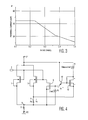
- Fig. 3 is a diagram of load current versus load resistance that illustrates the current limiting feature of the circuit of Fig. 2;
- Fig. 4 shows a second embodiment of the invention in which the current limit decreases as the temperature increases;
- Fig. 5 illustrates a third embodiment of the invention which provides a power limiting function.
- In the various figures of the drawings, elements which are the same are provided with the same reference labels. The known current limit circuit of Fig. 1 has already been described above.
- Fig. 2 shows a first embodiment of a high side intelligent power switch containing the current limit feature of the present invention. A battery or other voltage source (not shown) has a first terminal connected to the
first voltage terminal 31 and a second terminal connected to thesecond voltage terminal 32 and to a point of reference voltage, for example, ground. The high side switch, i.e.power MOSFET 1, and theload 2 are connected in a first series circuit between thevoltage terminals sense MOSFET 3, thesense resistor 4 and theload 2 are connected in a second series circuit betweenterminals circuit junction point 5 is present betweensense resistor 4,load 2 and the source electrode ofpower MOS transistor 1. - A
first NMOS transistor 6, i.e. a pull-down transistor, is connected between the inputgate drive terminal 7 and thejunction point 5. The gate electrodes of theMOS transistors gate drive terminal 7. - A bias
current source 11 and asecond NMOS transistor 12 are connected in a third series circuit between the supply voltage terminal 10 and a secondcircuit junction point 13 located between the source of thesense MOS transistor 3 and the top terminal ofsense resistor 4. The drain ofNMOS transistor 12 is directly connected to its gate and the gate oftransistor 12 is connected via a reference resistor 14 (Rref) to the gate of the pull-down MOSFET 6. The gate of theNMOS transistor 6 is connected to thecircuit junction point 5 via a source of reference current 15 through which flows a reference current, Iref. A reference voltage, Vr, is developed acrossresistor 14 which thus functions as a source of reference voltage. - In operation, the sense transistor is arranged to carry a fraction of the current flowing through the high side
power switch transistor 1. As a result, the resistance Rs of thesense resistor 4 can be chosen to have a low value so that thetransistors power MOS transistor 1. - By means of the feedback circuit comprising the
NMOS transistor 12 and thereference resistor 14, the voltage Vs across thesense resistor 4 of resistance Rs is shifted up in value by the gate/source voltage, Vgs (Tr12) oftransistor 12, and is then shifted down in value by a well defined reference voltage (V,) developed acrossreference resistor 14 so as to derive the following gatesource voltage, Vgs (Tr6) of the pull-down transistor 6,
- If the current flowing through the
power MOSFET 1 increases, so does the current flow through thesense MOSFET 3, and if it increases to a value such that the voltage drop Vs across thesense resistor 4 becomes equal to the reference voltage V, across thereference resistor 14, i.e. when Vs = Vr, then from equation (1) we get:
- The
NMOS transistors Transistor 12 is biased so that Vgs(Tr12) is slightly above the threshold voltage (Vth) of an NMOS transistor. Thus, no current limiting occurs as long as Vgs(Tr6) < Vgs(Tr12). - As mentioned above, current limiting occurs when:

- At this point, Vgs(Tr6) = Vgs(Tr12) so that the gate to source voltage, Vgs(Tr6), of
NMOS transistor 6 is sufficient to turn on thetransistor 6 which in turn pulls down the gate voltage of thepower MOS transistor 1. This prevents any further increase in the current flow through thepower transistor 1. - Since the reference voltage (Vr) is a well defined reference voltage, which may also be generated by means of a band gap reference voltage, a very accurate current limit value is achieved which, at the same time, is independent of threshold voltage variations.
- If N = (W/L of MOSFET 1)/(W/L of MOSFET 3), then the current limit value Ip (limit) of
power transistor 1 is given by:
sense resistor 4. - If both N and Rs have fixed values, which is customary, then from equation (4) the current limit is directly controlled by the reference voltage, Vr.
- The reference voltage, Vr = Iref,*Rref, where Iref and Rref are the values of the reference current in the reference
current source 15 and the resistance of thereference resistor 14, respectively. - In order to produce a very accurate reference voltage, the current Iref can be generated by means of a temperature stable bandgap voltage, Vbgap.
- As an example, if Iref = 10 µA and Rref = 50K, then V, = 0.5V. And if Rs = 10Ω and N = 1000, then Ip (limit) = (0.5/10)*1000 = 50A.
- Figure 3 shows the relationship between the current (Ip) in the
power MOSFET 1 in amps versus the load resistance Rload in ohms for the current limit circuit of Fig. 2. As can be seen from this figure, the current Ip increases up to a value of 50A as the load resistance decreases. The current Ip is thereafter limited to the value 50A despite a further decrease in the load resistance. - In the current limit circuit of Fig. 2, the
sense MOS transistor 3 carries a fraction of the current (Ip) of thepower MOS transistor 1. As a result, the voltage Vs across thesense resistor 4 is proportional to the current Ip. The sense voltage Vs across theresistor 4 is voltage level shifted upwards by theNMOS transistor 12 and the reference voltage, Vr, is subtracted therefrom to derive the gate voltage of NMOS pull-down transistor 6. The voltage Vgs (Tr12) effectively offsets the threshold voltage (Vth) which makes it possible to keep the voltage Vs as small as possible, thereby allowing the sense resistor current Is to maintain its proportionality to the power transistor current Ip. - During normal operation of the circuit, that is prior to any current limit action, Vgs (Tr12) < Vgs -(Tr6) so that the pull-
down transistor 6 is nonconductive. If the current Ip flowing throughsense resistor 4 increases to the point where Vs = Vr, Vgs(Tr6) = Vgs(Tr12) and the current limit operation commences as pull=downtransistor 6 is turned on. - The current limit circuit thus provides an accurate current limit independent of any variation of threshold voltage by using a single stage feedback mechanism which is inherently very stable without the use of any compensation. If the resistance Rs of the
sense resistor 4 increases with temperature, then from the relationship (4) it is apparent that the limit current would decrease with an increase in temperature. A range of values can be chosen for Rs, Vr and N so as to provide different current limit values. - There is another possibility to add the feature that the current limit point decreases as the temperature increases thereby to better protect the
power transistor 1. To this end, in the circuit of Fig. 2 the reference voltage, Vr, is made to decrease as the temperature increases. This can be achieved by substituting a proportional to absolute temperature (PTAT) current source is substituted for the fixed referencecurrent source 15 of Fig. 2. The PTAT current source produces a current (IPTAT) which decreases as the temperature increases. The reference voltage, Vr, is thus, Vr = IPTAT*Rref. - As a result, the reference voltage (Vr) developed across the
reference resistor 14 decreases with increasing temperature and thereby reduces the current limit value of Ip in accordance with equation (4) above. The modified current limit circuit of Figure 2 thus decreases the limiting current value as the temperature of the chip increases. This decrease is determined by the well controlled temperature dependence characteristic of the PTAT current source. The modified temperature responsive current limit circuit otherwise operates in a manner similar to that of the original current limit circuit of Fig. 2. - Fig. 4 shows still another current limit circuit in which the current limit value decreases with an increase in temperature and in a well controlled manner. The current limit circuit of Fig. 4 is similar to that of Fig. 2, except that now the
reference resistor 14 of Fig. 2 is replaced by an NPNbipolar transistor 16 having its collector connected to the firstsupply voltage terminal 31, its emitter connected to the gate of the pull-down NMOS transistor 6 and its base connected to the gate of theNMOS transistor 12. In the circuit of Fig. 4, the reference voltage, Vr, is implemented by the base/emitter voltage drop, Vbe, of thebipolar transistor 16. The Vbe voltage of theNPN transistor 16 decreases as the temperature increases. Thus, the current limit value of the current limit circuit of Fig. 4 decreases in a well controlled manner as the temperature increases. This current limit circuit functions in a similar manner to that of Fig. 2. - Fig. 5 shows a variation of the Fig. 2 circuit which provides a power limit function. The circuit is similar to the circuit of Fig. 2 except that a series circuit consisting of a
zener diode 17 and a current limitingresistor 18 are connected in parallel with the biascurrent source 11. - In this circuit, the power limiting function is implemented by decreasing the current limit value when the battery voltage at
terminal 31 increases. This circuit operates similarly to the circuit of Fig. 2 except that when the battery voltage increases above a given value, the zener diode breaks down so that a current flows through thelimit resistor 18 intotransistor 12. This additional current flowing intotransistor 12 increases as the battery voltage atterminal 31 increases. This in turn causes the gate to source voltage, Vgs(Tr12), oftransistor 12 to increase as the battery voltage increases. - Looking again at equation (1)

transistor 6, Vgs(Tr6), in order for it to pull down the gate of thepower MOS transistor 1, and thus to limit the current (Ip) is a fixed quantity. Since the gate/source voltage, Vgs(Tr12) oftransistor 12 now increases with increasing battery voltage, the required value of Vgs(Tr6) is reached at a lower value of the sense voltage, Vs, across thesense resistor 4. As a result, the current limiting function is activated at a lower current value when the battery voltage is higher. This achieves the desired power limiting function for the circuit of Fig. 5. The foregoing can also be seen from equation (1). Since Vgs(Tr6) and V, are fixed, if Vgs(Tr12) increases with the battery voltage, then Vs must decrease in order to maintain the equality of equation (1). - Finally, it is to be understood that the above- described arrangements are only illustrative of the principles of the present invention. In accordance with these principles, numerous modifications and alternatives may be devised by those skilled in the art without departing from the spirit and scope of the invention.
Claims (11)
characterized in that a feedback circuit is connected between a junction point of the sense transistor and the sense resistor and a control electrode of the further transistor, said feedback circuit including a series connection of a semiconductor device and a reference voltage source which together produce a voltage level shift.
Applications Claiming Priority (2)
| Application Number | Priority Date | Filing Date | Title |
|---|---|---|---|
| US07/987,892 US5272392A (en) | 1992-12-04 | 1992-12-04 | Current limited power semiconductor device |
| US987892 | 1992-12-04 |
Publications (3)
| Publication Number | Publication Date |
|---|---|
| EP0602699A2 true EP0602699A2 (en) | 1994-06-22 |
| EP0602699A3 EP0602699A3 (en) | 1995-01-04 |
| EP0602699B1 EP0602699B1 (en) | 1997-02-12 |
Family
ID=25533668
Family Applications (1)
| Application Number | Title | Priority Date | Filing Date |
|---|---|---|---|
| EP93203318A Expired - Lifetime EP0602699B1 (en) | 1992-12-04 | 1993-11-26 | Current limited power semiconductor device |
Country Status (4)
| Country | Link |
|---|---|
| US (1) | US5272392A (en) |
| EP (1) | EP0602699B1 (en) |
| JP (1) | JPH06217453A (en) |
| DE (1) | DE69308112T2 (en) |
Cited By (2)
| Publication number | Priority date | Publication date | Assignee | Title |
|---|---|---|---|---|
| EP0881769A2 (en) * | 1997-05-30 | 1998-12-02 | Nec Corporation | Abnormal current detection circuit and load drive circuit including the same |
| FR2824301A1 (en) * | 2001-04-18 | 2002-11-08 | Koito Mfg Co Ltd | LIGHTING DIRECTION CONTROL UNIT OF A VEHICLE HEADLIGHT, AND ITS POWER SUPPLY |
Families Citing this family (60)
| Publication number | Priority date | Publication date | Assignee | Title |
|---|---|---|---|---|
| US5500619A (en) * | 1992-03-18 | 1996-03-19 | Fuji Electric Co., Ltd. | Semiconductor device |
| JP2837054B2 (en) * | 1992-09-04 | 1998-12-14 | 三菱電機株式会社 | Insulated gate semiconductor device |
| FR2697115B1 (en) * | 1992-10-21 | 1995-01-06 | Sgs Thomson Microelectronics | Load detection circuit open. |
| DE4237122C2 (en) * | 1992-11-03 | 1996-12-12 | Texas Instruments Deutschland | Circuit arrangement for monitoring the drain current of a metal oxide semiconductor field effect transistor |
| JP3363980B2 (en) * | 1993-01-27 | 2003-01-08 | 三星電子株式会社 | Base current control circuit for output transistor and output drive stage circuit for electronic device |
| DE4305038C2 (en) * | 1993-02-18 | 1998-02-05 | Siemens Ag | MOSFET with temperature protection |
| US5406130A (en) * | 1993-08-09 | 1995-04-11 | Micrel, Inc. | Current driver with shutdown circuit |
| JP3243902B2 (en) * | 1993-09-17 | 2002-01-07 | 株式会社日立製作所 | Semiconductor device |
| GB9423076D0 (en) * | 1994-10-12 | 1995-01-04 | Philips Electronics Uk Ltd | A protected switch |
| GB9420572D0 (en) * | 1994-10-12 | 1994-11-30 | Philips Electronics Uk Ltd | A protected switch |
| JPH08154022A (en) * | 1994-11-29 | 1996-06-11 | Nec Corp | Amplifier circuit with overcurrent protecting circuit |
| DE69533308T2 (en) * | 1995-05-16 | 2004-11-25 | Stmicroelectronics S.R.L., Agrate Brianza | Method and associated circuit for detecting a circuit break |
| US5684663A (en) * | 1995-09-29 | 1997-11-04 | Motorola, Inc. | Protection element and method for protecting a circuit |
| US5631548A (en) * | 1995-10-30 | 1997-05-20 | Motorola, Inc. | Power off-loading circuit and method for dissipating power |
| US5774013A (en) * | 1995-11-30 | 1998-06-30 | Rockwell Semiconductor Systems, Inc. | Dual source for constant and PTAT current |
| JP3149773B2 (en) * | 1996-03-18 | 2001-03-26 | 富士電機株式会社 | Insulated gate bipolar transistor with current limiting circuit |
| JPH09331625A (en) * | 1996-06-11 | 1997-12-22 | Yazaki Corp | Intelligent power switch and switching device |
| JPH1014099A (en) * | 1996-06-21 | 1998-01-16 | Nec Corp | Overcurrent detecting circuit |
| US6169439B1 (en) * | 1997-01-02 | 2001-01-02 | Texas Instruments Incorporated | Current limited power MOSFET device with improved safe operating area |
| DE19805491C1 (en) * | 1998-02-11 | 1999-08-12 | Siemens Ag | Diode circuit with ideal diode characteristic |
| DE69841936D1 (en) * | 1998-05-08 | 2010-11-25 | St Microelectronics Srl | Short-circuit protection circuit, in particular for power transistors |
| US5920452A (en) * | 1998-06-01 | 1999-07-06 | Harris Corporation | Circuit and method for protecting from overcurrent conditions and detecting an open electrical load |
| US6008585A (en) * | 1998-09-30 | 1999-12-28 | Honda Giken Kogyo Kabushiki Kaisha | Apparatus and method for preventing from a short load excessive current flow through a field effect transistor that delivers current to a daytime running light on a vehicle |
| US6060834A (en) * | 1998-09-30 | 2000-05-09 | Honda Giken Kogyo Kabushiki Kaisha | Protection from overheating of a switching transistor that delivers current to a daytime running light on a vehicle |
| US6055149A (en) * | 1998-12-02 | 2000-04-25 | Intersil Corporation | Current limited, thermally protected, power device |
| US6547353B2 (en) | 1999-07-27 | 2003-04-15 | Stmicroelectronics, Inc. | Thermal ink jet printhead system with multiple output driver circuit for powering heating element and associated method |
| US6603358B2 (en) * | 2000-08-23 | 2003-08-05 | Intersil Americas Inc. | Integrated circuit with current-limited power output and associated method |
| ITVA20000031A1 (en) * | 2000-09-07 | 2002-03-07 | St Microelectronics Srl | DETECTION OF THE CURRENT DELIVERED TO A LOAD. |
| DE10147882B4 (en) * | 2001-09-28 | 2005-06-23 | Infineon Technologies Ag | Half-bridge circuit and method for its control |
| US6600362B1 (en) | 2002-02-08 | 2003-07-29 | Toko, Inc. | Method and circuits for parallel sensing of current in a field effect transistor (FET) |
| JP3681374B2 (en) * | 2002-12-19 | 2005-08-10 | 株式会社日立製作所 | Current detection device and PWM inverter using the same |
| US6970337B2 (en) * | 2003-06-24 | 2005-11-29 | Linear X Systems Inc. | High-voltage low-distortion input protection current limiter |
| JP4068022B2 (en) * | 2003-07-16 | 2008-03-26 | Necエレクトロニクス株式会社 | Overcurrent detection circuit and load drive circuit |
| JP4401178B2 (en) * | 2004-01-27 | 2010-01-20 | Necエレクトロニクス株式会社 | Output transistor current limit circuit |
| EP1653619A1 (en) * | 2004-10-27 | 2006-05-03 | St Microelectronics S.A. | Protection of a power transistor |
| EP1852766B1 (en) * | 2005-02-24 | 2010-11-24 | Fujitsu Ltd. | Reference voltage generating circuit |
| US7554152B1 (en) | 2006-01-11 | 2009-06-30 | National Semiconductor Corporation | Versatile system for integrated sense transistor |
| US7336085B2 (en) * | 2006-02-17 | 2008-02-26 | Infineon Technologies Ag | Current sensing circuit |
| US7869177B2 (en) * | 2006-07-19 | 2011-01-11 | Hewlett-Packard Development Company, L.P. | Detection circuitry |
| US7672102B2 (en) * | 2006-12-31 | 2010-03-02 | Texas Instruments Incorporated | Electrical overstress protection |
| US7710701B1 (en) * | 2007-04-09 | 2010-05-04 | National Semiconductor Corporation | System and method for providing a process, temperature and over-drive invariant over-current protection circuit |
| JP2009277930A (en) * | 2008-05-15 | 2009-11-26 | Nec Electronics Corp | Semiconductor device |
| US20090295369A1 (en) * | 2008-06-02 | 2009-12-03 | Yang Doris | Current sensing circuit |
| US8203276B2 (en) * | 2008-11-28 | 2012-06-19 | Lightech Electronic Industries Ltd. | Phase controlled dimming LED driver system and method thereof |
| US9167641B2 (en) * | 2008-11-28 | 2015-10-20 | Lightech Electronic Industries Ltd. | Phase controlled dimming LED driver system and method thereof |
| JP5266084B2 (en) * | 2009-02-17 | 2013-08-21 | ルネサスエレクトロニクス株式会社 | Overcurrent protection circuit |
| US7852148B2 (en) * | 2009-03-27 | 2010-12-14 | Semiconductor Components Industries, Llc | Method of forming a sensing circuit and structure therefor |
| WO2010137158A1 (en) | 2009-05-28 | 2010-12-02 | トヨタ自動車株式会社 | Semiconductor device |
| US8004350B2 (en) * | 2009-06-03 | 2011-08-23 | Infineon Technologies Ag | Impedance transformation with transistor circuits |
| JP5352500B2 (en) * | 2010-03-02 | 2013-11-27 | ルネサスエレクトロニクス株式会社 | Semiconductor device |
| JP5969237B2 (en) * | 2012-03-23 | 2016-08-17 | エスアイアイ・セミコンダクタ株式会社 | Semiconductor device |
| US9564796B1 (en) | 2014-01-15 | 2017-02-07 | Western Digital Technologies, Inc. | Power circuit with overvoltage protection |
| JP6353268B2 (en) * | 2014-05-07 | 2018-07-04 | ローム株式会社 | Overcurrent protection circuit and power supply device using the same |
| US9791881B2 (en) * | 2014-07-22 | 2017-10-17 | Infineon Technologies Austria Ag | Self-driven synchronous rectification for a power converter |
| US9602032B2 (en) * | 2014-09-26 | 2017-03-21 | Electronics And Telecommunications Research Institute | BLDC motor system including parameter detecting circuit and operating method thereof |
| US9653912B2 (en) * | 2014-12-16 | 2017-05-16 | Nxp B.V. | Inrush current limiter |
| JP6520102B2 (en) * | 2014-12-17 | 2019-05-29 | 富士電機株式会社 | Semiconductor device and current limiting method |
| US10394259B2 (en) | 2015-08-28 | 2019-08-27 | Stmicroelectronics S.R.L. | Current limiting electronic fuse circuit |
| DE102019104297A1 (en) * | 2018-02-20 | 2019-08-22 | Maxim Integrated Products, Inc. | Current measuring devices and associated methods |
| EP3812873A1 (en) * | 2019-10-24 | 2021-04-28 | NXP USA, Inc. | Voltage reference generation with compensation for temperature variation |
Citations (5)
| Publication number | Priority date | Publication date | Assignee | Title |
|---|---|---|---|---|
| DE3402341A1 (en) * | 1983-01-31 | 1984-08-02 | Sgs-Ates Componenti Elettronici S.P.A., Agrate Brianza, Mailand/Milano | PROTECTIVE DEVICE FOR A POWER ELEMENT OF AN INTEGRATED CIRCUIT |
| JPS6468005A (en) * | 1987-09-09 | 1989-03-14 | Nissan Motor | Mosfet incorporating protection function |
| EP0425035A2 (en) * | 1989-10-23 | 1991-05-02 | Koninklijke Philips Electronics N.V. | Overload protection drive circuit for a power transistor |
| EP0492375A1 (en) * | 1990-12-20 | 1992-07-01 | STMicroelectronics S.r.l. | Voltage/current characteristics control circuit particularly for protecting power transistors |
| EP0571302A1 (en) * | 1992-05-18 | 1993-11-24 | STMicroelectronics S.A. | Amplifier with limited output current |
Family Cites Families (2)
| Publication number | Priority date | Publication date | Assignee | Title |
|---|---|---|---|---|
| US5184272A (en) * | 1989-03-31 | 1993-02-02 | Hitachi, Ltd. | High-side switch with overcurrent protecting circuit |
| US5061863A (en) * | 1989-05-16 | 1991-10-29 | Kabushiki Kaisha Toyoda Jidoshokki Seisakusho | Transistor provided with a current detecting function |
-
1992
- 1992-12-04 US US07/987,892 patent/US5272392A/en not_active Expired - Fee Related
-
1993
- 1993-11-26 DE DE69308112T patent/DE69308112T2/en not_active Expired - Fee Related
- 1993-11-26 EP EP93203318A patent/EP0602699B1/en not_active Expired - Lifetime
- 1993-12-01 JP JP5301681A patent/JPH06217453A/en active Pending
Patent Citations (5)
| Publication number | Priority date | Publication date | Assignee | Title |
|---|---|---|---|---|
| DE3402341A1 (en) * | 1983-01-31 | 1984-08-02 | Sgs-Ates Componenti Elettronici S.P.A., Agrate Brianza, Mailand/Milano | PROTECTIVE DEVICE FOR A POWER ELEMENT OF AN INTEGRATED CIRCUIT |
| JPS6468005A (en) * | 1987-09-09 | 1989-03-14 | Nissan Motor | Mosfet incorporating protection function |
| EP0425035A2 (en) * | 1989-10-23 | 1991-05-02 | Koninklijke Philips Electronics N.V. | Overload protection drive circuit for a power transistor |
| EP0492375A1 (en) * | 1990-12-20 | 1992-07-01 | STMicroelectronics S.r.l. | Voltage/current characteristics control circuit particularly for protecting power transistors |
| EP0571302A1 (en) * | 1992-05-18 | 1993-11-24 | STMicroelectronics S.A. | Amplifier with limited output current |
Non-Patent Citations (1)
| Title |
|---|
| PATENT ABSTRACTS OF JAPAN, unexamined applications, E section, vol. 13, no. 285, June 29, 1989 THE PATENT OFFICE JAPANESE GOVERNMENT page 4 E 780; & JP-A-01 068 005 (NISSAN) * |
Cited By (3)
| Publication number | Priority date | Publication date | Assignee | Title |
|---|---|---|---|---|
| EP0881769A2 (en) * | 1997-05-30 | 1998-12-02 | Nec Corporation | Abnormal current detection circuit and load drive circuit including the same |
| EP0881769A3 (en) * | 1997-05-30 | 2000-05-17 | Nec Corporation | Abnormal current detection circuit and load drive circuit including the same |
| FR2824301A1 (en) * | 2001-04-18 | 2002-11-08 | Koito Mfg Co Ltd | LIGHTING DIRECTION CONTROL UNIT OF A VEHICLE HEADLIGHT, AND ITS POWER SUPPLY |
Also Published As
| Publication number | Publication date |
|---|---|
| EP0602699A3 (en) | 1995-01-04 |
| EP0602699B1 (en) | 1997-02-12 |
| DE69308112D1 (en) | 1997-03-27 |
| JPH06217453A (en) | 1994-08-05 |
| DE69308112T2 (en) | 1997-07-31 |
| US5272392A (en) | 1993-12-21 |
Similar Documents
| Publication | Publication Date | Title |
|---|---|---|
| EP0602699B1 (en) | Current limited power semiconductor device | |
| US5245523A (en) | Power delivery circuit with current detection | |
| US4800331A (en) | Linear current limiter with temperature shutdown | |
| US7924084B2 (en) | Semiconductor device | |
| EP0241785B1 (en) | Output driver circuit | |
| CA1211789A (en) | Electronic circuit breaker | |
| US4495536A (en) | Voltage transient protection circuit | |
| US20060028267A1 (en) | Semiconductor integrated circuit device | |
| JPH0654866B2 (en) | Electronic control circuit having input / output terminals | |
| US8035943B2 (en) | Protection circuit apparatus | |
| US6650520B2 (en) | Power supply reverse bias protection circuit for protecting both analog and digital devices coupled thereto | |
| JP3427436B2 (en) | Drive circuit | |
| US6465999B2 (en) | Current-limited switch with fast transient response | |
| US4884161A (en) | Integrated circuit voltage regulator with transient protection | |
| US5886543A (en) | Power semiconductor switch having a load open-circuit detection circuit | |
| US5221888A (en) | Current limited temperature responsive circuit | |
| JPH03166816A (en) | Semiconductor integrated circuit device | |
| EP1401077B1 (en) | A circuit for protection against polarity reversal in the supply of an electric circuit | |
| WO1998032226A1 (en) | Low current drain switch interface circuit | |
| US20230411947A1 (en) | Intelligent semiconductor switch | |
| US11552629B1 (en) | Semiconductor device and manufacturing method thereof | |
| JPH08289458A (en) | Overcurrent protective circuit | |
| GB2217938A (en) | Current sensing circuit | |
| GB1604435A (en) | Electrical circuit with load continuity detector | |
| GB2234871A (en) | Power delivery circuit with over current detection |
Legal Events
| Date | Code | Title | Description |
|---|---|---|---|
| PUAI | Public reference made under article 153(3) epc to a published international application that has entered the european phase |
Free format text: ORIGINAL CODE: 0009012 |
|
| AK | Designated contracting states |
Kind code of ref document: A2 Designated state(s): DE FR GB IT |
|
| RAP1 | Party data changed (applicant data changed or rights of an application transferred) |
Owner name: N.V. PHILIPS' GLOEILAMPENFABRIEKEN |
|
| PUAL | Search report despatched |
Free format text: ORIGINAL CODE: 0009013 |
|
| RHK1 | Main classification (correction) |
Ipc: H02H 7/20 |
|
| AK | Designated contracting states |
Kind code of ref document: A3 Designated state(s): DE FR GB IT |
|
| 17P | Request for examination filed |
Effective date: 19950704 |
|
| GRAG | Despatch of communication of intention to grant |
Free format text: ORIGINAL CODE: EPIDOS AGRA |
|
| 17Q | First examination report despatched |
Effective date: 19960119 |
|
| GRAH | Despatch of communication of intention to grant a patent |
Free format text: ORIGINAL CODE: EPIDOS IGRA |
|
| GRAH | Despatch of communication of intention to grant a patent |
Free format text: ORIGINAL CODE: EPIDOS IGRA |
|
| GRAA | (expected) grant |
Free format text: ORIGINAL CODE: 0009210 |
|
| AK | Designated contracting states |
Kind code of ref document: B1 Designated state(s): DE FR GB IT |
|
| REF | Corresponds to: |
Ref document number: 69308112 Country of ref document: DE Date of ref document: 19970327 |
|
| ITF | It: translation for a ep patent filed |
Owner name: 0508;06MIFING. C. GREGORJ S.P.A. |
|
| ET | Fr: translation filed | ||
| PLBE | No opposition filed within time limit |
Free format text: ORIGINAL CODE: 0009261 |
|
| STAA | Information on the status of an ep patent application or granted ep patent |
Free format text: STATUS: NO OPPOSITION FILED WITHIN TIME LIMIT |
|
| 26N | No opposition filed | ||
| REG | Reference to a national code |
Ref country code: FR Ref legal event code: CD |
|
| REG | Reference to a national code |
Ref country code: GB Ref legal event code: IF02 |
|
| PGFP | Annual fee paid to national office [announced via postgrant information from national office to epo] |
Ref country code: FR Payment date: 20021125 Year of fee payment: 10 |
|
| PGFP | Annual fee paid to national office [announced via postgrant information from national office to epo] |
Ref country code: GB Payment date: 20021129 Year of fee payment: 10 |
|
| PGFP | Annual fee paid to national office [announced via postgrant information from national office to epo] |
Ref country code: DE Payment date: 20030118 Year of fee payment: 10 |
|
| PG25 | Lapsed in a contracting state [announced via postgrant information from national office to epo] |
Ref country code: GB Free format text: LAPSE BECAUSE OF NON-PAYMENT OF DUE FEES Effective date: 20031126 |
|
| PG25 | Lapsed in a contracting state [announced via postgrant information from national office to epo] |
Ref country code: DE Free format text: LAPSE BECAUSE OF NON-PAYMENT OF DUE FEES Effective date: 20040602 |
|
| GBPC | Gb: european patent ceased through non-payment of renewal fee |
Effective date: 20031126 |
|
| PG25 | Lapsed in a contracting state [announced via postgrant information from national office to epo] |
Ref country code: FR Free format text: LAPSE BECAUSE OF NON-PAYMENT OF DUE FEES Effective date: 20040730 |
|
| REG | Reference to a national code |
Ref country code: FR Ref legal event code: ST |
|
| PG25 | Lapsed in a contracting state [announced via postgrant information from national office to epo] |
Ref country code: IT Free format text: LAPSE BECAUSE OF NON-PAYMENT OF DUE FEES;WARNING: LAPSES OF ITALIAN PATENTS WITH EFFECTIVE DATE BEFORE 2007 MAY HAVE OCCURRED AT ANY TIME BEFORE 2007. THE CORRECT EFFECTIVE DATE MAY BE DIFFERENT FROM THE ONE RECORDED. Effective date: 20051126 |