EP0600522A2 - Convertisseur de tension avec circuit intermédiaire à haute fréquence - Google Patents
Convertisseur de tension avec circuit intermédiaire à haute fréquence Download PDFInfo
- Publication number
- EP0600522A2 EP0600522A2 EP93119915A EP93119915A EP0600522A2 EP 0600522 A2 EP0600522 A2 EP 0600522A2 EP 93119915 A EP93119915 A EP 93119915A EP 93119915 A EP93119915 A EP 93119915A EP 0600522 A2 EP0600522 A2 EP 0600522A2
- Authority
- EP
- European Patent Office
- Prior art keywords
- transistor
- voltage
- capacitor
- semiconductor switch
- power
- Prior art date
- Legal status (The legal status is an assumption and is not a legal conclusion. Google has not performed a legal analysis and makes no representation as to the accuracy of the status listed.)
- Withdrawn
Links
Images




Classifications
-
- H—ELECTRICITY
- H02—GENERATION; CONVERSION OR DISTRIBUTION OF ELECTRIC POWER
- H02M—APPARATUS FOR CONVERSION BETWEEN AC AND AC, BETWEEN AC AND DC, OR BETWEEN DC AND DC, AND FOR USE WITH MAINS OR SIMILAR POWER SUPPLY SYSTEMS; CONVERSION OF DC OR AC INPUT POWER INTO SURGE OUTPUT POWER; CONTROL OR REGULATION THEREOF
- H02M3/00—Conversion of DC power input into DC power output
- H02M3/22—Conversion of DC power input into DC power output with intermediate conversion into AC
- H02M3/24—Conversion of DC power input into DC power output with intermediate conversion into AC by static converters
- H02M3/28—Conversion of DC power input into DC power output with intermediate conversion into AC by static converters using discharge tubes with control electrode or semiconductor devices with control electrode to produce the intermediate AC
- H02M3/325—Conversion of DC power input into DC power output with intermediate conversion into AC by static converters using discharge tubes with control electrode or semiconductor devices with control electrode to produce the intermediate AC using devices of a triode or a transistor type requiring continuous application of a control signal
- H02M3/335—Conversion of DC power input into DC power output with intermediate conversion into AC by static converters using discharge tubes with control electrode or semiconductor devices with control electrode to produce the intermediate AC using devices of a triode or a transistor type requiring continuous application of a control signal using semiconductor devices only
- H02M3/337—Conversion of DC power input into DC power output with intermediate conversion into AC by static converters using discharge tubes with control electrode or semiconductor devices with control electrode to produce the intermediate AC using devices of a triode or a transistor type requiring continuous application of a control signal using semiconductor devices only in push-pull configuration
- H02M3/3376—Conversion of DC power input into DC power output with intermediate conversion into AC by static converters using discharge tubes with control electrode or semiconductor devices with control electrode to produce the intermediate AC using devices of a triode or a transistor type requiring continuous application of a control signal using semiconductor devices only in push-pull configuration with automatic control of output voltage or current
-
- H—ELECTRICITY
- H02—GENERATION; CONVERSION OR DISTRIBUTION OF ELECTRIC POWER
- H02M—APPARATUS FOR CONVERSION BETWEEN AC AND AC, BETWEEN AC AND DC, OR BETWEEN DC AND DC, AND FOR USE WITH MAINS OR SIMILAR POWER SUPPLY SYSTEMS; CONVERSION OF DC OR AC INPUT POWER INTO SURGE OUTPUT POWER; CONTROL OR REGULATION THEREOF
- H02M3/00—Conversion of DC power input into DC power output
- H02M3/22—Conversion of DC power input into DC power output with intermediate conversion into AC
- H02M3/24—Conversion of DC power input into DC power output with intermediate conversion into AC by static converters
- H02M3/28—Conversion of DC power input into DC power output with intermediate conversion into AC by static converters using discharge tubes with control electrode or semiconductor devices with control electrode to produce the intermediate AC
- H02M3/325—Conversion of DC power input into DC power output with intermediate conversion into AC by static converters using discharge tubes with control electrode or semiconductor devices with control electrode to produce the intermediate AC using devices of a triode or a transistor type requiring continuous application of a control signal
- H02M3/335—Conversion of DC power input into DC power output with intermediate conversion into AC by static converters using discharge tubes with control electrode or semiconductor devices with control electrode to produce the intermediate AC using devices of a triode or a transistor type requiring continuous application of a control signal using semiconductor devices only
- H02M3/33569—Conversion of DC power input into DC power output with intermediate conversion into AC by static converters using discharge tubes with control electrode or semiconductor devices with control electrode to produce the intermediate AC using devices of a triode or a transistor type requiring continuous application of a control signal using semiconductor devices only having several active switching elements
- H02M3/33571—Half-bridge at primary side of an isolation transformer
-
- H—ELECTRICITY
- H02—GENERATION; CONVERSION OR DISTRIBUTION OF ELECTRIC POWER
- H02M—APPARATUS FOR CONVERSION BETWEEN AC AND AC, BETWEEN AC AND DC, OR BETWEEN DC AND DC, AND FOR USE WITH MAINS OR SIMILAR POWER SUPPLY SYSTEMS; CONVERSION OF DC OR AC INPUT POWER INTO SURGE OUTPUT POWER; CONTROL OR REGULATION THEREOF
- H02M7/00—Conversion of AC power input into DC power output; Conversion of DC power input into AC power output
- H02M7/42—Conversion of DC power input into AC power output without possibility of reversal
- H02M7/44—Conversion of DC power input into AC power output without possibility of reversal by static converters
- H02M7/48—Conversion of DC power input into AC power output without possibility of reversal by static converters using discharge tubes with control electrode or semiconductor devices with control electrode
- H02M7/53—Conversion of DC power input into AC power output without possibility of reversal by static converters using discharge tubes with control electrode or semiconductor devices with control electrode using devices of a triode or transistor type requiring continuous application of a control signal
- H02M7/537—Conversion of DC power input into AC power output without possibility of reversal by static converters using discharge tubes with control electrode or semiconductor devices with control electrode using devices of a triode or transistor type requiring continuous application of a control signal using semiconductor devices only, e.g. single switched pulse inverters
- H02M7/538—Conversion of DC power input into AC power output without possibility of reversal by static converters using discharge tubes with control electrode or semiconductor devices with control electrode using devices of a triode or transistor type requiring continuous application of a control signal using semiconductor devices only, e.g. single switched pulse inverters in a push-pull configuration
-
- H—ELECTRICITY
- H02—GENERATION; CONVERSION OR DISTRIBUTION OF ELECTRIC POWER
- H02M—APPARATUS FOR CONVERSION BETWEEN AC AND AC, BETWEEN AC AND DC, OR BETWEEN DC AND DC, AND FOR USE WITH MAINS OR SIMILAR POWER SUPPLY SYSTEMS; CONVERSION OF DC OR AC INPUT POWER INTO SURGE OUTPUT POWER; CONTROL OR REGULATION THEREOF
- H02M7/00—Conversion of AC power input into DC power output; Conversion of DC power input into AC power output
- H02M7/42—Conversion of DC power input into AC power output without possibility of reversal
- H02M7/44—Conversion of DC power input into AC power output without possibility of reversal by static converters
- H02M7/48—Conversion of DC power input into AC power output without possibility of reversal by static converters using discharge tubes with control electrode or semiconductor devices with control electrode
- H02M7/53—Conversion of DC power input into AC power output without possibility of reversal by static converters using discharge tubes with control electrode or semiconductor devices with control electrode using devices of a triode or transistor type requiring continuous application of a control signal
- H02M7/537—Conversion of DC power input into AC power output without possibility of reversal by static converters using discharge tubes with control electrode or semiconductor devices with control electrode using devices of a triode or transistor type requiring continuous application of a control signal using semiconductor devices only, e.g. single switched pulse inverters
- H02M7/5387—Conversion of DC power input into AC power output without possibility of reversal by static converters using discharge tubes with control electrode or semiconductor devices with control electrode using devices of a triode or transistor type requiring continuous application of a control signal using semiconductor devices only, e.g. single switched pulse inverters in a bridge configuration
-
- H—ELECTRICITY
- H03—ELECTRONIC CIRCUITRY
- H03K—PULSE TECHNIQUE
- H03K17/00—Electronic switching or gating, i.e. not by contact-making and –breaking
- H03K17/51—Electronic switching or gating, i.e. not by contact-making and –breaking characterised by the components used
- H03K17/56—Electronic switching or gating, i.e. not by contact-making and –breaking characterised by the components used by the use, as active elements, of semiconductor devices
- H03K17/687—Electronic switching or gating, i.e. not by contact-making and –breaking characterised by the components used by the use, as active elements, of semiconductor devices the devices being field-effect transistors
- H03K17/6871—Electronic switching or gating, i.e. not by contact-making and –breaking characterised by the components used by the use, as active elements, of semiconductor devices the devices being field-effect transistors the output circuit comprising more than one controlled field-effect transistor
-
- H—ELECTRICITY
- H02—GENERATION; CONVERSION OR DISTRIBUTION OF ELECTRIC POWER
- H02M—APPARATUS FOR CONVERSION BETWEEN AC AND AC, BETWEEN AC AND DC, OR BETWEEN DC AND DC, AND FOR USE WITH MAINS OR SIMILAR POWER SUPPLY SYSTEMS; CONVERSION OF DC OR AC INPUT POWER INTO SURGE OUTPUT POWER; CONTROL OR REGULATION THEREOF
- H02M3/00—Conversion of DC power input into DC power output
- H02M3/01—Resonant DC/DC converters
Definitions
- This invention relates to a power buffer for a voltage converter and particularly relates to the use of a high frequency converter for converting either a high A.C. voltage signal or a high level D.C. voltage to a low level D.C. voltage.
- Many different types of electrical devices are powered by low voltage systems. Such devices include, but are not limited to, household and kitchen products, power tools, outdoor lawn and garden equipment, lighting systems, camping accessories, automotive products and a variety of battery chargers. Many of these devices are operated in areas where conventional A.C. sources, or high level D.C. sources, are available. In such instances, it would be advantageous to use the available power sources to operate the devices. Consequently, facility must be provided for converting the available power source to a source and level compatible with the power operating level of the device to be used.
- Another converter system has employed a technique whereby the initial power source, either A.C. or D.C., is converted to a high frequency signal by use of a pair of alternately switched transistors. Voltage reduction is then accomplished by a high frequency transformer. The transformer output is then rectified to obtain the low level D.C. voltage for operation of a low voltage device.
- One example of such a circuit has a series leg which includes an inductor, a series capacitor and the primary of a high frequency transformer.
- One end of the series leg is connected between a pair of alternating switches such as transistors with parallel connected diodes.
- the other end of the series leg is connected between a pair of split capacitors.
- the other ends of the split capacitors and the other ends of the switches are connected across a full wave rectifier.
- This type of circuit requires the split capacitors which function as supply sources on alternate halves of the circuit operation and may require a filter capacitor. With this type of circuit, it is difficult to directly sense information which could be determined by the voltage parameter of the series capacitor. Further, it is not possible to sense directly the transformer current. Therefore, current sensing would have to be accomplished by some other indirect means such as, for example, a current transformer.
- the high frequency principle in another type of system, includes an oscillatory circuit with an inductor and a capacitor.
- the inductor is connected to the primary of a high frequency transformer or it could be a leakage inductance of the high frequency transformer.
- Oscillations developed by the oscillatory circuit control a switching means to connect a D.C. supply to the inductor which receives and stores energy from the supply.
- power may be coupled to a load circuit only during a portion of the total cycle time which results in using either a separate inductor or a transformer with substantial leakage inductance and a complex control circuit.
- the topology can't be used on a transformer with a very low leakage inductance because transient imbalance in transformer volt-seconds can permanently saturate the transformer and has to be recovered by complex control means.
- the switching transistors see excessive currents which could cause a catastrophic failure unless complex control means are used.
- Such systems include an oscillatory circuit which depends on a complex circuit design utilising many reactive components, transistors, integrated circuit chips, diodes and resistive components. While the basis for high frequency operation permits the use of a lightweight transformer, the number of discrete components and chips employed in the complex circuit design lessen significantly any space advantage gained by use of the lightweight transformer.
- a power buffer comprises a first D.C. power source; a second D.C. power source and a chargeable voltage storage device, characterised by a first switching device connectable to the first D.C. power source and the second D.C. power source, the voltage storage device and a load; a second switching device connectable to the second D.C. power source, the voltage storage device and the load; means for operating the first switching device during a first period of operation of the power buffer to supply current from the first D.C. power source to the load in a first direction and to charge the voltage storage device from the first D.C. power source and the second D.C. power source; and means for connecting the voltage storage device to the second switching device to bias the second switching device into operation during a second period of operation whereby current is supplied from the second D.C. power source to the load in a second direction.
- the operating means includes a binary generator which controls the power buffer to operate during the first period and second period of operation.
- the connecting means preferably includes a third switching device connected to the voltage storage device and to the second switching device; a fourth switching device connected to the third switching device; and means for controlling the operation of the fourth switching device: (1) to maintain the third switching device inoperative during the first period of operation of the power buffer; and (2) to facilitate operation of the third switching device during the second period of operation of the power buffer so that the second switching device is operated.
- the switching devices of the power buffer are preferably N channel power MOSFET transistors.
- the power buffer further comprises means for conducting current from the voltage storage device to the third switching device to operate the third switching device and also preferably includes means for conducting current from the voltage storage device initially rapidly through the third switching device to operate the second switching device and thereafter for conducting the current at a slower rate.
- the connecting means of the power buffer may comprise a third switching device connected to the voltage storage device and to the second switching device; means for conducting current from the voltage storage device to the third switching device to operate the third switching device; and means for conducting current from the voltage storage device initially rapidly through the third switching device to operate the second switching device and thereafter for conducting the current at a slower rate.
- the chargeable voltage storage device of the power buffer is preferably a third D.C. power source.
- FIGs 1, 3, 4, 5, 6 and collectively to Figures 7A and 7B there are illustrated six voltage converters 100, 200, 250, 300, 400 and 500, respectively. Substantial portions of the converter topology of each of power converters (100, 200, 250, 300, 400 and 500) are common to one or more of the other converters. Therefore, in those instances where an element or component is first introduced in one figure and also appears in subsequent figures, the element or component will retain in the subsequent figures the number assigned thereto in the first figure.
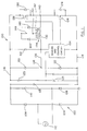
- voltage converter (100) is designed to convert either a high A.C. voltage, or a high level D.C. voltage, to a low level D.C. voltage. While more detailed schematic representations of the various preferred embodiments of the invention are illustrated in Figures 3, 4, 5, 6, 7A and 7B and will be described hereinafter, the schematic of Figure 1 represents a circuit diagram embodying the basic principles of the invention.
- parameters of the components of voltage converter (100) can be designed selectively to convert the voltage levels of a variety of A.C. and D.C. sources to desired D.C. voltage levels.
- voltage converter (100) can convert an A.C. input of 120 volts, 60 Hz, to any low level D.C. voltage such as, for example, a 12 volts D.C. output.
- voltage converter (100) can convert an A.C. input of 220 volts, 50 Hz, to any low level D.C. voltage output.
- voltage converter (100) can convert a high level D.C. voltage to a low level D.C. voltage, for example, 150 volts D.C. to 12 volts D.C.
- voltage converter (100) includes a bridge rectifier (102) formed by diodes (104, 106, 108 and 110).
- An A.C. source (112) which supplies, for example, 120 volts at 60 Hz., is connected to rectifier (102).
- A.C. source (112) functions as a primary power source for voltage converter (100).
- the output of rectifier (102) is applied between ground reference line (114) and line (116).
- the rectified output is filtered by capacitor (118) to thereby provide 150 volts D.C. between lines (114 and 116).
- a pair of oscillation damping diodes (120 and 122) are connected in series between lines (114 and 116).
- a voltage dropping resistor (123) and a voltage-establishing Zener diode (125) also are connected in series between lines (114 and 116).
- Intrinsic diodes (128 and 130) are representative of diode structure inherently formed as an integral and physical part of transistors (124 and 126), respectively, and are connected in parallel with the source and drain electrodes of the transistors.
- One side of a primary winding (132) of a high frequency, step-down transformer (134) is connected through a line (136) to a juncture (138) between diodes (120 and 122).
- the other side of primary winding (132) is connected to a node (140) between the drain electrode of transistor (124) and the source electrode of transistor (126).
- the outside terminals of a centre tapped secondary winding (142) of transformer (134) are connected to the anodes of rectifier diodes (144 and 146).
- the cathodes of diodes (144 and 146) are each connected to a first output terminal (148) of voltage converter (100) while the centre tap of secondary winding (142) is connected to a second output terminal (150).
- a load circuit could be formed solely by a single component such as, for example, primary winding (132) or could also include secondary winding (142), rectifiers (144 and 146) and output terminals (148 and 150).
- any load to be connected to any embodiment of voltage converter described herein, such as voltage converter (100), could be connected to the load circuit.
- a capacitor (152) is connected between lines (114 and 136) in parallel with diode (120).
- a sensing and control circuit designated generally by the numeral (154), also is connected between lines (114 and 136) and has outputs which are connected to the gate electrodes of transistors (124 and 126).
- Sensing and control circuit (154) includes facility for monitoring the voltage appearing across capacitor (152) and also includes a high frequency oscillator.
- the high frequency oscillator of circuit (154) functions to facilitate the alternating operation of transistors (124 and 126) during normal operation of voltage converter (100), while other portions of circuit (154) functions to facilitate the complete and simultaneous shutdown of both transistors if undesirable conditions occur such as, for example, an overload.
- A.C. voltage When A.C. voltage is applied to voltage converter (100), a D.C. voltage of 150 volts D.C. is developed between lines (114 and 116). A D.C. voltage is developed thereby across Zener diode (125) which is applied to and facilitates operation of sensing and control circuit (154) which produces an alternating voltage in the form of a square wave at a frequency of, for example, 25 KHz whereby transistors (124 and 126) are alternately operated.
- transistor (124) is biased on and current flows through capacitor (152), through primary winding (132), through the source and drain electrodes of transistor (124) and over line (114).
- the filtered output of rectifier (102) functions as a primary power source for transformer (134) whereby, as current flows in the first or charging direction through primary winding (132), a voltage is induced in secondary winding (142). If a load is connected to output terminals (148 and 150), current flows in the secondary winding (142), through one of the diodes (144 or 146), through any load connected to the output terminals and to the centre tap of the secondary winding.
- capacitor 152 charges to a specific voltage level.
- transistor (124) is turned off and transistor (126) is turned on.
- primary winding (132) is now connected in a closed series loop which includes the source and drain electrodes of transistor (126) and capacitor (152).
- capacitor (152) begins to discharge, thereby supplying current in the closed series loop. This current flows in a second or discharging direction through primary winding (132) which is in a direction opposite to that when transistor (124) was conducting.
- capacitor (152) functions as a secondary power source for transformer (134) whereby a voltage is induced in secondary winding (142). Again, assuming that a load is connected to output terminals (148 and 150), this results in current flow through the other of diodes (144 and 146), through any load connected to output terminals (148 and 150) and returns through the centre tap of transformer (134).
- 150 volts D.C. appears between lines (114 and 116).
- the voltage between lines (114 and 116) is effectively split between primary winding (132) and capacitor (152) whereby the capacitor charges, theoretically, to a level of 75 volts.
- the remaining 75 volts is applied across primary winding (132) which is then stepped down in value by the split secondary winding (142).
- the secondary winding voltage is further rectified by diodes (144 and 146) to provide a low level D.C. voltage, for example, 12 volts, which is applied to output terminals (148 and 150) and, thereby, to any load connected thereto.
- capacitor (152) is the power source for transformer (134). Since capacitor (152) has been charged to a level of 75 volts during the previous half cycle of the square wave output of circuit (154), this level of voltage effectively is applied to primary winding (132) and is the same voltage level applied to the primary winding during the previous half cycle.
- the same level of voltage is applied to primary winding (132) during alternate half cycles of the square wave output of the oscillator of circuit (154).
- a high frequency signal is applied to primary winding (132) which is stepped down by transformer (134) and rectified to provide the desired low level D.C. voltage at output terminals (148 and 150).
- transistor (124) When transistor (124) is on, current is flowing in the first or charging direction through primary winding (132) which is in a direction to charge capacitor (152).
- capacitor (152) When transistor (124) is turned off and transistor (126) is turned on, capacitor (152) is in a mode to attempt to discharge as noted above. However, because of the stored energy of primary winding (132), current will continue to flow in the first direction through the primary winding which continues to charge capacitor (152) even though transistor (126) is now in a conducting mode.
- intrinsic diode (130) is polarised to permit such current to bypass transistor (126) which is now on and biased for current conduction in the opposite or discharging direction. Due to the continued current flow in the charging direction, capacitor (152) charges to a level slightly above 75 volts. After the stored energy about primary winding (132) has fully dissipated, capacitor (152) begins to discharge as described above and current flows in the second or discharging direction through primary winding (132).
- transformer (134) Under a no-load condition, transformer (134) presents a relatively large inductance, and thereby a larger impedance, in the circuit with capacitor (152). Thus, capacitor (152) will discharge very slowly.
- transistor (126) is turned off and transistor (124) is turned on.
- current should again flow in the first or charging direction from primary winding (132) to capacitor (152).
- current continues to flow in the second or discharging direction from capacitor (152) to primary winding (132) whereby the capacitor continues to discharge at the slow rate due to the large inductance presented by transformer 134 during a no-load condition.
- current flows through intrinsic diode (128) even though transistor (124) is turned on and biased to conduct current in the opposite or charging direction.
- capacitor (152) continues to discharge, the voltage across the capacitor continues to drop to a level slightly below 75 volts.
- transformer (134) now presents a smaller inductance, and thereby less impedance, in the circuit of primary winding (132) than was presented during operation under a no-load condition.
- Sensing and control circuit (154) is designed to respond to wide swings in the voltage appearing across capacitor (152) and shut down the operation of both transistors (124 and 126). Thus, when an overload condition occurs, the voltage ripple of capacitor (152) increases significantly and beyond a predetermined level whereby transistors (124 and 126) are precluded from operating.
- sensing and control circuit (154) constantly monitors and senses the voltage appearing across capacitor (152) and controls the operation of voltage converter (100) in response to the sensed capacitor voltage.
- capacitor (152) is valued at .5 to 2.2 microfarads when voltage converter (100) operates in this mode. Capacitor (152) thus becomes an information source in the sense that the voltage ripple of the capacitor is indicative of a variety of conditions that may occur in voltage converter (100) or in the load connected to output terminals (148 and 150) as noted above.
- the voltage of capacitor (152) is used to allow voltage converter (100) to operate at a fixed frequency significantly above the resonant frequency of the primary winding (132) and the capacitor.
- voltage converter (100) As the load which is connected between output terminals (148 and 150) increases, voltage converter (100) is allowed to operate in a semi-resonant mode. If the ripple of the voltage of capacitor (152) increases substantially as a result of an increased load or overload condition, transistors (124 and 126) are both turned off as soon as any portion of the ripple waveform of the capacitor exceeds the predetermined level established by the sensing and control circuit (154). Voltage converter (100) then ceases to provide an output between terminals (148 and 150).
- the portion of the converter which includes capacitor (152) and transformer (134) can be represented as an equivalent circuit illustrated in Figure 2.
- other elements of voltage converter (100) are also illustrated to facilitate the description of the function of oscillation damping diodes (120 and 122).
- inductors L P and L S are also illustrated in Figure 2 and represent very small leakage inductances of primary winding (132) ( Figure 1) and secondary winding (142) ( Figure 1), respectively.
- Inductor L M represents the major and significantly larger inductance of transformer (134).
- variable resistor R L represents any load which could be connected between output terminals (148 and 150) ( Figure 1).
- diodes (120 and 122) are not connected in voltage converter (100). Assume further that voltage converter (100) is operating in a normal-load mode and that transistor (124) is on. Also, since the inductance value of inductor L P is so small, it has little or no effect on circuit operation and, therefor, will not be considered or discussed further.
- inductors L M and L S are in parallel with no effective resistance in the parallel circuit.
- the inductive component of the impedance in the equivalent circuit of Figure 2 drops drastically to a level smaller than the small value of inductor L S and appears essentially as a short in the charging path of capacitor (152).
- Significantly high current then flows in the capacitor-charging direction whereby inductor L M quickly becomes perpetually saturated and capacitor (152) quickly charges to essentially full supply voltage of (150) volts.
- the circuit which includes the parallel-connected inductors L M and L S , becomes a low impedance oscillatory path whereby at least several oscillations occur during each period when transistor (124) is on.
- capacitor (152) charges quickly in stepped levels well beyond full power supply voltage to catastrophic levels. Eventually, unless the oscillations are damped, capacitor (152) destructs.
- diode (122) is connected in voltage converter (100) as illustrated in Figures 1 through 6 and 7A. Assume further that voltage converter (100) is operating in a normal-load mode and that transistor (124) is on. If a short occurs in the load, or in resistor R L of Figure 2, the current resulting from the collapsing field of inductor L M is now directed through a loop which includes the drain and source electrodes of transistor (124), diode (122) and inductor L M instead of step charging capacitor (152) to excessive levels. The resulting current continues in this loop until the field has completely dissipated. During this time, the charge on capacitor (152) remains at the supply voltage level and the oscillations are damped thereby avoiding any catastrophic event during the period when transistor (124) is on.
- capacitor (152), inductor L M and the drain and source electrodes of transistor (126) are now in a closed loop.
- Previously charged capacitor (152) discharges rapidly through the low impedance of inductors L M and L S to essentially zero volts whereby a field is developed rapidly about inductor L M .
- diode (120) is not in the circuit
- capacitor (152) is fully discharged, the field about inductor L M collapses and charges capacitor 152 in the negative direction.
- the power supply voltage and the negative charge on capacitor (152) would then be in a cumulative arrangement to provide a total voltage which greatly exceeds the normal supply voltage of 150 volts when transistor (124) is again turned on.
- capacitor (152) By connecting diode (120) in voltage converter (100) as illustrated in Figure 2, the charging of capacitor (152) in the negative direction is precluded. Thus, capacitor (152) has been fully discharged, the current resulting from the collapsing field of inductor L M flows through diode (120) thereby bypassing the capacitor. Eventually, the field is fully dissipated and a steady state condition exists for the remainder of the period when transistor (126) is on.
- the converter is provided with a means for preventing undesirable oscillations in the converter when a short occurs in any load which is connected between output terminals (148 and 150).
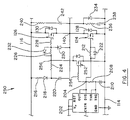
- an oscillator (202) operates at a frequency of 25 KHz and produces an alternating voltage in the form of a square wave which appears at a node (204).
- Oscillator (202) includes a CMOS RC timer which is a self-contained chip of the type identified as an ICM 7555 available from Intersil, Inc. of Cupertino, California, U.S.A.
- capacitor (206) provides a soft start for oscillator (202) which permits capacitor (152) to gradually charge from zero volts to the peak level of, for example, 75 volts.
- An RC network including resistor (208) and capacitor (210), is connected to oscillator (202) as illustrated in Figure 3 and establishes the frequency of operation of the oscillator and voltage converter (200).
- transistor (124) is biased off.
- capacitor (220) ceases to charge through transistor (124) whereby the gate of the transistor quickly discharges through a diode (222) into oscillator (202).
- Capacitor (220) then begins to discharge through a closed loop which includes three resistors (224, 226 and 228) and the gate and source electrodes of transistor 126 whereby the transistor is biased on.
- capacitor (220) functions as a tertiary power source in voltage converter (200) to provide the power to turn on transistor (126).
- transistor (124) and the components in the charging path of the capacitor function as a means for facilitating the development of the voltage of the tertiary power source.
- the shut down of transistor (124) in combination with the three resistors (224, 226 and 228) form a means for applying the voltage of the tertiary power source, i.e. capacitor (220), to turn on transistor (126).
- transistor (126) When transistor (126) is turned on, the source and drain electrodes of the transistor are now in a series loop with capacitor (152) and primary winding (132) whereby the capacitor discharges within the loop to supply current in the second or discharging direction through the primary winding.
- Zener diode (230) is designed to clamp the gate voltage at the saturation voltage level of transistor 126 and thereby prevents any potentially harmful application of voltage to the transistor above the operating voltage level.
- transistor (124) is biased on and transistor (126) is biased off whereby the gate capacitance of transistor (126) discharges quickly through a loop which includes a diode (232), the source and drain electrodes of transistor (124), a diode (234) and resistor (228).
- capacitor (152) functions as a secondary power source and, as noted above, capacitor (220) functions as a tertiary power source. Further, the operation of transistor (124) in conjunction with the circuit for charging capacitor (220) provides a means for establishing the voltage of the tertiary power source.
- a resistor (236) and a capacitor (238) are connected in parallel with the source and drain electrodes of transistor (124) and function as a snubber circuit to provide a bypass around the transistor for any spurious voltage spikes which may occur and which could possibly damage the transistor.
- a resistor (240) and a capacitor (242) are connected in parallel with the source and drain electrodes of transistor (126) and function as a snubber circuit for the transistor.
- FIG 4 there is a partial illustration of voltage converter (250) which is a variation of voltage converter (200) ( Figure 3). Those portions of converter (250) which are not illustrated are identical to corresponding portions of converter (200). In converter (250), diodes (214 and 234) have been removed. Also, transistor (124) has been connected so that the source and drain electrodes thereof are connected between node (140) and line (114) in the same manner as illustrated in Figure 1. Also, the gate of a third N-channel power MOSFET transistor (252) is connected through a resistor (254) to node (204). The source and drain electrodes of transistor (252) are connected between a node (256) and line (114).
- Voltage converter (250) operates in somewhat the same manner as converter (200) ( Figure 3) except that when transistor (124) is biased into conduction, transistor (252) is also biased into conduction. In this manner, transistor (126) is biased off by virtue of the gate thereof being grounded through the source and drain electrodes of transistor (252). Transistor (124) functions as described with respect to converter (200) but without the necessity for diodes (214) ( Figure 3) and (234). Further, capacitor (220) charges through the source and drain electrodes of transistor (124). When transistors (124 and 252) are biased off through control of the output of oscillator (202), capacitor (220) begins to discharge as previously described to turn on transistor (126).
- sensing and control circuit (154) of voltage converter (300) includes a voltage divider network which is formed by a resistor (302) and a rheostat (304) connected in series between lines (114 and 136).
- the resistance values of resistor (302) and rheostat (304) are high, for example 75K ohms and 50K ohms, respectively, and develop voltage levels in response to the ripple voltage of capacitor (152).
- resistor (302) and rheostat (304) form a means for sensing the voltage swing of capacitor (152).
- the voltage developed across rheostat (304) is representative at any instant of the voltage of capacitor (152) and is applied through a tap line (306) to the TRIGGER input of a CMOS RC timer which is connected to function as a one-shot multivibrator (308).
- the CMOS RC timer is a self-contained chip of the type identified as an ICM 7555 available from Intersil, Inc. of Cupertino, California, U.S.A.
- Zener diode (125) is connected to facilitate the application of operating voltage to multivibrator (308) while the OUTPUT terminal is connected to a base (310) of a bipolar transistor (312).
- a resistor (314) and a capacitor (316) are connected in series between the OUTPUT of multivibrator (308) and line (114) while the THRESHOLD and DISCHARGE terminals of the multivibrator are connected to a juncture between the resistor and the capacitor.
- RESET and CONTROL VOLTAGE terminals of oscillator (202) are connected to collector (318) of transistor (312) and to line (114) through soft-start capacitor (206).
- Emitter (320) of transistor (312) is also connected to line (114).
- voltage converter (300) In normal operation, voltage converter (300) is operating properly and there is either no load, or a desired or normal load, connected to output terminals (148 and 150). In either event, the voltage appearing normally across rheostat (304) is greater than one-third the value of the voltage applied to multivibrator (308) between the V+ and GROUND terminals. Under this condition, multivibrator (308) operates in a mode whereby the OUTPUT of the multivibrator is consistently low. This maintains transistor (312) in the non-conductive state. When transistor (312) is not conducting, the RESET terminal of oscillator (202) is high and the oscillator operates constantly at a predetermined periodicity or frequency, for example, of 25 KHz.
- transistors (124 and 126) are controlled to be alternately switched, and thereby operate, at the predetermined frequency of 25 KHz to control current flow through primary winding (132), as described above, and thereby establish the low level D.C. voltage across output terminals (148 and 150).
- multivibrator (308) and transistor (312) form a means for controlling the operation of oscillator (202).
- multivibrator (308) and transistor (312) provide a means, which is responsive to a significant increase in the average voltage level of capacitor (152) resulting from wide swings in the capacitor voltage, for shutting down oscillator (202) and transistors (124 and 126).
- circuit (154) forms a means for sensing voltage swings in the voltage of capacitor (152) and for preventing the operation of either of the transistors (124 or 126) but does not remove power from the other portions of voltage converter (300).
- oscillator (202) develops a square wave output at 25 KHz.
- the square wave output ceases.
- multivibrator (308) operates through an internal timing system within the multivibrator for forty microseconds whereby the OUTPUT of the multivibrator goes low and oscillator (202) again produces the square wave output. If the overload condition is still present, the OUTPUT of multivibrator (308) again goes high resulting in the shut down of oscillator (202). This pattern continues until either the overload condition is corrected or voltage converter (300) is disconnected from A.C. source (112).
- multivibrator (308) functions as a means for periodically examining the load after shutdown of transistors (124 and 126) to determine whether the overload condition persists.
- voltage converter (400) differs from voltage converter (200) ( Figure 3) in the manner in which transistor (126) is controlled to switch on and off in response to the square wave output of oscillator (202).
- a N channel power MOSFET transistor (402) When the output of oscillator (202) is high, a N channel power MOSFET transistor (402) is turned on and, through the drain and source electrodes of the transistor, connects ground reference line (114) to the gate electrode of a N channel power MOSFET transistor (404). This insures that transistor (404) will not turn on and that transistor (126) will not turn on when transistor (124) is on. Also when transistor (124) is turned on, a charging path is formed which includes a diode (406), a capacitor (408) and the source and drain electrodes of the transistor to thereby charge the capacitor essentially to the voltage level appearing between lines (114 and 116).
- capacitor (408) begins to discharge slowly through a path which includes gating resistors (410 and 412), and the gate and source electrodes of transistor (404). The resultant current flow through the gate-source circuit of transistor (404) causes the transistor to turn on.
- Capacitor 408 then begins to discharge more rapidly through a path which includes a parallel combination of a capacitor (414) and a resistor (416), the source and drain electrodes of transistor (408), a pair of current limiting resistors (418 and 420) and the gate and source electrodes of transistor (126).
- Capacitor (414) is a very low-valued capacitor while resistor (416) is of a relatively high resistance value. This permits rapid current flow initially through capacitor (414) until the low-valued capacitor is nearly fully charged whereafter current flows more slowly through resistor (416). The initial rapid current flow through the discharge path of capacitor (408), which includes capacitor 414 and transistor (126), causes the transistor to turn on rapidly.
- a Zener diode (422) is designed to breakdown at the operating voltage level of transistor (126) and thereby prevents any potentially harmful application of voltage to the transistor above the operating voltage level.
- capacitor (408) functions as a tertiary power source of voltage converter (400) and powers the operation of transistor (126).
- transistors (124 and 402) and the components in the charging path of the capacitor function as a means for facilitating the development of the voltage of the tertiary power source.
- the shut down of transistor (402), the turn on of transistor (404) and all of the components associated with the discharge of capacitor 408 form a means for applying the voltage of the tertiary power source, i.e. capacitor (408), to turn on transistor (126).
- Transistor (126) will remain on until transistor (402) is again turned on and the ground reference line (114) is connected thereby to the gate electrode of transistor (404). At this time, capacitor (408) begins to charge as described above and transistor (126) begins to discharge.
- the discharge path for transistor (126) includes resistors (418 and 420), a Zener diode (424) and the source and drain electrodes of now-conducting transistors (124 and 402). Diode (424) insures that the discharging current of transistor (126) will not flow through the gate-source circuit of transistor (404) and thereby prevents potential damage to transistor (404).
- the bias control for the operation of transistor (124) is derived directly through oscillator (202)
- the bias control for the operation of transistor (126) is derived indirectly through oscillator (202) and directly through power buffer (426) which includes a tertiary or separate power source, namely charged capacitor (408).
- Voltage converter (500) is illustrated collectively in Figures 7A and 7B.
- sensing and control circuit (154) senses swings in the voltage of capacitor (152) and controls the on-off operation of oscillator (202) in response thereto. In turn, this determines whether transistors (124 and 126) operate in the alternately switched mode or whether the transistors are shut down completely.
- transistor (402) In the operation of power buffer (426) to bias and control the operation of transistor (126) as previously described, transistor (402) is biased to operate simultaneously with transistor (124). In this manner, transistor (404) is biased off during operation of transistor (124) and the voltage of the tertiary power supply, i.e., capacitor (408), is not applied to transistor (126) whereby transistor (126) is biased off. Therefore, transistor (402) must be conducting in order to maintain transistor (126) in the "off" mode.
- the OUTPUT of multivibrator (308) is connected through a diode (502) ( Figure 7B) to the gate electrode of transistor (402).
- the OUTPUT of oscillator (202) is connected through a diode (504) ( Figure 7B) to the gate electrode of transistor (402).
- transistor (124) is connected to oscillator (202) in the same manner illustrated in Figure 5 and power buffer (426) is connected to transistor (126) as illustrated in Figure 6.
- voltage converter 500 operates in the same manner as voltage converter (400) during the no-load mode or the normal-load mode.
- multivibrator 308 is biased to go high at the OUTPUT in order to shut down oscillator (202).
- the high OUTPUT of multivibrator (308) also is coupled through diode (502) to the gate electrode of transistor (402) to insure that the transistor remains on when oscillator (202) is shut down and thereby insures that transistor (126) remains shut down.
- transistor 402 is biasingly controlled by oscillator (202) during a no-load mode or a normal-load mode and is controlled by multivibrator (308) during an overload mode.
- voltage converters (100, 200, 250, 300, 400 and 500) provide a variety of embodiments which convert high A.C. voltage, or high D.C. voltage, to a low level D.C. voltage.
- These various embodiments employ the basic concept of applying a voltage during alternate periods to high frequency step-down transformer (134) and rectifying the transformer output to obtain the low level D.C. voltage.
- capacitor (152) functions as a power source during one of the alternate periods to apply voltage to transformer (134).
- each of the voltage converters employs techniques for protecting the converter when an overload condition occurs.
- voltage conditions are constantly monitored during circuit operation to determine when an overload occurs and to shut down the converter operation.
- the circuit is monitored during operation and if excessive current flow develops the current is shunted to avoid destruction to components of the converter.
- both of the converter protection techniques are employed.
- voltage converters (100, 200, 250, 300, 400 and 500) operate at high speeds and at high efficiency. Also, comparatively fewer components are required which provides an economic advantage. Significantly, each of the voltage converters (100, 200, 250, 300, 400 and 500) provide simple and effective facility for protecting the converter in the event of an overload.
- converters (100, 200, 250, 300, 400 and 500) are referred to herein as voltage converters, these converters could be referred to, for example, as power converters or any other comparable expression without departing from the spirit and scope of the invention.
- Power buffers such as buffer (600) are typically used for converting DC power to AC power at a desired or prescribed output voltage and frequency. Buffers of this type are also typically used as power supplies for a variety of systems, as variable-speed AC motor drives, for induction heating systems and as an output of DC transmission lines.
- a pair of power field effect transistors are alternately switched to facilitate the supply of current to a load in opposite directions from two alternate DC sources such as alternate batteries.
- the on-off operation of a first of the power transistors is controlled through a first switching bipolar transistor by the application of a square wave pulse to the switching transistor.
- a second of the power transistors is powered by the voltage of a capacitor which is charged from a battery independent of the two alternate batteries of the power buffer.
- a second switching bipolar transistor is also responsive to the square wave pulse to control the operation of a third switching bipolar transistor which facilitates application of the capacitor voltage to the second power transistor.
- the buffer described in the previous paragraph requires two power field effect transistors, three bipolar N-P-N transistors and a third battery to charge the capacitor for operating one of the power transistors.
- Power buffer (600) includes four N channel MOSFET power transistors (602, 604, 606 and 608). Power buffer (600) further includes power output terminals (610, 612 and 614). The positive side of a first DC supply battery (616) is connected through terminal (610) to the drain electrode of transistor (602). The negative side of a second DC supply battery (618) is connected through terminal (614) to the source electrode of transistor (604). The other side of each of the batteries (616 and 618) is connected to one side of a load, the other side of which is connected to terminal (612).
- Power buffer (600) further includes a pair of input terminals (620 and 622) which provide binary signal inputs to the buffer to control the operation thereof. As illustrated in Figure 8, a binary generator (624) is coupled to power buffer (600) through input terminals (620 and 622) to control the operation of transistor (602 and 604).
- transistor (604) Assume initially that through control of binary generator (624), the input terminals (620 and 622) are both high.
- the gate electrode of transistor (604) is connected to terminal (620) through a low-valued resistor (626).
- a reverse biased diode (628) is connected in parallel with resistor (626).
- transistor (604) When transistor (604) is turned on, a charging path is formed which includes a diode (632), a capacitor (634) and the source and drain electrodes of the transistor to thereby charge the capacitor essentially to the cumulative voltage level of batteries (616 and 618). Also, when transistor (604) is on, the load is connected in a series circuit which includes battery (618) and the source and drain electrodes of the transistor whereby current is supplied to the load in a first direction.
- transistor (606) When terminal (622) is high, as noted above, transistor (606) is turned on. Through the drain and source electrodes of transistor (606), the negative side of battery 618 is connected to the gate electrode of transistor (608) to prevent transistor (608) from turning on. This insures that transistor (602) will not turn on at this time.
- terminals (620 and 622) go low whereby transistors (604 and 606) are turned off.
- transistor (606) is turned off, the gate electrode of transistor (608) is disconnected from the negative side of battery (618).
- the charging path for capacitor (634) is now open and the capacitor is precluded from discharging through the charging path by the inverse connection of diode (632).
- capacitor (634) begins to discharge slowly through a path which includes gating resistors (636 and 638), and the gate and source electrodes of transistor (608).
- the resultant current flow through the gate-source circuit of transistor (608) causes the transistor to turn on.
- Capacitor (634) then begins to discharge more rapidly through a path which includes a parallel combination of a capacitor (640) and a resistor (642), the source and drain electrodes of transistor (608), a pair of current limiting resistors (644 and 646) and the gate and source electrodes of transistor (602).
- Capacitor (640) is a very low-valued capacitor while resistor (642) is of a relatively high resistance value. This permits rapid current flow initially through capacitor (640) until the low-valued capacitor is nearly fully charged whereafter current flows more slowly through resistor (642). The initial rapid current flow through the discharge path of capacitor (634), which includes capacitor 640 and transistor (602), causes the transistor to turn on rapidly.
- a Zener diode (648) is designed to breakdown at the operating voltage level of transistor (602) and thereby prevents any potentially harmful application of voltage to the transistor above the operating voltage level.
- Transistor (602) will remain on until transistor (606) is again turned on and the negative side of battery (618) is connected to the gate electrode of transistor (608). At this time, capacitor (634) begins to charge as described above and transistor (602) begins to discharge.
- the discharge path for transistor (602) includes resistors (644 and 646), a Zener diode (650) and the source and drain electrodes of transistors (604 and 606). Diode (650) insures that the discharging current of transistor (602) will not flow through the gate-source circuit of transistor (608) and thereby prevents potential damage to transistor (608).
- terminals (620) and (622) were either both high or both low to provide an alternating current through the load. This was accomplished by alternately switching power transistors (602 and 604) by control of the binary inputs to power buffer (600).
- the binary generator (624) can be controlled so that terminal (620) is low and terminal (622) is high. In this manner, both transistors (602 and 604) will be shut down.
- transistor (604) is conducting and the gate of transistor (602) is biased on due to spurious noise in the electrical systems, the gate charge will dissipate through transistor (606) thereby forcing transistor (602) to turn off. Also, this eliminates a need for special logic to produce a delay between turn on and turn off of transistors (602 and 604).
- Power buffer (600) provides a circuit which is simple and which utilizes only fast-acting voltage-sensitive power transistors. Further, in power buffer (600), the voltage of supply batteries (616 and 618) establishes another DC supply voltage source by charging capacitor (634). The established DC supply voltage source of capacitor (640) then, upon demand, provides the necessary voltage to turn on transistor (602) as described. Consequently, there is no need for an additional battery to charge capacitor (634).
Landscapes
- Engineering & Computer Science (AREA)
- Power Engineering (AREA)
- Dc-Dc Converters (AREA)
Applications Claiming Priority (3)
| Application Number | Priority Date | Filing Date | Title |
|---|---|---|---|
| US07/161,122 US4945467A (en) | 1988-02-26 | 1988-02-26 | Multiple-mode voltage converter |
| US161122 | 1988-02-26 | ||
| EP89903305A EP0402395A1 (fr) | 1988-02-26 | 1989-02-23 | Transformateur de tension |
Related Parent Applications (1)
| Application Number | Title | Priority Date | Filing Date |
|---|---|---|---|
| EP89903305.4 Division | 1989-02-23 |
Publications (2)
| Publication Number | Publication Date |
|---|---|
| EP0600522A2 true EP0600522A2 (fr) | 1994-06-08 |
| EP0600522A3 EP0600522A3 (fr) | 1994-12-07 |
Family
ID=22579912
Family Applications (2)
| Application Number | Title | Priority Date | Filing Date |
|---|---|---|---|
| EP89903305A Ceased EP0402395A1 (fr) | 1988-02-26 | 1989-02-23 | Transformateur de tension |
| EP19930119915 Withdrawn EP0600522A3 (fr) | 1988-02-26 | 1989-02-23 | Convertisseur de tension avec circuit intermédiaire à haute fréquence. |
Family Applications Before (1)
| Application Number | Title | Priority Date | Filing Date |
|---|---|---|---|
| EP89903305A Ceased EP0402395A1 (fr) | 1988-02-26 | 1989-02-23 | Transformateur de tension |
Country Status (6)
| Country | Link |
|---|---|
| US (1) | US4945467A (fr) |
| EP (2) | EP0402395A1 (fr) |
| JP (1) | JPH03503954A (fr) |
| AU (1) | AU629490B2 (fr) |
| CA (1) | CA1297533C (fr) |
| WO (1) | WO1989008347A1 (fr) |
Cited By (1)
| Publication number | Priority date | Publication date | Assignee | Title |
|---|---|---|---|---|
| CN109739107A (zh) * | 2018-12-18 | 2019-05-10 | 西北工业大学 | 一种基于模型预测控制的功率缓冲器设计方法 |
Families Citing this family (14)
| Publication number | Priority date | Publication date | Assignee | Title |
|---|---|---|---|---|
| US5291382A (en) * | 1991-04-10 | 1994-03-01 | Lambda Electronics Inc. | Pulse width modulated DC/DC converter with reduced ripple current coponent stress and zero voltage switching capability |
| US5303137A (en) * | 1991-12-04 | 1994-04-12 | Dawn Technologies, Ltd. | Multiresonant self-oscillating converter circuit |
| US5528484A (en) * | 1993-01-14 | 1996-06-18 | H.P.M. Industries Pty Limited | Power supply |
| US5303138A (en) * | 1993-04-29 | 1994-04-12 | At&T Bell Laboratories | Low loss synchronous rectifier for application to clamped-mode power converters |
| US5455496A (en) * | 1993-05-14 | 1995-10-03 | Siliconix Incorporated | Head-retract circuit for moving media storage apparatus |
| US5508874A (en) * | 1993-05-14 | 1996-04-16 | Siliconix Incorporated | Disconnect switch circuit to power head retract in hard disk drive memories |
| US5459654A (en) * | 1993-05-14 | 1995-10-17 | Siliconix Incorporated | Apparatus for generating positive and negative supply rails from operating motor control circuit |
| AU686668B2 (en) * | 1993-11-12 | 1998-02-12 | Johan Christiaan Fitter | A power converter |
| US5590032A (en) | 1995-05-25 | 1996-12-31 | Lucent Technologies Inc. | Self-synchronized drive circuit for a synchronous rectifier in a clamped-mode power converter |
| US5864472A (en) * | 1997-03-24 | 1999-01-26 | Ault Incorporated | Apparatus for controlling a multiresonant self-oscillating converter circuit |
| TW434991B (en) | 1997-09-26 | 2001-05-16 | Hitachi Koki Kk | DC power source unit alarming before electrically powered tool is overheated and stopping power supply thereafter |
| US6495932B1 (en) | 1997-09-26 | 2002-12-17 | Hitachi Koki Co., Ltd. | DC power source unit |
| WO2010010418A1 (fr) * | 2008-07-25 | 2010-01-28 | Osram Gesellschaft mit beschränkter Haftung | Convertisseur à résonance ayant une meilleure protection contre les surcharges et procédé correspondant |
| US9285865B2 (en) * | 2012-06-29 | 2016-03-15 | Oracle International Corporation | Dynamic link scaling based on bandwidth utilization |
Family Cites Families (45)
| Publication number | Priority date | Publication date | Assignee | Title |
|---|---|---|---|---|
| US3257604A (en) * | 1961-07-07 | 1966-06-21 | Westinghouse Electric Corp | Inverter |
| US3315144A (en) * | 1963-10-18 | 1967-04-18 | Electronic Energy Conversion C | Capacitor charge reversing circuit |
| US3596165A (en) * | 1969-07-24 | 1971-07-27 | Tektronix Inc | Converter circuit having a controlled output |
| FR2205763B1 (fr) * | 1972-11-02 | 1976-11-19 | Siemens Ag | |
| US3925633A (en) * | 1974-09-06 | 1975-12-09 | Donald F Partridge | Circuit for controlling power flow from a high frequency energy source to a plurality of high frequency loads |
| US4005370A (en) * | 1974-09-10 | 1977-01-25 | Matsushita Electric Industrial Co., Ltd. | Power supply means for magnetron |
| US4017784A (en) * | 1976-05-17 | 1977-04-12 | Litton Systems, Inc. | DC to DC converter |
| AT345389B (de) * | 1976-06-01 | 1978-09-11 | Siemens Ag Albis | Spannungs- oder stromgeregelter spannungswandler |
| US4167776A (en) * | 1976-07-19 | 1979-09-11 | Danfoss A/S | Inverter circuit |
| US4122514A (en) * | 1976-11-01 | 1978-10-24 | Hewlett-Packard Company | Direct current power supply |
| US4092711A (en) * | 1976-12-29 | 1978-05-30 | Honeywell Information Systems Inc. | Power supply with automatic shutdown |
| US4055790A (en) * | 1976-12-29 | 1977-10-25 | Honeywell Information Systems Inc. | Power supply with base drive control |
| GB1602613A (en) * | 1977-06-24 | 1981-11-11 | Chloride Group Ltd | Converters |
| US4126819A (en) * | 1977-07-01 | 1978-11-21 | Kearney & Trecker Corporation | Interlock circuit for complementary electronic switches |
| US4201957A (en) * | 1977-09-21 | 1980-05-06 | Qualidyne Systems, Inc. | Power inverter having parallel switching elements |
| US4178628A (en) * | 1978-05-12 | 1979-12-11 | R & I Patent Corporation | Switching type regulated power supply |
| NL7809226A (nl) * | 1978-09-11 | 1980-03-13 | Philips Nv | Geschakelde spanningsomzetter. |
| GB2043370B (en) * | 1979-02-28 | 1983-03-09 | Chloride Group Ltd | Converters |
| US4310866A (en) * | 1979-09-28 | 1982-01-12 | Borg-Warner Corporation | Shootthrough fault protection system for bipolar transistors in a voltage source transistor inverter |
| US4316243A (en) * | 1979-12-17 | 1982-02-16 | General Electric Company | Power FET inverter drive circuit |
| GB2086672B (en) * | 1980-10-31 | 1985-03-13 | Jones Walter & Co Engineers Lt | Single phase inverter |
| US4347558A (en) * | 1981-04-02 | 1982-08-31 | Rockwell International Corporation | Voltage balance control for split capacitors in half bridge DC to DC converter |
| JPS57193819A (en) * | 1981-04-28 | 1982-11-29 | Toko Inc | Switching regulator |
| US4408270A (en) * | 1981-07-16 | 1983-10-04 | General Electric Company | Stored charge inverter circuit with rapid switching |
| NZ201203A (en) * | 1981-07-28 | 1985-08-30 | Lee Electric Lighting | Arc lamp supply:fet bridge inverter powered by constant current source |
| DE3138645A1 (de) * | 1981-09-29 | 1983-04-14 | Dr.Ing.H.C. F. Porsche Ag, 7000 Stuttgart | "elektronische ueberstromschutzvorrichtung" |
| JPS5878386A (ja) * | 1981-11-04 | 1983-05-11 | 松下電器産業株式会社 | 誘導加熱用インバ−タ装置 |
| US4383293A (en) * | 1981-11-16 | 1983-05-10 | Acme Electric Corporation | Isolated DC current sense circuit |
| SE429220B (sv) * | 1981-12-17 | 1983-08-22 | Bengt J Sterner | Av oberoende av varandra alstrade pulsfoljder styrd elektrisk sekerhetsanordning |
| US4429359A (en) * | 1981-12-24 | 1984-01-31 | General Electric Company | Inverter circuit with symmetry control |
| US4464709A (en) * | 1982-04-06 | 1984-08-07 | Tektronix, Inc. | Current and voltage protection for a power supply circuit |
| US4404623A (en) * | 1982-04-23 | 1983-09-13 | Florida Computer Graphics | Method and apparatus for balancing flux in a power transformer circuit |
| US4455545A (en) * | 1982-11-05 | 1984-06-19 | Sperry Corporation | High frequency output inductor for inverter power supply |
| JPS59128128A (ja) * | 1983-01-13 | 1984-07-24 | Matsushita Electric Works Ltd | 積載方法 |
| DE3305224A1 (de) * | 1983-02-16 | 1984-08-16 | Bbc Brown Boveri & Cie | Bord-batterieladegeraet |
| US4594650A (en) * | 1983-04-19 | 1986-06-10 | Mitsubishi Denki Kabushiki Kaisha | Inverter device |
| US4535399A (en) * | 1983-06-03 | 1985-08-13 | National Semiconductor Corporation | Regulated switched power circuit with resonant load |
| GB2142495B (en) * | 1983-06-24 | 1986-09-17 | Barry Wayne Williams | Switch-off circuits for transistors and gate turn-off thyristors |
| US4533986A (en) * | 1983-10-31 | 1985-08-06 | General Electric Company | Compact electrical power supply for signal processing applications |
| US4550359A (en) * | 1984-02-10 | 1985-10-29 | Honeywell Inc. | Voltage transient protection circuit for MOSFET power transistors |
| US4631653A (en) * | 1984-05-25 | 1986-12-23 | Boschert Incorporated | Capacitor coupled current mode balance circuit |
| US4564800A (en) * | 1984-06-01 | 1986-01-14 | Jetronic Industries, Inc. | Battery charger |
| US4586118A (en) * | 1984-06-05 | 1986-04-29 | The United States Of America As Represented By The United States Department Of Energy | Capacitor charging FET switcher with controller to adjust pulse width |
| GB2170663B (en) * | 1985-02-02 | 1989-06-14 | Brian Ernest Attwood | Harmonic-resonant power supply |
| US4719559A (en) * | 1986-10-22 | 1988-01-12 | Cherry Semiconductor Corporation | Current-mode control of capacitively coupled power converters |
-
1988
- 1988-02-26 US US07/161,122 patent/US4945467A/en not_active Expired - Fee Related
-
1989
- 1989-02-10 CA CA000590690A patent/CA1297533C/fr not_active Expired - Lifetime
- 1989-02-23 WO PCT/US1989/000729 patent/WO1989008347A1/fr not_active Ceased
- 1989-02-23 EP EP89903305A patent/EP0402395A1/fr not_active Ceased
- 1989-02-23 JP JP1503116A patent/JPH03503954A/ja active Pending
- 1989-02-23 EP EP19930119915 patent/EP0600522A3/fr not_active Withdrawn
- 1989-02-23 AU AU33486/89A patent/AU629490B2/en not_active Ceased
Cited By (2)
| Publication number | Priority date | Publication date | Assignee | Title |
|---|---|---|---|---|
| CN109739107A (zh) * | 2018-12-18 | 2019-05-10 | 西北工业大学 | 一种基于模型预测控制的功率缓冲器设计方法 |
| CN109739107B (zh) * | 2018-12-18 | 2022-03-18 | 西北工业大学 | 一种基于模型预测控制的功率缓冲器设计方法 |
Also Published As
| Publication number | Publication date |
|---|---|
| US4945467A (en) | 1990-07-31 |
| EP0402395A1 (fr) | 1990-12-19 |
| WO1989008347A1 (fr) | 1989-09-08 |
| AU629490B2 (en) | 1992-10-01 |
| AU3348689A (en) | 1989-09-22 |
| CA1297533C (fr) | 1992-03-17 |
| JPH03503954A (ja) | 1991-08-29 |
| EP0600522A3 (fr) | 1994-12-07 |
Similar Documents
| Publication | Publication Date | Title |
|---|---|---|
| US4945467A (en) | Multiple-mode voltage converter | |
| US4691270A (en) | Current fed inverter bridge with lossless snubbers | |
| US4709316A (en) | Single-ended DC-to-DC converter with lossless switching | |
| JP2636918B2 (ja) | 疑似共振電流モード静止電力変換方法及び装置 | |
| JP3459142B2 (ja) | 駆動パルス出力制限回路 | |
| KR100541724B1 (ko) | 모터전원공급장치 및 모터전원공급방법 | |
| US3913002A (en) | Power circuits for obtaining a high power factor electronically | |
| JPS61112583A (ja) | 電力変換装置 | |
| US6256209B1 (en) | AC to DC conversion arrangement | |
| US5657212A (en) | Capacitor coupled converter | |
| US5303137A (en) | Multiresonant self-oscillating converter circuit | |
| EP0125278B1 (fr) | Alimentation ayant une source de courant continu d'entree et des etages d'alimentation a courant pulse | |
| US5864472A (en) | Apparatus for controlling a multiresonant self-oscillating converter circuit | |
| JPH07284266A (ja) | ゲート充電フィルタを有する電源方法及び装置 | |
| CN111130376B (zh) | 三相脉宽调制整流电路及其预充电方法 | |
| WO1994014230A1 (fr) | Convertisseur auto-oscillant a inductance serie comprenant une bobine d'inductance oscillante en trois parties | |
| EP0212817B1 (fr) | Onduleurs | |
| JP3335639B2 (ja) | シリコン制御整流器フルブリッジ回路を有するインバータ | |
| RU2109394C1 (ru) | Квазирезонансный преобразователь постоянного напряжения с переключением при нулевом напряжении | |
| JP2673996B2 (ja) | インバータ装置 | |
| SU1365300A1 (ru) | Преобразователь переменного напр жени в посто нное | |
| JPH0270267A (ja) | 並列形共振コンバータ | |
| SU1654956A1 (ru) | Преобразователь посто нного напр жени | |
| JPH0626470B2 (ja) | スイッチング回路 | |
| JPH06311755A (ja) | インバータ装置 |
Legal Events
| Date | Code | Title | Description |
|---|---|---|---|
| PUAI | Public reference made under article 153(3) epc to a published international application that has entered the european phase |
Free format text: ORIGINAL CODE: 0009012 |
|
| AC | Divisional application: reference to earlier application |
Ref document number: 402395 Country of ref document: EP |
|
| AK | Designated contracting states |
Kind code of ref document: A2 Designated state(s): DE FR GB IT |
|
| PUAL | Search report despatched |
Free format text: ORIGINAL CODE: 0009013 |
|
| AK | Designated contracting states |
Kind code of ref document: A3 Designated state(s): DE FR GB IT |
|
| 17P | Request for examination filed |
Effective date: 19950209 |
|
| 17Q | First examination report despatched |
Effective date: 19950919 |
|
| STAA | Information on the status of an ep patent application or granted ep patent |
Free format text: STATUS: THE APPLICATION IS DEEMED TO BE WITHDRAWN |
|
| 18D | Application deemed to be withdrawn |
Effective date: 19960330 |