EP0599414A2 - Direktumsetzempfänger - Google Patents
Direktumsetzempfänger Download PDFInfo
- Publication number
- EP0599414A2 EP0599414A2 EP93203239A EP93203239A EP0599414A2 EP 0599414 A2 EP0599414 A2 EP 0599414A2 EP 93203239 A EP93203239 A EP 93203239A EP 93203239 A EP93203239 A EP 93203239A EP 0599414 A2 EP0599414 A2 EP 0599414A2
- Authority
- EP
- European Patent Office
- Prior art keywords
- arrangement
- frequency
- signal
- direct conversion
- quadrature
- Prior art date
- Legal status (The legal status is an assumption and is not a legal conclusion. Google has not performed a legal analysis and makes no representation as to the accuracy of the status listed.)
- Granted
Links
- 238000006243 chemical reaction Methods 0.000 title claims abstract description 38
- 238000012935 Averaging Methods 0.000 claims abstract description 5
- 230000010363 phase shift Effects 0.000 claims description 17
- 238000001514 detection method Methods 0.000 abstract description 10
- 230000004044 response Effects 0.000 abstract description 6
- 239000013078 crystal Substances 0.000 description 6
- 230000000694 effects Effects 0.000 description 5
- 230000006870 function Effects 0.000 description 5
- 239000003990 capacitor Substances 0.000 description 3
- 238000001914 filtration Methods 0.000 description 3
- 238000009499 grossing Methods 0.000 description 3
- 238000005259 measurement Methods 0.000 description 3
- 230000009467 reduction Effects 0.000 description 3
- 230000003595 spectral effect Effects 0.000 description 3
- 238000013459 approach Methods 0.000 description 2
- 230000005540 biological transmission Effects 0.000 description 2
- 125000004122 cyclic group Chemical group 0.000 description 2
- 230000003111 delayed effect Effects 0.000 description 2
- 238000001228 spectrum Methods 0.000 description 2
- 230000009471 action Effects 0.000 description 1
- 230000032683 aging Effects 0.000 description 1
- 230000009118 appropriate response Effects 0.000 description 1
- 230000008901 benefit Effects 0.000 description 1
- 230000008859 change Effects 0.000 description 1
- 238000010168 coupling process Methods 0.000 description 1
- 238000005859 coupling reaction Methods 0.000 description 1
- 230000001934 delay Effects 0.000 description 1
- 230000003287 optical effect Effects 0.000 description 1
- 230000000007 visual effect Effects 0.000 description 1
Images


Classifications
-
- H—ELECTRICITY
- H04—ELECTRIC COMMUNICATION TECHNIQUE
- H04B—TRANSMISSION
- H04B1/00—Details of transmission systems, not covered by a single one of groups H04B3/00 - H04B13/00; Details of transmission systems not characterised by the medium used for transmission
- H04B1/06—Receivers
- H04B1/16—Circuits
- H04B1/30—Circuits for homodyne or synchrodyne receivers
-
- H—ELECTRICITY
- H03—ELECTRONIC CIRCUITRY
- H03J—TUNING RESONANT CIRCUITS; SELECTING RESONANT CIRCUITS
- H03J7/00—Automatic frequency control; Automatic scanning over a band of frequencies
- H03J7/02—Automatic frequency control
-
- H—ELECTRICITY
- H03—ELECTRONIC CIRCUITRY
- H03D—DEMODULATION OR TRANSFERENCE OF MODULATION FROM ONE CARRIER TO ANOTHER
- H03D3/00—Demodulation of angle-, frequency- or phase- modulated oscillations
- H03D3/007—Demodulation of angle-, frequency- or phase- modulated oscillations by converting the oscillations into two quadrature related signals
-
- H—ELECTRICITY
- H03—ELECTRONIC CIRCUITRY
- H03D—DEMODULATION OR TRANSFERENCE OF MODULATION FROM ONE CARRIER TO ANOTHER
- H03D7/00—Transference of modulation from one carrier to another, e.g. frequency-changing
- H03D7/16—Multiple-frequency-changing
- H03D7/165—Multiple-frequency-changing at least two frequency changers being located in different paths, e.g. in two paths with carriers in quadrature
Definitions
- the present invention relates to a direct conversion receiver comprising a local frequency generating arrangement which is coupled to a pair of quadrature related mixers for mixing down an rf input signal to quadrature related signals, and a.f.c. means for providing a control signal for the local frequency generating arrangement, the a.f.c. means, which are coupled to quadrature paths, comprising an offset frequency detector for determining a signal as the control signal, of which an average value is proportional to a frequency offset of the local frequency generating arrangement with respect to the rf input signal, whereby the offset frequency detector comprises a series arrangement of a phase shifting arrangement and a multiplication arrangement in a quadrature path.
- Such direct conversion receivers can be digital paging receivers or transceivers using an FSK (Frequency Shift Keying) modulation scheme, but also transceivers for cordless telephony or the like.
- a direct conversion receiver of this kind is known from the European Patent EP 298 484 B1.
- an a.f.c. (automatic frequency control) signal for a local oscillator with inherent correct polarity is derived from so-called I- and Q-channel receiver paths.
- a baseband I-channel signal is fed to an offset frequency detector, together with a quadrature related Q-channel signal.
- the offset frequency detector is a series arrangement of a phase shifting arrangement and a multiplication arrangement, whereby the I-channel signal is fed to an input of the multiplication arrangement, and the Q-channel signal is fed to another input of the multiplication arrangement via the phase shifting arrangement.
- An output signal of the offset frequency detector is fed to the local oscillator via a low pass filter.
- the control signal is a bipolar signal, which is subject to a relatively strong low frequency ripple component.
- a direct conversion receiver is characterised in that the frequency detector comprises another series arrangement of a phase shifting arrangement and a multiplication arrangement in another quadrature path, and a subtracting arrangement for subtracting output signals of the multiplication arrangements, whereby inputs of the multiplication arrangements are cross-coupled to the quadrature paths, and other inputs of the multiplication arrangements, are coupled to the quadrature paths via the phase shifting arrangements.
- the control signal comprises a considerable higher ripple frequency component as compared with the known receiver, thus a successive low pass filter for filtering of the control signal can have a much higher cut-off frequency, so that the a.f.c. loop has got a quicker response. This is advantageous for a quick frequency lock and also for scanning frequency channels.
- the filter cut-off frequency should not become too low with respect to the ripple frequency of the control signal, i.e. a trade-off has to be made between a fast loop response and a clean a.f.c. signal.
- a direct conversion receiver according to the present invention e.g. as an FSK data paging receiver for high frequencies such as in the 900 MHz band
- use of expensive temperature compensating schemes for compensating frequency drift of a crystal oscillator in such a receiver as is necessary in conventional paging receivers is also avoided.
- phase shifting arrangement and the multiplication arrangement can be implemented by using analog circuits, in a simple embodiment the phase shifting arrangement is a shift register and the multiplication arrangement is an exclusive-OR. In such an embodiment, the phase shifting arrangement has a phase shift proportional to frequency, i.e. is a time delay arrangement.
- An alternative embodiment of a direct conversion receiver according to the present invention comprises a microcontroller functionally implementing the series arrangements and the subtracting arrangement, and digital-to-analog conversion means and/or digital output means for providing the control signal.
- the direct conversion receiver comprises a microcontroller with digital I/O-channels and/or a digital-to-analog converter for other purposes, and such resources can be shared for implementing the present invention. The shared resources can be multiplexed, then.
- control signal is fed to the local oscillator via an analog or digital integrator or via an analog or digital low pass filter.
- the a.f.c. loop dynamics can be easily controlled.
- Using an integrator achieves a zero steady state response.
- the digital embodiment is particularly advantageous if microcontroller resources can be shared, as mentioned above.
- the direct conversion receiver comprises a data demodulation arrangement in parallel with the offset frequency detector for providing data from the quadrature related baseband signals, a data filter for providing filtered data, and an out-of-range decision arrangement coupled to the data filter via an averaging filter, whereby the decision arrangement controls a switching arrangement for switching an output signal of the offset frequency detector as the control signal, or the filtered data as the control signal.
- a range extension e.g. in an FSK receiver, is necessary if the frequency of the local oscillator drifts close to or beyond the frequency deviation of the received r.f. FSK data signal.
- the out-of-range decision arrangement which can be a window comparison arrangement, detects such an out-of-range condition, and the filtered data is taken as an a.f.c. control signal instead of an output signal of the offset frequency detector.
- Such an out-of-range detection is particularly effective if the number of ones and zeroes in the FSK signal is approximately equal, on the average.
- the out-of-range detection can also be a software-based decision arrangement implemented with a microcontroller, which checks data validity or other signal parameters like signal frequency for taking an out-of-range decision. In case of checking signal frequencies, checking a frequency of a product signal of the I and Q channels, i.e. checking a double frequency, more accurate measurement is achieved than checking the frequency of an I or Q channel alone. Checking data validity can be based on a valid CRC (Cyclic Redundancy Code), a BER (Bit Error Rate), or the like.
- An embodiment of a direct conversion device comprises bandpass filters in the respective quadrature paths, wherein for a.f.c. out-of-range extension the bandpass filters are stopband filters stopping a band substantially from DC, or wherein for out-of-range extension the direct conversion receiver comprises highpass filters coupled to the quadrature paths, whereby the combined bandpass and highpass filters form stopband filters, and wherein the phase shifting arrangements have a non-linear shifting characteristic approaching a predetermined phase shift with increasing frequency.
- the stopband or frequency gap is chosen such that for a zero offset frequency, the received signal frequency just falls outside the gap, whereas for an offset beyond the frequency deviation of the input rf signal one of the FSK data "0" and "1" frequencies falls inside the gap. It is thus achieved that the gap suppresses a signal that would otherwise pull the a.f.c. into the wrong direction.
- An embodiment of a direct conversion device comprises filters in the respective quadrature paths, wherein for a.f.c. out-of-range extension the phase shifting arrangements have a non-linear phase shifting characteristic changing from a first predetermined phase shift to a second predetermined phase shift with increasing baseband frequency around a predetermined baseband frequency (which could also be ⁇ f, ⁇ f being a frequency deviation).
- a predetermined baseband frequency which could also be ⁇ f, ⁇ f being a frequency deviation.
- FIG. 1 schematically shows a direct conversion receiver 1 according to the present invention.
- the direct conversion receiver 1 which can be a paging transceiver, comprises an antenna 2 for receiving an rf (radio frequency) input signal rf, which can be an rf FSK (Frequency Shift Keying) signal carrying FSK modulated digital signals.
- the rf input signal rf is fed to a low noise rf amplifier 3, which is coupled to quadrature paths 4 and 5, so-called I- and Q-channels, for mixing down the rf input signal rf to quadrature related baseband signals I and Q.
- the quadrature path 4 comprises a phase shifting device 6 causing a +45 degrees phase shift of the amplified rf signal.
- the phase shifting device 6 is coupled to a mixer 7 for mixing down the rf signal rf to the baseband signal I, an output of the mixer 7 being filtered and limited by means of a respective filter 8 and a limiter 9.
- the quadrature path 5 comprises a phase shifting device 10 causing a -45 degrees phase shift of the amplified rf signal, a mixer 11, a filter 12, and a limiter 13 for achieving the baseband signal Q.
- the filters 8 and 12 are provided for limiting the noise bandwidth and for channel selectivity. By AC-coupling of the filters 8 and 12 to the mixers 7 and 11, DC-offset effects are avoided.
- the limiters 9 and 13 are provided for removing amplitude signal variations.
- the mixers 7 and 11 are further coupled to a local frequency generating arrangement, e.g. a crystal oscillator having a crystal 15 as a frequency determining element, via a frequency multiplication arrangement 16.
- the local frequency generating arrangement 14 can also be a more elaborate arrangement, e.g. a frequency synthesizer having a crystal oscillator for providing a reference frequency.
- Such frequency synthesizers can operate on the basis of a PLL (Phase Locked Loop).
- the mixing frequency i.e. an output frequency f L of the multiplication arrangement 16, further denoted as oscillator frequency, is chosen such that baseband zero-intermediate frequency signals I and Q are obtained, for a fictitious carrier f C .
- a single 90 degrees phase shifting device can be applied, for phase shifting the oscillator signal for one of mixer signals.
- a frequency offset of the oscillator frequency f L with respect to the rf input signal rf i.e.
- the direct conversion receiver 1 comprises a.f.c. means coupled to the quadrature paths 4 and 5 comprising an offset frequency detector 17 for determining a signal dct as an a.f.c. control signal for the local oscillator 14, a DC (Direct Current) component of the signal dct being proportional to the frequency offset f L -f C , the offset frequency detector 17 compsing two series arrangements of a phase shifting arrangement and a multiplication arrangement and a subtracting or adding arrangement, to be described in detail in connection with figure 2.
- the signal dct practically is fed to the local oscillator 14 via a smoothing arrangement 18, being an analog or digital integrator, or an analog or digital low pass filter, i.e. an actual control signal ct is the smoothed signal dct.
- the signal dct can be an analog or digital signal, depending whether or not the quadrature paths comprise limiters. Poles and zeroes of the smoothing arrangement 18 or smoothing filter determine a.f.c. loop dynamics.
- a filter cut-off frequency could be in a range between a ripple frequency of the digital signal dct divided by 1000 and a frequency of the digital signal dct divided by 20, a trade-off being made between a noisy, but fast loop, and a slower, but more stable loop.
- a fast loop response is required for fast channel scanning or for fast locking.
- a higher ripple frequency allows for a better overall performance.
- the present invention achieves an a.f.c. control signal with an inherent correct polarity, obviating the need for multiplication with demodulated data, such as in other prior art receivers, e.g. as disclosed in GB 2 180 419.
- the direct conversion receiver 1 comprises a demodulator 19 to which the baseband signals I and Q are fed.
- the demodulator 19 can be a lead-lag phase detector for demodulating FSK data.
- the demodulator is coupled to a microcontroller 20 with RAM and ROM memory and digital and/or analog I/O-interfaces.
- microcontrollers are well known in the art.
- various output signals may be provided for such as a speech signal via an amplifier 21 and a speech reproducing device 22, an information message via a display unit 23, a audible tone signal via a bleeper 24, and a visual alert signal via an LED 25.
- a paging transceiver allowing for sending a return message transmission means 26 are provided for, which are controlled by the microcontroller 20, the transmission means being coupled to a transmitting aerial 27.
- Fig. 2 shows an embodiment of the offset frequency detector 17 and out-of-range detection means according to the present invention, the same reference numerals having been used for corresponding features.
- unfiltered data dta are available at an output of the demodulator 19.
- the said EP 298 484, the offset frequency detector 17 comprises a series arrangement of a phase shifting arrangement 30 and a multiplication arrangement 31 in one quadrature path, e.g. the quadrature path 5 as shown in figure 1.
- the baseband signal Q is fed to the phase shifting arrangement 30 of which an output 32 is coupled to a first input 33 of the multiplication arrangement 31.
- the baseband signal I is fed to a second input 34 of the multiplication arrangement 31, of which an output 35 forms an output signal ofd1 at an output 36 of the offset frequency detector 17.
- the baseband signals I and Q may also be interchanged.
- the offset frequency detector 17 further comprises a phase shifting arrangement 37 and a multiplication arrangement 38, being coupled to the baseband signals I and Q as described, i.e. the series arrangements are cross-coupled to the baseband signals I and Q.
- the output 35 of the multipication arrangement 34 and an output 39 of the multiplication arrangement 38 are fed to a subtracting arrangement 40 for subtracting output signals of the multiplication arrangements 31 and 38.
- An output 41 of the subtracting arrangement 17 forms an output signal ofd2 at the output 36 of the offset frequency detector 17.
- the offset frequency detector 17 can be implemented digitally, the phase shifting arrangements 30 and 37 being clocked shift registers, and the multiplication arrangements 31 and 38 being exclusive-OR digital circuits.
- the digital signal dct is a bipolar signal with varying pulsewidth
- the digital signal dct is a unipolar signal of which the polarity depends of the sign of the offset frequency f L -f C .
- the microcontroller 20 can functionally implement the series arrangements 30, 31 and 37, 38, and subtracting arrangement 40.
- the a.f.c. signal ct can be fed immediately to the local oscillator 14.
- the direct conversion receiver 1 comprises the data demodulation arrangement 19 which provides the demodulated data signal dta, and further a data filter 42 for filtering the demodulated data signal dta, which can be a filter as described in the European Patent Application No. 922021791.8 (PHN 14.107 EP-P), or another data filter.
- An output 43 of the data filter 42 is coupled to a first input 44 of a switching arrangement 45, the output 36 of the offset frequency detector 17 being coupled to a second input 46 of the switching arrangement 45.
- the switching arrangement 45 which is controlled by an out-of-range decision arrangement 47.
- An input 48 of the out-of-range decision arrangement 47 is coupled to the output 43 of the data filter 42.
- the decision arrangement 47 decides whether the oscillator frequency f L falls with a given frequency range around the carrier frequency f C , or outside this given range. If the oscillator frequency f L falls within the given range, the offset frequency detector 17 provides the digital signal dct, whereas otherwise the filtered data signal fdta is used as the digital signal dct.
- V fdta of the filtered data signal fdta which is obtained by feeding the filtered data signal to an RC-filter e.g. comprising a resistor 90 and a capacitor 91.
- the out-of-range decision arrangement may also be a software-based arrangement, at least partially, being comprised within the controller 20. Then the decision can be based upon valid data, and or frequency measurement of the I signal or Q signal, or the product of the I signal and Q signal.
- a valid data decision can be based upon a valid CRC (Cyclic Redundancy Code, a BER (Bit Error Rate), or the like, or upon a frequency below a threshold frequency. Frequency measurements can be made with a frequency-to-to voltage converter inter alia .
- Fig. 3 shows a window comparison arrangement as an out-of-range decision arrangement 47 according to the present invention, comprising a first and a second comparator 50 and 51, a minus input 52 of the comparator 50 being coupled to a plus input 53 of the comparator 51, the coupled inputs 52 and 53 forming the input 48 of the arrangement 47.
- a low threshold signal V L is fed to a plus input 54 of the comparator 50
- a high threshold signal V H is fed to a minus input 55 of the comparator 51.
- Outputs 56 and 57 of the respective comparators 50 and 51 are coupled to an OR-gate of which an output 59 is coupled to an output 60 of the out-of-range decision arrangement 47.
- a positive feedback can be applied for giving an hysteresis effect to the threshold signals V L and V H .
- figures 4 to 7 show various signals as a function of frequency or time.
- Fig. 4 shows effects on baseband frequencies for various frequency offsets as a function of frequency.
- line 4a a spectrum for FSK modulated signals in a direct conversion receiver 1 is shown, a logical "1" data signal having a spectral line at a frequency f C - ⁇ f, and a logical "0" data signal having a spectral line at a frequency f C + ⁇ f, f C being the nominal carrier frequency, and ⁇ f being a frequency deviation, e.g. 4 kHz.
- f L is equal to the nominal carrier frequency f C , giving rise to baseband I and Q signals in the quadrature paths 4 and 5 with the same frequency, though with a different phase.
- an out-of-range situation is detected by the out-of-range decision arrangement 47, the filtered data signal fdta being the digital signal dct in case of out-of-range, and the offset frequency detector 17 providing the digital signal dct if the oscillator frequency f L is in-range.
- Fig. 5A shows the digital output signal ofd1 of a prior art offset frequency detector 17 as disclosed in EP 298 484, having a single series arrangement, as a function of time t.
- the Q-channel baseband signal Q is delayed by a time delay t d , additional delays occurring of + ⁇ /2 and - ⁇ /2 for "0" and "1" data, respectively. I.e. during a "0", the phase difference between the I-signal and the Q-signal is + ⁇ /2, and during a "1", the phase difference between the I-signal and the Q-signal is - ⁇ /2.
- the Q-channel delayed signal is multiplied by the I-channel baseband signal I.
- the digital signal ofd1 is a bipolar signal having a pulse width proportional to the frequency offset ⁇ f, up to 1 ⁇ 2 ⁇ f.
- a correct polarity signal as the control signal ct is obtained by averaging the digital signal ofd1, by means of the filter 18.
- Fig. 5B shows the digital output signal ofd2 of the offset frequency detector 17 according to the present invention, having two series arrangements and a subtracting arrangement.
- the digital signal ofd2 can have three values, a positive value as shown, or zero, or a negative value, depending on the frequency offset ⁇ f, i.e. a correct polarity digital signal dct is achieved if the signal ofd2 equates the signal dct.
- the signal ofd2 has got a considerable higher ripple frequency than the signal ofd1, thus allowing for better loop dynamics.
- the average value V fdta is obtained by feeding the filtered data signal fdta to the RC-filter 90, 91.
- the out-of-range detection is based upon the insight, the better the condition that the average number of zeroes is equal to the average number of ones, in the data signal dta, is fulfilled, the better the out-of-range detection works.
- a situation for a paging signal is shown, with a 2 volts signal amplitude for a logical "1" data signal, and a 0 volts signal amplitude for a logical "0" data signal.
- the out-of-range decision arrangement 47 e.g. a window comparison arrangement, switches the signal fdta as the digital signal dct, whereas for an in-window situation, the signal ofd2 is switched as the digital signal dct.
- the channel distance between paging signals is e.g.
- the present invention achieves quite an out-of-range detection.
- FIG 7 various signal conditions are shown.
- a 0% bit-error-rate or BER is indicated with a solid line, a 3% BER with a dashed line, and a 10% BER with a dotted-dashed line.
- the BER is taken with respect to a zero offset frequency ⁇ f. It can thus be seen that the out-of-range detection according to the present invention operates over quite a nominal (zero offset frequency) BER, though for a higher BER out-of-range is detected for a smaller frequency deviation. For weaker signals, i.e. with a higher BER, the out-of-range detection is thus less distinctive. It is to be noticed that for paging applications a 3% BER is allowable.
- Figures 7 to 9 show a second out-of-range extension embodiment of the present invention.
- Fig. 7 shows a frequency characteristic of the bandpass filters 8 and 12 in an embodiment of the present invention whereby the bandpass filters 8 and 12 implement a frequency gap nt, for a frequency offset
- the bandpass filters 8 and 12 can also be filters as usually applied in direct conversion receivers, i.e.
- the frequency gap according to the present invention then being realized by connecting highpass filters 8A and 12A between the limiters 9 and 13 and the offset frequency detector 17.
- the frequency gap nt is obtained by the combined filtering action of the filters 8 and 8A, and the filters 12 and 12A, respectively. If
- V av is approximately zero if the number of "1"s is approximately equal to the number of "0"s, on the average, whereas V av is unequal to zero if the number of "1"s is not equal to the number of "0"s, on the average.
- >2 ⁇ f a correct polarity a.f.c. signal is obtained, V av being an average output signal (not shown) of the offset frequency detector 17.
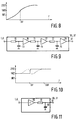
- Fig. 8 shows a non-linear phase shifting characteristic for the phase shifting arrangements 30 and 37 in the embodiment of the present invention having the stopband filters as described.
- the limiters 9 and 13 are replaced by a single limiter for limiting the offset frequency detector output signal ofd2.
- Fig. 9 shows an embodiment of the phase shifting arrangements 30 and 37 of the present invention, implementing the phase shifting characteristic as shown in figure 9.
- the arrangements 30 and 37 comprise a cascade of three RC-shifting sections with respective resistors 70, 71, and 72, respective capacitors 73, 74, and 75, and respective opamps 76, 77, and 78.
- a time constant of the filter sections is ⁇ 3/(2 ⁇ f), for three filter sections.
- the arrangements 30 and 37 may also comprise four RC-shifting sections (not shown).
- Figures 10 and 11 show a third out-of-range extension embodiment of the present invention.
- Fig. 10 shows a phase shifting characteristic in another embodiment of the present invention, a wide stopband filter around the the oscillator frequency f L not being necessary.
- the characteristic exhibits a 180° phase shift for f ⁇ f, and a phase shift of 270° for higher frequencies, but a more gradual phase change will do also, as indicated with a broken line. It holds for ⁇ f ⁇ 0, that either
- > ⁇ f Assuming
- > ⁇ f, during data "0”, the phase shift is 180° with V av 0, and during data "1", the phase shift is 270° with V av having the correct polarity.
- Fig. 11 shows another embodiment of the phase shifting arrangements 30 and 37, implementing the phase shifting characteristic as shown in figure 10.
- the arrangements 30 and 37 comprise an inverting amplifier 80, a resistor 81, and a capacitor 82. It has been shown that for various data duty cycles (the number of data "1"s with respect to the number of data "0"s, on the average) and for various 3 dB frequencies of the phase shifting arrangements 30 and 37, e.g. at 0.5 ⁇ , 0. 67 ⁇ f, ⁇ f, or 2 ⁇ f, that a better performance is achieved for an unequal number of "1"s and "0"s, on the average, for larger 3 dB frequencies, the latter giving rise to a smaller ⁇ f for a.f.c. in-lock.
Landscapes
- Engineering & Computer Science (AREA)
- Computer Networks & Wireless Communication (AREA)
- Signal Processing (AREA)
- Digital Transmission Methods That Use Modulated Carrier Waves (AREA)
Priority Applications (1)
| Application Number | Priority Date | Filing Date | Title |
|---|---|---|---|
| EP19930203239 EP0599414B1 (de) | 1992-11-26 | 1993-11-18 | Direktumsetzempfänger |
Applications Claiming Priority (3)
| Application Number | Priority Date | Filing Date | Title |
|---|---|---|---|
| EP92203653 | 1992-11-26 | ||
| EP92203653 | 1992-11-26 | ||
| EP19930203239 EP0599414B1 (de) | 1992-11-26 | 1993-11-18 | Direktumsetzempfänger |
Publications (3)
| Publication Number | Publication Date |
|---|---|
| EP0599414A2 true EP0599414A2 (de) | 1994-06-01 |
| EP0599414A3 EP0599414A3 (en) | 1995-11-08 |
| EP0599414B1 EP0599414B1 (de) | 2000-08-02 |
Family
ID=26131819
Family Applications (1)
| Application Number | Title | Priority Date | Filing Date |
|---|---|---|---|
| EP19930203239 Expired - Lifetime EP0599414B1 (de) | 1992-11-26 | 1993-11-18 | Direktumsetzempfänger |
Country Status (1)
| Country | Link |
|---|---|
| EP (1) | EP0599414B1 (de) |
Cited By (3)
| Publication number | Priority date | Publication date | Assignee | Title |
|---|---|---|---|---|
| US6148047A (en) * | 1998-05-06 | 2000-11-14 | Philips Electronics North America Corporation | DC offset compensation for zero if quadrature demodulator |
| US6766148B1 (en) * | 2000-03-21 | 2004-07-20 | Koninklijke Phillips Electronics N.V. | Switched sideband frequency low-IF transmitter |
| US8433270B1 (en) | 2011-11-08 | 2013-04-30 | St-Ericsson Sa | Method for tuning an oscillator frequency and device implementing the method |
Families Citing this family (1)
| Publication number | Priority date | Publication date | Assignee | Title |
|---|---|---|---|---|
| RU2754793C1 (ru) * | 2011-11-22 | 2021-09-07 | ООО Научно-производственное предприятие "Новые Технологии Телекоммуникаций" | Устройство для селекции и преобразования частоты модулированных радиосигналов |
Citations (2)
| Publication number | Priority date | Publication date | Assignee | Title |
|---|---|---|---|---|
| GB2180419A (en) * | 1985-09-16 | 1987-03-25 | Philips Electronic Associated | Direct conversion receiver |
| EP0298484A1 (de) * | 1987-07-10 | 1989-01-11 | Siemens Aktiengesellschaft | Optischer FSK-Homodynempfänger |
-
1993
- 1993-11-18 EP EP19930203239 patent/EP0599414B1/de not_active Expired - Lifetime
Patent Citations (2)
| Publication number | Priority date | Publication date | Assignee | Title |
|---|---|---|---|---|
| GB2180419A (en) * | 1985-09-16 | 1987-03-25 | Philips Electronic Associated | Direct conversion receiver |
| EP0298484A1 (de) * | 1987-07-10 | 1989-01-11 | Siemens Aktiengesellschaft | Optischer FSK-Homodynempfänger |
Cited By (3)
| Publication number | Priority date | Publication date | Assignee | Title |
|---|---|---|---|---|
| US6148047A (en) * | 1998-05-06 | 2000-11-14 | Philips Electronics North America Corporation | DC offset compensation for zero if quadrature demodulator |
| US6766148B1 (en) * | 2000-03-21 | 2004-07-20 | Koninklijke Phillips Electronics N.V. | Switched sideband frequency low-IF transmitter |
| US8433270B1 (en) | 2011-11-08 | 2013-04-30 | St-Ericsson Sa | Method for tuning an oscillator frequency and device implementing the method |
Also Published As
| Publication number | Publication date |
|---|---|
| EP0599414A3 (en) | 1995-11-08 |
| EP0599414B1 (de) | 2000-08-02 |
Similar Documents
| Publication | Publication Date | Title |
|---|---|---|
| US5584068A (en) | Direct conversion receiver | |
| CA2014916C (en) | Direct conversion receiver with dithering local carrier frequency for detecting transmitted carrier frequency | |
| US5438692A (en) | Direct conversion receiver | |
| US4523324A (en) | Direct modulation FM data receiver | |
| US4816769A (en) | BPSK demodulator and FM receiver for digital data pagers | |
| US6195400B1 (en) | Two-mode demodulating apparatus | |
| EP0430480A2 (de) | FSK-Verzögerungsdemodulator mit verminderter Offset-Gleichspannung | |
| EP0527469B1 (de) | System zum Empfang von FSK-Daten | |
| US6034990A (en) | Digital radio transmission and reception system applying a direct modulation and demodulation method | |
| US4105975A (en) | Offset correction circuit for phase detectors | |
| EP0161024B1 (de) | FSK-Datenempfänger | |
| KR100427854B1 (ko) | 주파수 안정화된 송/수신 회로 | |
| US4103244A (en) | Fsk demodulator | |
| EP0491421A2 (de) | Kohärenter optischer Vielkanalempfänger | |
| EP0599414B1 (de) | Direktumsetzempfänger | |
| US5612976A (en) | Detectors | |
| EP0599409B1 (de) | Direktumsetzempfänger | |
| EP0259867A2 (de) | Demodulator für PSK-modulierte Signale | |
| US6529565B1 (en) | Circuit for detecting a center error to correct same | |
| US6724247B2 (en) | FM demodulator having DC offset compensation | |
| JPH0638135A (ja) | パルス検出回路 | |
| JP3833259B2 (ja) | Fsk受信器における周波数制御信号の生成 | |
| JP2513329B2 (ja) | 周波数変調波受信装置 | |
| US6621879B1 (en) | Digital radio system, a digital radio device, and a quadrature demodulator | |
| JP2550701B2 (ja) | Fsk受信機 |
Legal Events
| Date | Code | Title | Description |
|---|---|---|---|
| PUAI | Public reference made under article 153(3) epc to a published international application that has entered the european phase |
Free format text: ORIGINAL CODE: 0009012 |
|
| AK | Designated contracting states |
Kind code of ref document: A2 Designated state(s): CH DE FR GB IT LI |
|
| RAP1 | Party data changed (applicant data changed or rights of an application transferred) |
Owner name: N.V. PHILIPS' GLOEILAMPENFABRIEKEN |
|
| PUAL | Search report despatched |
Free format text: ORIGINAL CODE: 0009013 |
|
| AK | Designated contracting states |
Kind code of ref document: A3 Designated state(s): CH DE FR GB IT LI |
|
| 17P | Request for examination filed |
Effective date: 19960508 |
|
| RAP3 | Party data changed (applicant data changed or rights of an application transferred) |
Owner name: KONINKLIJKE PHILIPS ELECTRONICS N.V. |
|
| GRAG | Despatch of communication of intention to grant |
Free format text: ORIGINAL CODE: EPIDOS AGRA |
|
| 17Q | First examination report despatched |
Effective date: 19990920 |
|
| GRAG | Despatch of communication of intention to grant |
Free format text: ORIGINAL CODE: EPIDOS AGRA |
|
| GRAH | Despatch of communication of intention to grant a patent |
Free format text: ORIGINAL CODE: EPIDOS IGRA |
|
| GRAH | Despatch of communication of intention to grant a patent |
Free format text: ORIGINAL CODE: EPIDOS IGRA |
|
| GRAA | (expected) grant |
Free format text: ORIGINAL CODE: 0009210 |
|
| AK | Designated contracting states |
Kind code of ref document: B1 Designated state(s): CH DE FR GB IT LI |
|
| PG25 | Lapsed in a contracting state [announced via postgrant information from national office to epo] |
Ref country code: LI Free format text: LAPSE BECAUSE OF FAILURE TO SUBMIT A TRANSLATION OF THE DESCRIPTION OR TO PAY THE FEE WITHIN THE PRESCRIBED TIME-LIMIT Effective date: 20000802 Ref country code: CH Free format text: LAPSE BECAUSE OF FAILURE TO SUBMIT A TRANSLATION OF THE DESCRIPTION OR TO PAY THE FEE WITHIN THE PRESCRIBED TIME-LIMIT Effective date: 20000802 |
|
| REG | Reference to a national code |
Ref country code: CH Ref legal event code: EP |
|
| REF | Corresponds to: |
Ref document number: 69329140 Country of ref document: DE Date of ref document: 20000907 |
|
| ITF | It: translation for a ep patent filed | ||
| ET | Fr: translation filed | ||
| REG | Reference to a national code |
Ref country code: CH Ref legal event code: PL |
|
| PLBE | No opposition filed within time limit |
Free format text: ORIGINAL CODE: 0009261 |
|
| STAA | Information on the status of an ep patent application or granted ep patent |
Free format text: STATUS: NO OPPOSITION FILED WITHIN TIME LIMIT |
|
| 26N | No opposition filed | ||
| REG | Reference to a national code |
Ref country code: GB Ref legal event code: IF02 |
|
| REG | Reference to a national code |
Ref country code: GB Ref legal event code: 746 Effective date: 20020917 |
|
| REG | Reference to a national code |
Ref country code: FR Ref legal event code: D6 |
|
| PG25 | Lapsed in a contracting state [announced via postgrant information from national office to epo] |
Ref country code: IT Free format text: LAPSE BECAUSE OF NON-PAYMENT OF DUE FEES Effective date: 20051118 |
|
| PGFP | Annual fee paid to national office [announced via postgrant information from national office to epo] |
Ref country code: GB Payment date: 20051129 Year of fee payment: 13 Ref country code: FR Payment date: 20051129 Year of fee payment: 13 |
|
| GBPC | Gb: european patent ceased through non-payment of renewal fee |
Effective date: 20061118 |
|
| REG | Reference to a national code |
Ref country code: FR Ref legal event code: ST Effective date: 20070731 |
|
| PG25 | Lapsed in a contracting state [announced via postgrant information from national office to epo] |
Ref country code: GB Free format text: LAPSE BECAUSE OF NON-PAYMENT OF DUE FEES Effective date: 20061118 |
|
| PG25 | Lapsed in a contracting state [announced via postgrant information from national office to epo] |
Ref country code: FR Free format text: LAPSE BECAUSE OF NON-PAYMENT OF DUE FEES Effective date: 20061130 |
|
| PGFP | Annual fee paid to national office [announced via postgrant information from national office to epo] |
Ref country code: DE Payment date: 20121025 Year of fee payment: 20 |
|
| REG | Reference to a national code |
Ref country code: DE Ref legal event code: R071 Ref document number: 69329140 Country of ref document: DE |
|
| PG25 | Lapsed in a contracting state [announced via postgrant information from national office to epo] |
Ref country code: DE Free format text: LAPSE BECAUSE OF EXPIRATION OF PROTECTION Effective date: 20131119 |