EP0598435A2 - Diskretzeit Signalverarbeitungssystem - Google Patents
Diskretzeit Signalverarbeitungssystem Download PDFInfo
- Publication number
- EP0598435A2 EP0598435A2 EP93203119A EP93203119A EP0598435A2 EP 0598435 A2 EP0598435 A2 EP 0598435A2 EP 93203119 A EP93203119 A EP 93203119A EP 93203119 A EP93203119 A EP 93203119A EP 0598435 A2 EP0598435 A2 EP 0598435A2
- Authority
- EP
- European Patent Office
- Prior art keywords
- frequency
- discrete
- processing system
- signal processing
- signal
- Prior art date
- Legal status (The legal status is an assumption and is not a legal conclusion. Google has not performed a legal analysis and makes no representation as to the accuracy of the status listed.)
- Granted
Links
Images
Classifications
-
- G—PHYSICS
- G11—INFORMATION STORAGE
- G11C—STATIC STORES
- G11C27/00—Electric analogue stores, e.g. for storing instantaneous values
- G11C27/02—Sample-and-hold arrangements
- G11C27/024—Sample-and-hold arrangements using a capacitive memory element
Definitions
- the invention relates to a discrete-time signal processing system comprising a signal sampling circuit and a sampling signal generator whose sampling frequency is adjustable, the sampling signal generator including an oscillator for generating a signal which has a fixed frequency, and a frequency divider.
- the sampling frequency for sampling an analog or digital input signal to be processed is often generated by converting, by means of a frequency divider, a high-frequency output signal of an oscillator into a sampling signal (clock signal) having a lower frequency.
- the oscillation frequency of the oscillator is to be accurate and stable, which is mostly achieved by the use of a crystal oscillator.
- the above means that the sampling frequencies are restricted to f osc /n, where f osc is the oscillation frequency and n the dividend of the frequency divider. If the oscillation frequency f osc is relatively low compared to the clock frequency, this denotes that the clock frequency can be adjusted only in coarse steps.
- the choice of the frequency divider will then determine the oscillation frequency which in many cases does not correspond to the frequencies belonging to the oscillator crystals which are commercially available (and thus cost effective). Furthermore, it may happen that more than one sampling frequency is necessary, such as, for example, in sampling frequency converters. This would require two (precision) oscillators, which is more expensive and more cumbersome compared to a circuit comprising a single oscillator.
- E-A modulator sigma-delta modulator
- the discrete-time signal processing system provides the possibility of selecting with a high degree of freedom a sampling frequency which is derived from a higher clock frequency, whereas the sampling frequency is not restricted to the number of integer dividends.
- n and k are suitably selected, usually n and n + 1, a sampling signal can be generated with a desired frequency, so that its frequency spectrum is such that the frequency spectrum of the sampled signal is not corrupted by the spectrum of the sampling signal.
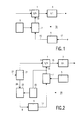
- Fig. 1 shows a discrete-time signal processing system 1 according to the invention, comprising a sample-and-hold circuit 1, a decimation filter 3 connected thereto, an oscillator 5, an adjustable frequency divider 7 and a sigma-delta modulator 9 (to be denoted E-0 modulator hereinafter).
- the sample-and-hold circuit 1 receives on its input 11 a signal to be sampled and receives on a control input 13 a sampling signal i.e. clock signal which is generated by means of the oscillator 5, the frequency divider 7 and the ⁇ - ⁇ modulator 9.
- the signal sampled by the sample-and-hold circuit 1 is further processed by the decimation filter 3.
- the switch-over takes place under the control of the output signal on output 15 of the ⁇ - ⁇ modulator 9 which thereto receives a control signal ⁇ on the input 17.
- This control signal ⁇ may be a DC signal, if the ⁇ - ⁇ modulator 9 is half analog and half digital, or a digital signal which may be one bit or more bits in width.
- Fig. 2 shows a preferred embodiment of a discrete-time signal processing system 20 according to the invention.
- the system 20 comprises an input signal processor 21 and a phase comparator 23 in addition to the components 1, 3, 5, 7 and 9 described with reference to Fig. 1 and having like functions in Fig. 2.
- the input signal processor 21 extracts from a radio stereo signal received on input 27 the audio component, which is applied to the sample-and-hold circuit 1, and the 19 kHz pilot tone, which is applied to the input 29 of the phase comparator 23.
- the phase comparator 23 further receives through a divide-by-two divider 25 the output signal of the frequency divider 7 and forms from these two signals the control signal ⁇ for the ⁇ - ⁇ modulator 9.
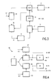
- FIG. 3 A further embodiment of a discrete-time signal processing system 30 according to the invention is shown in Fig. 3, in which all the components corresponding to those of Fig. 2 have like reference numbers and like functions.
- a bandpass filter 31 is inserted, which passes a frequency band around the desired sampling frequency. This achieves an additional reduction of the high-frequency phase-noise in the sampled signal on the control input 13 of the sample-and-hold circuit 1.
- the bandpass filter 31 may be arranged as an analog bandpass filter, for example a ceramic filter, or as an analog phase locked loop, by which loop a large control range can be covered in a relatively simple and cost- effective manner.
- the signal passed by the bandpass filter 31 is applied to a phase comparator 35. Furthermore, an input signal processor 33 is provided which extracts from a received stereo signal the audio component, which is applied to the sample-and-hold circuit 1, and derives from the 19 kHz pilot tone a double frequency signal (38 kHz) which is applied to a phase comparator 35.
- the phase comparator 35 applies a control signal ⁇ to the ⁇ - ⁇ modulator 9.
- Fig. 4 shows a further embodiment of the invention which is preeminently suitable for use in a sampling frequency converter.
- sampling frequency converters the sampling frequency f ; for the incoming signal differs from the sampling frequency f o for the outgoing signal.
- an input clock frequency f i a multiple thereof i.e. clock frequency N.f ; , as well as an output clock frequency f o , is necessary, or an input clock frequency f i , an output clock frequency f o , and a multiple thereof, i.e. clock frequency M.f o .
- the 4 comprises a single (crystal) oscillator 41 whose output signal is applied with the frequency f osc to two frequency dividers 43 and 45.
- the two frequency dividers 43 and 45 are adjustable as regards their dividend i and ii respectively, where n ⁇ i ⁇ n + x and m ⁇ ii ⁇ m + y, where n, m, x and y are positive integers.
- the adjustment in this case the division by either n or n+x and either m or m+y by the frequency dividers 43 and 45 respectively, is determined by the output signal of the ⁇ - ⁇ converters 47 and 51 respectively, which thereto receive an input signal ⁇ 1 and ⁇ 2 respectively.
- the output signals N.f; and M.f o are divided by further frequency dividers 49 and 53 respectively, by a dividend N and M respectively, so that output signals are obtained having the respective desired frequency f i and f o .
- the dividends N and M although being positive integers in this example, need not of necessity be integers considering the above. It should be noted that a sampling frequency converter has been described in a prepublished European Patent Application EP-A-0 512 619.
Landscapes
- Stabilization Of Oscillater, Synchronisation, Frequency Synthesizers (AREA)
- Compression, Expansion, Code Conversion, And Decoders (AREA)
Priority Applications (1)
| Application Number | Priority Date | Filing Date | Title |
|---|---|---|---|
| EP19930203119 EP0598435B1 (de) | 1992-11-13 | 1993-11-08 | Diskretzeit Signalverarbeitungssystem |
Applications Claiming Priority (3)
| Application Number | Priority Date | Filing Date | Title |
|---|---|---|---|
| EP92203487 | 1992-11-13 | ||
| EP92203487 | 1992-11-13 | ||
| EP19930203119 EP0598435B1 (de) | 1992-11-13 | 1993-11-08 | Diskretzeit Signalverarbeitungssystem |
Publications (3)
| Publication Number | Publication Date |
|---|---|
| EP0598435A2 true EP0598435A2 (de) | 1994-05-25 |
| EP0598435A3 EP0598435A3 (en) | 1994-09-28 |
| EP0598435B1 EP0598435B1 (de) | 1998-07-22 |
Family
ID=26131791
Family Applications (1)
| Application Number | Title | Priority Date | Filing Date |
|---|---|---|---|
| EP19930203119 Expired - Lifetime EP0598435B1 (de) | 1992-11-13 | 1993-11-08 | Diskretzeit Signalverarbeitungssystem |
Country Status (1)
| Country | Link |
|---|---|
| EP (1) | EP0598435B1 (de) |
Citations (2)
| Publication number | Priority date | Publication date | Assignee | Title |
|---|---|---|---|---|
| WO1992010033A1 (en) * | 1990-12-03 | 1992-06-11 | Hiro Moriyasu | Signal acquisition system utilizing ultra-wide time range time base |
| EP0512619A1 (de) * | 1991-05-10 | 1992-11-11 | Koninklijke Philips Electronics N.V. | Abtastfrequenzumsetzer |
-
1993
- 1993-11-08 EP EP19930203119 patent/EP0598435B1/de not_active Expired - Lifetime
Patent Citations (2)
| Publication number | Priority date | Publication date | Assignee | Title |
|---|---|---|---|---|
| WO1992010033A1 (en) * | 1990-12-03 | 1992-06-11 | Hiro Moriyasu | Signal acquisition system utilizing ultra-wide time range time base |
| EP0512619A1 (de) * | 1991-05-10 | 1992-11-11 | Koninklijke Philips Electronics N.V. | Abtastfrequenzumsetzer |
Non-Patent Citations (1)
| Title |
|---|
| IBM TECHNICAL DISCLOSURE BULLETIN vol. 21, no. 2 , July 1978 , NEW YORK US pages 452 - 455 'Time of Day Oscillator Circuit' * |
Also Published As
| Publication number | Publication date |
|---|---|
| EP0598435A3 (en) | 1994-09-28 |
| EP0598435B1 (de) | 1998-07-22 |
Similar Documents
| Publication | Publication Date | Title |
|---|---|---|
| US4153876A (en) | Charge transfer device radio system | |
| US4855894A (en) | Frequency converting apparatus | |
| JP2526847B2 (ja) | ディジタル方式無線電話機 | |
| KR100384209B1 (ko) | 단일의국부발진기를가진광주파수스펙트럼텔레비전튜너 | |
| JP2806059B2 (ja) | 位相同期ループシンセサイザ | |
| US6249235B1 (en) | Sampling frequency conversion apparatus and fractional frequency dividing apparatus for sampling frequency | |
| US5019785A (en) | Frequency synthesizing device | |
| JPS60134633A (ja) | 複変換同調器用制御装置 | |
| US6066990A (en) | Frequency divider having a prescaler followed by a programmable counter, and a corresponding prescaler and frequency synthesizer | |
| US5450028A (en) | Discrete-time signal processing system | |
| EP0216803A4 (de) | Digitale zero-mf selektive stufe. | |
| US5857003A (en) | Digital radio having improved modulation and detection processes | |
| JP2002185320A (ja) | 周波数シンセサイザおよび低雑音周波数合成方法 | |
| AU617455B2 (en) | A digital frequency synthesizer | |
| US4878027A (en) | Direct frequency synthesizer using powers of two synthesis techniques | |
| EP0598435B1 (de) | Diskretzeit Signalverarbeitungssystem | |
| EP0454917A1 (de) | Frequenzsynthesizer | |
| US4095190A (en) | Tuning system | |
| JPH1032489A (ja) | ディジタル遅延制御クロック発生器及びこのクロック発生器を使用する遅延ロックループ | |
| GB2317280A (en) | Bandwidth adjustment in phase locked loops | |
| US4547751A (en) | System for frequency modulation | |
| AU674444B2 (en) | Phase detector | |
| KR100277129B1 (ko) | 코드분할다중처리 이동통신단말기의 듀얼모드베이스밴드아날로그 장치 | |
| US5828709A (en) | Apparatus and method for improving stability of transmitting frequency by using costas loop section in communication system of half duplex transmitting method | |
| KR970005394B1 (ko) | 혼합형 주파수 합성기(Hybrid Frequency Synthesizer) |
Legal Events
| Date | Code | Title | Description |
|---|---|---|---|
| PUAI | Public reference made under article 153(3) epc to a published international application that has entered the european phase |
Free format text: ORIGINAL CODE: 0009012 |
|
| AK | Designated contracting states |
Kind code of ref document: A2 Designated state(s): AT DE ES FR GB IT |
|
| PUAL | Search report despatched |
Free format text: ORIGINAL CODE: 0009013 |
|
| RAP1 | Party data changed (applicant data changed or rights of an application transferred) |
Owner name: N.V. PHILIPS' GLOEILAMPENFABRIEKEN |
|
| AK | Designated contracting states |
Kind code of ref document: A3 Designated state(s): AT DE ES FR GB IT |
|
| 17P | Request for examination filed |
Effective date: 19950328 |
|
| 17Q | First examination report despatched |
Effective date: 19970417 |
|
| GRAG | Despatch of communication of intention to grant |
Free format text: ORIGINAL CODE: EPIDOS AGRA |
|
| GRAG | Despatch of communication of intention to grant |
Free format text: ORIGINAL CODE: EPIDOS AGRA |
|
| GRAH | Despatch of communication of intention to grant a patent |
Free format text: ORIGINAL CODE: EPIDOS IGRA |
|
| GRAH | Despatch of communication of intention to grant a patent |
Free format text: ORIGINAL CODE: EPIDOS IGRA |
|
| GRAA | (expected) grant |
Free format text: ORIGINAL CODE: 0009210 |
|
| AK | Designated contracting states |
Kind code of ref document: B1 Designated state(s): AT DE ES FR GB IT |
|
| PG25 | Lapsed in a contracting state [announced via postgrant information from national office to epo] |
Ref country code: IT Free format text: LAPSE BECAUSE OF FAILURE TO SUBMIT A TRANSLATION OF THE DESCRIPTION OR TO PAY THE FEE WITHIN THE PRESCRIBED TIME-LIMIT;WARNING: LAPSES OF ITALIAN PATENTS WITH EFFECTIVE DATE BEFORE 2007 MAY HAVE OCCURRED AT ANY TIME BEFORE 2007. THE CORRECT EFFECTIVE DATE MAY BE DIFFERENT FROM THE ONE RECORDED. Effective date: 19980722 Ref country code: ES Free format text: THE PATENT HAS BEEN ANNULLED BY A DECISION OF A NATIONAL AUTHORITY Effective date: 19980722 Ref country code: AT Free format text: LAPSE BECAUSE OF FAILURE TO SUBMIT A TRANSLATION OF THE DESCRIPTION OR TO PAY THE FEE WITHIN THE PRESCRIBED TIME-LIMIT Effective date: 19980722 |
|
| REF | Corresponds to: |
Ref document number: 168812 Country of ref document: AT Date of ref document: 19980815 Kind code of ref document: T |
|
| RAP4 | Party data changed (patent owner data changed or rights of a patent transferred) |
Owner name: KONINKLIJKE PHILIPS ELECTRONICS N.V. |
|
| REF | Corresponds to: |
Ref document number: 69319851 Country of ref document: DE Date of ref document: 19980827 |
|
| ET | Fr: translation filed | ||
| PLBE | No opposition filed within time limit |
Free format text: ORIGINAL CODE: 0009261 |
|
| STAA | Information on the status of an ep patent application or granted ep patent |
Free format text: STATUS: NO OPPOSITION FILED WITHIN TIME LIMIT |
|
| 26N | No opposition filed | ||
| REG | Reference to a national code |
Ref country code: GB Ref legal event code: IF02 |
|
| REG | Reference to a national code |
Ref country code: GB Ref legal event code: 746 Effective date: 20020917 |
|
| REG | Reference to a national code |
Ref country code: FR Ref legal event code: D6 |
|
| REG | Reference to a national code |
Ref country code: GB Ref legal event code: 732E |
|
| REG | Reference to a national code |
Ref country code: FR Ref legal event code: TP |
|
| PGFP | Annual fee paid to national office [announced via postgrant information from national office to epo] |
Ref country code: FR Payment date: 20101123 Year of fee payment: 18 |
|
| PGFP | Annual fee paid to national office [announced via postgrant information from national office to epo] |
Ref country code: DE Payment date: 20101104 Year of fee payment: 18 |
|
| PGFP | Annual fee paid to national office [announced via postgrant information from national office to epo] |
Ref country code: GB Payment date: 20101103 Year of fee payment: 18 |
|
| GBPC | Gb: european patent ceased through non-payment of renewal fee |
Effective date: 20111108 |
|
| REG | Reference to a national code |
Ref country code: FR Ref legal event code: ST Effective date: 20120731 |
|
| REG | Reference to a national code |
Ref country code: DE Ref legal event code: R119 Ref document number: 69319851 Country of ref document: DE Effective date: 20120601 |
|
| PG25 | Lapsed in a contracting state [announced via postgrant information from national office to epo] |
Ref country code: GB Free format text: LAPSE BECAUSE OF NON-PAYMENT OF DUE FEES Effective date: 20111108 |
|
| PG25 | Lapsed in a contracting state [announced via postgrant information from national office to epo] |
Ref country code: FR Free format text: LAPSE BECAUSE OF NON-PAYMENT OF DUE FEES Effective date: 20111130 |
|
| PG25 | Lapsed in a contracting state [announced via postgrant information from national office to epo] |
Ref country code: DE Free format text: LAPSE BECAUSE OF NON-PAYMENT OF DUE FEES Effective date: 20120601 |