EP0597402B1 - A GaP light emitting element structure - Google Patents
A GaP light emitting element structure Download PDFInfo
- Publication number
- EP0597402B1 EP0597402B1 EP93118011A EP93118011A EP0597402B1 EP 0597402 B1 EP0597402 B1 EP 0597402B1 EP 93118011 A EP93118011 A EP 93118011A EP 93118011 A EP93118011 A EP 93118011A EP 0597402 B1 EP0597402 B1 EP 0597402B1
- Authority
- EP
- European Patent Office
- Prior art keywords
- gap
- light emitting
- layer
- type gap
- type
- Prior art date
- Legal status (The legal status is an assumption and is not a legal conclusion. Google has not performed a legal analysis and makes no representation as to the accuracy of the status listed.)
- Expired - Lifetime
Links
Images



Classifications
-
- H—ELECTRICITY
- H10—SEMICONDUCTOR DEVICES; ELECTRIC SOLID-STATE DEVICES NOT OTHERWISE PROVIDED FOR
- H10H—INORGANIC LIGHT-EMITTING SEMICONDUCTOR DEVICES HAVING POTENTIAL BARRIERS
- H10H20/00—Individual inorganic light-emitting semiconductor devices having potential barriers, e.g. light-emitting diodes [LED]
- H10H20/80—Constructional details
- H10H20/81—Bodies
- H10H20/822—Materials of the light-emitting regions
- H10H20/824—Materials of the light-emitting regions comprising only Group III-V materials, e.g. GaP
- H10H20/8242—Materials of the light-emitting regions comprising only Group III-V materials, e.g. GaP characterised by the dopants
-
- H—ELECTRICITY
- H10—SEMICONDUCTOR DEVICES; ELECTRIC SOLID-STATE DEVICES NOT OTHERWISE PROVIDED FOR
- H10W—GENERIC PACKAGES, INTERCONNECTIONS, CONNECTORS OR OTHER CONSTRUCTIONAL DETAILS OF DEVICES COVERED BY CLASS H10
- H10W72/00—Interconnections or connectors in packages
- H10W72/30—Die-attach connectors
Definitions
- This invention relates to a GaP light emitting element structure, and more specifically to a GaP light emitting element structure comprising a substrate with a plurality of GaP layers on it which is used when manufacturing GaP light emitting diodes which emit green light.
- Light emitting elements such as light emitting diodes are normally obtained by layering a plurality of semiconductor layers on a semiconductor substrate to prepare a multi-layer semiconductor substrate with a pn junction(s), and making this into elements.
- green light emitting diodes can be obtained by using a light emitting element substrate prepared by forming one or more layers of both n-type and p-type GaP layers, one on another, on an n-type GaP single crystal substrate.
- GaP is an indirect transition type semiconductor, and therefore the brightness is very low when a pn junction is simply formed. Therefore nitrogen (N), which would be the luminescence center, is added to the n-type GaP layer in the proximity of the pn junction to increase the light emitting output.
- N nitrogen
- the problem lies in that the brightness of the light emitting diodes varies significantly depending on the manufacturing lot of the buffer layer of the GaP light emitting element which is used in manufacturing the GaP light emitting diodes, and that sufficient brightness may not be achieved depending on the manufacturing lot.
- the buffer layer does not directly contribute to the light emission of a light emitting diode, it seems that the quality of the buffer layer has some kind of influence on the brightness of the light emitting diode. Therefore, the brightness of the light emitting diodes is expected to improve by improving the quality of the buffer layer.
- the object of this invention is to provide a GaP light emitting structure which allows manufacturing of GaP light emitting diodes with less dispersion of the brightness depending on the manufacturing lot of the buffer layer as well as with high brightness.
- the GaP light emitting element structure of this invention comprises an n-type GaP buffer layer, an n-type GaP layer (nitrogen (N), which would be the luminescence center, is added to said layer in the proximity of the pn junction) and a p-type GaP layer layered one on another on an n-type GaP single crystal substrate, characterized by the fact that the oxygen concentration in said n-type GaP buffer layer is made to be 6 x 10 15 atoms/cm 3 or less.
- the inventors earnestly conducted a study to solve the problems described above, and found out that one of the causes of the dispersion of the brightness of the GaP light emitting diodes depending on the manufacturing lot was the dispersion of the transmission characteristics of the n-type GaP buffer for the emitted green light (hereafter referred to as "emitted light").
- emitted light the transmission characteristics of the n-type GaP buffer for the emitted green light
- Figure 1 is a schematic sectional view of an example of a GaP light emitting element structure.
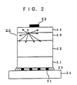
- Figure 2 shows a schematic sectional view of an example of a GaP light emitting diode.
- Figure 3 shows a process diagram which shows an example of a method of manufacturing GaP light emitting element structures.
- Figure 4 shows a graph which shows the relationship between the oxygen concentration in the n-type GaP buffer layer and the transmission ratio of the light with a wavelength of 570 nm.
- Figure 5 is a graph which shows the relationship between the oxygen concentration in the n-type GaP buffer layer and the brightness of the light emitting diodes.
- Figure 1 shows the cross-sectional structure of a GaP light emitting element structure.
- the GaP luminescence element structure 10 comprises an n-type GaP buffer layer 12, an n-type GaP layer 13 (nitrogen (N), which would be the light emitting center, is added to said layer in the proximity of the pn junction) and a p-type GaP layer 14 layered one after another on a GaP single crystal substrate 11.
- N nitrogen
- FIG. 2 shows the cross-sectional structure of a green light emitting GaP light emitting diode 20 manufactured by using said GaP light emitting element structure 10.
- This GaP light emitting diode 20 has the following structure: the light emitting diode chip comprising the GaP light emitting element structure 10 with the n electrode 21 on the side of the n-type GaP single crystal substrate 11 and the p electrode 22 on the side of the p-type GaP layer 14 is adhered to the support member 24 via the conductive paste 23 (Ag paste, for example), and, after wire bonding (not shown in the figure) is carried out, they are sealed with epoxy resin (not shown in the figure).
- the conductive paste 23 Al paste, for example
- green light emission occurs in the proximity of the pn junction and the light is irradiated in all directions as indicated in Figure 2.
- These emitted lights can be divided into the light components X, Y and Z, which are irradiated from the light emitting point toward the surfaces, that is, in the direction of the upper surface (the surface on the side of the p electrode 22), in the direction of the lateral surfaces, and in the direction of the lower surface (the surface of the support member 24), respectively.
- These light components X, Y and Z can be further divided into the light components which are internally absorbed before reaching the surfaces (X 1 , Y 1 and Z 1 ), the light components which reach the surfaces and directly go out (X 2 , Y 2 and Z 2 , except that Z 2 will reflect on the Ag paste surface 23 and go back into the GaP light emitting elements substrate 10), and the light components which reach the surfaces and reflect internally (X 3 , Y 3 and Z 3 ).
- the light components Z 2 , X 3 , Y 3 and Z 3 will either go out after one or multiple reflections, or be absorbed during these reflections.
- the components which would go through said n-type GaP buffer layer 12 once or more times are a part of Y 1 (that is, y 1 ), all of Z 1 , a part of Y 2 (y2), all of Z 2 , a part of X 3 (x 3 ), a part of Y 3 (y 3 ) and all of Z 3 .
- the total of them i.e. y 1 + Z 1 + y 2 + Z 2 + x 3 + y 3 + Z 3 , constitutes a very large portion of the total emitted light.
- the inventors earnestly conducted investigation based on this fact, and found out that the transmission characteristics, for the emitted light, of the n-type GaP buffer layer 12, through which the emitted light has a very high probability of traveling, have a particularly significant influence on the brightness of the light emitting diode.
- the inventor further conducted investigation and found out that the transmission characteristics, for the emitted light, of the n-type GaP buffer layer 12 is influenced by the oxygen concentration in the n-type GaP buffer 12, and that the transmission characteristics for the emitted light improve as the oxygen concentration lowers. That is, a significant correlation between the oxygen concentration in the n-type GaP buffer 12 and the transmission ratio was observed, and the inventors discovered that keeping the oxygen concentration in the n-type GaP buffer low would lead to improved brightness of the light emitting diodes, and thus completed this invention.
- FIG. 3 An example of the GaP light emitting element structure of this invention is described next in detail.
- a Ga solution 16 at 1060°C into which GaP poly-crystals and Te, which is to be an n-type dopant, are dissolved is placed on a GaP single crystal substrate 11.
- This Ga solution 16 is a GaP saturated solution at 1060°C into which Te, which is to be an n-type dopant, is added.
- the temperature of the system which includes said Ga solution 16 is gradually lowered, so that GaP dissolved in the Ga solution 16 precipitates on the n-type GaP single crystal substrate 11.
- the multi-layer GaP substrate 15 comprising the GaP buffer layer 12 doped with Te formed on the n-type GaP single crystal substrate 11 is obtained ( Figure 3 (b)).
- the temperature of the system which contains said fused Ga 17 is raised to 1000°C.
- the upper portion of the n-type GaP buffer layer 12 gradually dissolves into fused Ga 17, and this fused Ga becomes a saturated solution of GaP at 1000°C (Ga solution 17a).
- Te which is contained in the n-type GaP buffer layer 12 also dissolves in said Ga solution 17a ( Figure 3 (d)).
- the temperature is lowered to grow the n-type GaP layer 13 doped with the n-type dopant (Te).
- the flow of NH 3 along with the carrier gas H 2 is introduced for nitrogen (N) doping ( Figure 3 (e)).
- the n-type GaP buffer layer 12, the n-type GaP layer 13, and the p-type GaP layer 14 are formed one after another on the n-type GaP single crystal substrate 11 to prepare the light emitting element structure, and this light emitting element structure is divided into elements to obtain light emitting diodes with green light emission.
- the oxygen concentration in the n-type GaP buffer layer 12 is influenced by, for example, the quality of the Ga solution 16 and the contamination of the growth jigs such as boats which are used to grow each layer. Therefore, in order to keep the oxygen concentration low, it is necessary to use raw materials with low oxygen concentrations for GaP poly-crystals and fused Ga, and to bake the jigs such as boats thoroughly, and it is also necessary to prevent oxidation and adsorption of oxygen and oxides during the process.
- Figure 4 shows the change in the light transmission characteristics depending on the oxygen concentration in the n-type GaP buffer layer. Actual light transmittance measurement was conducted on multi-layer GaP substrates with approximately 150 micrometer thick n-type GaP buffer layers, approximately 50 micrometer thick n-type GaP single crystal substrates, and with a total thickness of approximately 200 micrometers.
- a plurality of multi-layer GaP substrates with various oxygen concentrations in the n-type GaP buffers were prepared, light with a wavelength of 570 nm (equivalent of the emitted light) was applied on the main surfaces of these multi-layer GaP substrates, the quantity of light was measured before and after the transmission for each multi-layer GaP substrate, and the ratio of the quantity of light after the transmission and the quantity of light before the transmission was indicated as a percentage (hereafter, this value is referred to as the "transmission ratio").
- the transmission ratio decreases and it becomes harder for the light with the wavelength of 570 nm (equivalent of the emitted light) to penetrate (the internal absorption increases).
- Figure 5 shows the results of the measurement of the brightness (relative values) of the light emitting diodes which were obtained by, as described above, layering the n-type GaP layer and the p-type GaP layer one on another on each multi-layer GaP substrate which was used for the transmission ratio measurement, and by making it into an element.
- the brightness of the light emitting diode decreases.
- the brightness sharply drops when the oxygen concentration exceeds 6 x 10 15 atoms/cm 3 .
Landscapes
- Led Devices (AREA)
- Led Device Packages (AREA)
Description
- This invention relates to a GaP light emitting element structure, and more specifically to a GaP light emitting element structure comprising a substrate with a plurality of GaP layers on it which is used when manufacturing GaP light emitting diodes which emit green light.
- Light emitting elements such as light emitting diodes are normally obtained by layering a plurality of semiconductor layers on a semiconductor substrate to prepare a multi-layer semiconductor substrate with a pn junction(s), and making this into elements. Of these, green light emitting diodes can be obtained by using a light emitting element substrate prepared by forming one or more layers of both n-type and p-type GaP layers, one on another, on an n-type GaP single crystal substrate.
- GaP is an indirect transition type semiconductor, and therefore the brightness is very low when a pn junction is simply formed. Therefore nitrogen (N), which would be the luminescence center, is added to the n-type GaP layer in the proximity of the pn junction to increase the light emitting output. A light emitting diode prepared from the GaP light emitting element structure which has the nitrogen-doped n-type GaP layer, as described above, will produce a yellow-green light emission with a peak wavelength of about 567 nm.
- Recently, the progress of GaP light emitting diodes which emit green light has been remarkable, and each year diodes with higher light emission outputs are developed. Along with this trend toward higher light emission output, the application range of the GaP light emitting diodes has spread to a very wide range. However, development of light emitting diodes with even higher light emission outputs is desirable in order to further expand the application range.
- However, there is a problem which constitutes an obstacle when designing GaP light emitting diodes with higher brightness. The problem lies in that the brightness of the light emitting diodes varies significantly depending on the manufacturing lot of the buffer layer of the GaP light emitting element which is used in manufacturing the GaP light emitting diodes, and that sufficient brightness may not be achieved depending on the manufacturing lot.
- Although the buffer layer does not directly contribute to the light emission of a light emitting diode, it seems that the quality of the buffer layer has some kind of influence on the brightness of the light emitting diode. Therefore, the brightness of the light emitting diodes is expected to improve by improving the quality of the buffer layer.
- Therefore, the object of this invention is to provide a GaP light emitting structure which allows manufacturing of GaP light emitting diodes with less dispersion of the brightness depending on the manufacturing lot of the buffer layer as well as with high brightness.
- The GaP light emitting element structure of this invention comprises an n-type GaP buffer layer, an n-type GaP layer (nitrogen (N), which would be the luminescence center, is added to said layer in the proximity of the pn junction) and a p-type GaP layer layered one on another on an n-type GaP single crystal substrate, characterized by the fact that the oxygen concentration in said n-type GaP buffer layer is made to be 6 x 10¹⁵ atoms/cm3 or less.
- The inventors earnestly conducted a study to solve the problems described above, and found out that one of the causes of the dispersion of the brightness of the GaP light emitting diodes depending on the manufacturing lot was the dispersion of the transmission characteristics of the n-type GaP buffer for the emitted green light (hereafter referred to as "emitted light"). The relationship between the transmission characteristics of the n-type GaP buffer layer for the emitted light and the brightness of the green light emitting GaP light emitting diodes will be explained below.
- Figure 1 is a schematic sectional view of an example of a GaP light emitting element structure.
- Figure 2 shows a schematic sectional view of an example of a GaP light emitting diode.
- Figure 3 shows a process diagram which shows an example of a method of manufacturing GaP light emitting element structures.
- Figure 4 shows a graph which shows the relationship between the oxygen concentration in the n-type GaP buffer layer and the transmission ratio of the light with a wavelength of 570 nm.
- Figure 5 is a graph which shows the relationship between the oxygen concentration in the n-type GaP buffer layer and the brightness of the light emitting diodes.
- Figure 1 shows the cross-sectional structure of a GaP light emitting element structure. In this figure, the GaP
luminescence element structure 10 comprises an n-typeGaP buffer layer 12, an n-type GaP layer 13 (nitrogen (N), which would be the light emitting center, is added to said layer in the proximity of the pn junction) and a p-type GaP layer 14 layered one after another on a GaPsingle crystal substrate 11. - Figure 2 shows the cross-sectional structure of a green light emitting GaP
light emitting diode 20 manufactured by using said GaP lightemitting element structure 10. This GaPlight emitting diode 20 has the following structure: the light emitting diode chip comprising the GaP lightemitting element structure 10 with then electrode 21 on the side of the n-type GaPsingle crystal substrate 11 and thep electrode 22 on the side of the p-type GaP layer 14 is adhered to thesupport member 24 via the conductive paste 23 (Ag paste, for example), and, after wire bonding (not shown in the figure) is carried out, they are sealed with epoxy resin (not shown in the figure). - When a
forward current 20 is applied to the GaP light emitting diodes as described above, green light emission occurs in the proximity of the pn junction and the light is irradiated in all directions as indicated in Figure 2. These emitted lights can be divided into the light components X, Y and Z, which are irradiated from the light emitting point toward the surfaces, that is, in the direction of the upper surface (the surface on the side of the p electrode 22), in the direction of the lateral surfaces, and in the direction of the lower surface (the surface of the support member 24), respectively. These light components X, Y and Z can be further divided into the light components which are internally absorbed before reaching the surfaces (X1, Y1 and Z1), the light components which reach the surfaces and directly go out (X2, Y2 and Z2, except that Z2 will reflect on theAg paste surface 23 and go back into the GaP light emitting elements substrate 10), and the light components which reach the surfaces and reflect internally (X3, Y3 and Z3). Of these, the light components Z2, X3, Y3 and Z3 will either go out after one or multiple reflections, or be absorbed during these reflections. - Of these emitted light components, the components which would go through said n-type
GaP buffer layer 12 once or more times are a part of Y1 (that is, y1), all of Z1, a part of Y2 (y2), all of Z2, a part of X3 (x3), a part of Y3 (y3) and all of Z3. The total of them, i.e. y1 + Z1 + y2 + Z2 + x3 + y3 + Z3 , constitutes a very large portion of the total emitted light. - The inventors earnestly conducted investigation based on this fact, and found out that the transmission characteristics, for the emitted light, of the n-type
GaP buffer layer 12, through which the emitted light has a very high probability of traveling, have a particularly significant influence on the brightness of the light emitting diode. - The inventor further conducted investigation and found out that the transmission characteristics, for the emitted light, of the n-type
GaP buffer layer 12 is influenced by the oxygen concentration in the n-type GaP buffer 12, and that the transmission characteristics for the emitted light improve as the oxygen concentration lowers. That is, a significant correlation between the oxygen concentration in the n-type GaP buffer 12 and the transmission ratio was observed, and the inventors discovered that keeping the oxygen concentration in the n-type GaP buffer low would lead to improved brightness of the light emitting diodes, and thus completed this invention. - An example of the GaP light emitting element structure of this invention is described next in detail. First, an example of the method of manufacturing the GaP light emitting element structure of this invention is described by referring to Figure 3. As shown in Figure 3 (a), a
Ga solution 16 at 1060°C into which GaP poly-crystals and Te, which is to be an n-type dopant, are dissolved is placed on a GaPsingle crystal substrate 11. ThisGa solution 16 is a GaP saturated solution at 1060°C into which Te, which is to be an n-type dopant, is added. - Then, the temperature of the system which includes said
Ga solution 16 is gradually lowered, so that GaP dissolved in theGa solution 16 precipitates on the n-type GaPsingle crystal substrate 11. Thus, themulti-layer GaP substrate 15 comprising theGaP buffer layer 12 doped with Te formed on the n-type GaPsingle crystal substrate 11 is obtained (Figure 3 (b)). - Next, as shown in Figure 3 (c), fused
Ga 17 without an n-type dopant is placed on saidmulti-layer GaP substrate 15. At this time, the temperature is set at 600°C. - Then, the temperature of the system which contains said fused
Ga 17 is raised to 1000°C. The upper portion of the n-typeGaP buffer layer 12 gradually dissolves into fusedGa 17, and this fused Ga becomes a saturated solution of GaP at 1000°C (Ga solution 17a). Here, Te which is contained in the n-typeGaP buffer layer 12 also dissolves in said Ga solution 17a (Figure 3 (d)). - Next, the temperature is lowered to grow the n-
type GaP layer 13 doped with the n-type dopant (Te). Here, during the second half of the growth process, the flow of NH3 along with the carrier gas H2 is introduced for nitrogen (N) doping (Figure 3 (e)). - Then, the NH3 flow is stopped, the temperature of the system, to which Zn is added here, is raised to about 700°C, and then the temperature is lowered. Thus Zn flows along with the carrier gas H2, and the p-
type GaP layer 14 doped with Zn is formed on the nitrogen-doped n-type GaP layer 13 (Figure 3 (f)). - In the manner described above, the n-type
GaP buffer layer 12, the n-type GaP layer 13, and the p-type GaP layer 14 are formed one after another on the n-type GaPsingle crystal substrate 11 to prepare the light emitting element structure, and this light emitting element structure is divided into elements to obtain light emitting diodes with green light emission. - In the process described above, the oxygen concentration in the n-type
GaP buffer layer 12 is influenced by, for example, the quality of theGa solution 16 and the contamination of the growth jigs such as boats which are used to grow each layer. Therefore, in order to keep the oxygen concentration low, it is necessary to use raw materials with low oxygen concentrations for GaP poly-crystals and fused Ga, and to bake the jigs such as boats thoroughly, and it is also necessary to prevent oxidation and adsorption of oxygen and oxides during the process. - Figure 4 shows the change in the light transmission characteristics depending on the oxygen concentration in the n-type GaP buffer layer. Actual light transmittance measurement was conducted on multi-layer GaP substrates with approximately 150 micrometer thick n-type GaP buffer layers, approximately 50 micrometer thick n-type GaP single crystal substrates, and with a total thickness of approximately 200 micrometers. That is, a plurality of multi-layer GaP substrates with various oxygen concentrations in the n-type GaP buffers were prepared, light with a wavelength of 570 nm (equivalent of the emitted light) was applied on the main surfaces of these multi-layer GaP substrates, the quantity of light was measured before and after the transmission for each multi-layer GaP substrate, and the ratio of the quantity of light after the transmission and the quantity of light before the transmission was indicated as a percentage (hereafter, this value is referred to as the "transmission ratio").
- As shown in the figure, as the oxygen concentration in the n-type GaP buffer layer increases, the transmission ratio decreases and it becomes harder for the light with the wavelength of 570 nm (equivalent of the emitted light) to penetrate (the internal absorption increases).
- Figure 5 shows the results of the measurement of the brightness (relative values) of the light emitting diodes which were obtained by, as described above, layering the n-type GaP layer and the p-type GaP layer one on another on each multi-layer GaP substrate which was used for the transmission ratio measurement, and by making it into an element.
- As shown in the figure, as the oxygen concentration in the n-type GaP buffer layer increases, the brightness of the light emitting diode decreases. In particular, the brightness sharply drops when the oxygen concentration exceeds 6 x 10¹⁵ atoms/cm3.
- This result indicates that, in order to obtain light emitting diodes with high brightness, it is sufficient to keep the oxygen concentration in the n-type GaP buffer layer at 6 x 10¹⁵ atoms/cm3 or less so that the internal absorption is small.
- As described thus far, by using this invention, it is possible to obtain green light emitting GaP light emitting diodes with high brightness by keeping the oxygen concentration in the n-type GaP buffer layer of the GaP light emitting structure at 6 x 10¹⁵ atoms/cm3 or less.
Claims (1)
- A GaP light emitting element structure (10) comprising an n-type GaP buffer layer (12), an n-type GaP layer (13) and a p-type GaP layer (14) layered one on another on an n-type GaP single crystal substrate (11), wherein the oxygen concentration in said n-type GaP buffer layer is 6 x 10¹⁵ atoms/cm3 or less.
Applications Claiming Priority (2)
| Application Number | Priority Date | Filing Date | Title |
|---|---|---|---|
| JP322381/92 | 1992-11-07 | ||
| JP32238192A JP2698891B2 (en) | 1992-11-07 | 1992-11-07 | GaP light emitting device substrate |
Publications (2)
| Publication Number | Publication Date |
|---|---|
| EP0597402A1 EP0597402A1 (en) | 1994-05-18 |
| EP0597402B1 true EP0597402B1 (en) | 1997-03-12 |
Family
ID=18143022
Family Applications (1)
| Application Number | Title | Priority Date | Filing Date |
|---|---|---|---|
| EP93118011A Expired - Lifetime EP0597402B1 (en) | 1992-11-07 | 1993-11-05 | A GaP light emitting element structure |
Country Status (4)
| Country | Link |
|---|---|
| US (1) | US5349208A (en) |
| EP (1) | EP0597402B1 (en) |
| JP (1) | JP2698891B2 (en) |
| DE (1) | DE69308742T2 (en) |
Families Citing this family (5)
| Publication number | Priority date | Publication date | Assignee | Title |
|---|---|---|---|---|
| JP3992117B2 (en) * | 1996-07-18 | 2007-10-17 | 昭和電工株式会社 | GaP light emitting device substrate |
| JP3353703B2 (en) * | 1998-04-30 | 2002-12-03 | 信越半導体株式会社 | Epitaxial wafer and light emitting diode |
| US6664732B2 (en) * | 2000-10-26 | 2003-12-16 | Semiconductor Energy Laboratory Co., Ltd. | Light emitting device and manufacturing method thereof |
| JP2007115874A (en) * | 2005-10-20 | 2007-05-10 | Toyoda Gosei Co Ltd | Structure of bonding pattern, method for forming the same, and light emitting device |
| JP4998396B2 (en) * | 2008-07-22 | 2012-08-15 | 信越半導体株式会社 | Method for manufacturing light emitting device |
Family Cites Families (15)
| Publication number | Priority date | Publication date | Assignee | Title |
|---|---|---|---|---|
| NL6410080A (en) * | 1964-08-29 | 1966-03-01 | ||
| FR1445408A (en) * | 1964-08-29 | 1966-07-08 | Philips Nv | Recombinant injection radiation source |
| US3619304A (en) * | 1968-08-30 | 1971-11-09 | Tokyo Shibaura Electric Co | Method of manufacturing gallium phosphide electro luminescent diodes |
| US3689330A (en) * | 1969-04-18 | 1972-09-05 | Sony Corp | Method of making a luminescent diode |
| BE754437A (en) * | 1969-08-08 | 1971-01-18 | Western Electric Co | IMPROVED ELECTROLUMINESCENT DEVICE |
| US3669767A (en) * | 1969-08-21 | 1972-06-13 | Bell Telephone Labor Inc | Doping profile for gap diodes improved electroluminescent efficiency |
| US3603833A (en) * | 1970-02-16 | 1971-09-07 | Bell Telephone Labor Inc | Electroluminescent junction semiconductor with controllable combination colors |
| US3755006A (en) * | 1971-10-28 | 1973-08-28 | Bell Telephone Labor Inc | Diffused junction gap electroluminescent device |
| US4180423A (en) * | 1974-01-31 | 1979-12-25 | Tokyo Shibaura Electric Co., Ltd. | Method of manufacturing red light-emitting gallium phosphide device |
| JPS5363883A (en) * | 1976-11-18 | 1978-06-07 | Seiko Epson Corp | Monolithic green emission diode display body |
| JPS5382280A (en) * | 1976-12-28 | 1978-07-20 | Toshiba Corp | Gallium phosphide emtting device |
| JPS6028800B2 (en) * | 1977-10-17 | 1985-07-06 | 住友電気工業株式会社 | Low defect density gallium phosphide single crystal |
| JPS55103779A (en) * | 1979-02-02 | 1980-08-08 | Matsushita Electric Ind Co Ltd | Manufacture of light-emitting diode |
| JPH01245569A (en) * | 1988-03-28 | 1989-09-29 | Toshiba Corp | Gap green light-emitting element and manufacture thereof |
| JPH04221862A (en) * | 1990-12-21 | 1992-08-12 | Sharp Corp | Manufacture of gallium phosphide red light emitting diode |
-
1992
- 1992-11-07 JP JP32238192A patent/JP2698891B2/en not_active Expired - Lifetime
-
1993
- 1993-11-05 DE DE69308742T patent/DE69308742T2/en not_active Expired - Fee Related
- 1993-11-05 EP EP93118011A patent/EP0597402B1/en not_active Expired - Lifetime
- 1993-11-05 US US08/147,480 patent/US5349208A/en not_active Expired - Fee Related
Also Published As
| Publication number | Publication date |
|---|---|
| US5349208A (en) | 1994-09-20 |
| EP0597402A1 (en) | 1994-05-18 |
| JP2698891B2 (en) | 1998-01-19 |
| DE69308742T2 (en) | 1997-10-30 |
| JPH06151961A (en) | 1994-05-31 |
| DE69308742D1 (en) | 1997-04-17 |
Similar Documents
| Publication | Publication Date | Title |
|---|---|---|
| US6528823B2 (en) | Semiconductor light-emitting element and method of manufacturing the same | |
| DE4305296C2 (en) | Method of manufacturing a radiation emitting diode | |
| JP3763667B2 (en) | Semiconductor light emitting device | |
| EP1921686A2 (en) | Semiconductor light emitting device and method for manufacturing same | |
| US20020050601A1 (en) | Semiconductor light-emitting device and method of manufacturing the same | |
| US4680602A (en) | Light emitting diode | |
| JPH10107316A (en) | Group III nitride semiconductor light emitting device | |
| EP0616377B1 (en) | Semiconductor light-emitting element and method for its manufacturing | |
| US4212021A (en) | Light emitting devices | |
| US4122486A (en) | Semiconductor light-emitting element | |
| EP0115204B1 (en) | Epitaxial wafer for use in the production of an infrared led | |
| US5349208A (en) | GaP light emitting element substrate with oxygen doped buffer | |
| CA1078949A (en) | Light emitting devices | |
| US6864514B2 (en) | Light emitting diode | |
| CN100426537C (en) | Light emitting diode and method for manufacturing the same | |
| CN1290967A (en) | Luminous diode and its producing method | |
| GB2033155A (en) | Light emissive diode structure | |
| DE112005000675T5 (en) | A compound semiconductor light emitting device and manufacturing method therefor | |
| JP3959434B2 (en) | Light emitting diode element | |
| DE2752107A1 (en) | ELECTROLUMINESC ELEMENT AND METHOD FOR MANUFACTURING IT | |
| RU2154324C1 (en) | Semiconductor infrared radiation source (design versions) | |
| KR100329054B1 (en) | Semiconductor light emitting element and method for fabricating the same | |
| JPH0691280B2 (en) | Semiconductor light emitting diode | |
| US3727115A (en) | Semiconductor electroluminescent diode comprising a ternary compound of gallium, thallium, and phosphorous | |
| JPH1117218A (en) | Semiconductor light emitting device |
Legal Events
| Date | Code | Title | Description |
|---|---|---|---|
| PUAI | Public reference made under article 153(3) epc to a published international application that has entered the european phase |
Free format text: ORIGINAL CODE: 0009012 |
|
| AK | Designated contracting states |
Kind code of ref document: A1 Designated state(s): DE FR GB |
|
| 17P | Request for examination filed |
Effective date: 19940629 |
|
| GRAG | Despatch of communication of intention to grant |
Free format text: ORIGINAL CODE: EPIDOS AGRA |
|
| 17Q | First examination report despatched |
Effective date: 19960306 |
|
| GRAH | Despatch of communication of intention to grant a patent |
Free format text: ORIGINAL CODE: EPIDOS IGRA |
|
| GRAH | Despatch of communication of intention to grant a patent |
Free format text: ORIGINAL CODE: EPIDOS IGRA |
|
| GRAA | (expected) grant |
Free format text: ORIGINAL CODE: 0009210 |
|
| RAP1 | Party data changed (applicant data changed or rights of an application transferred) |
Owner name: SHIN-ETSU HANDOTAI KABUSHIKI KAISHA |
|
| AK | Designated contracting states |
Kind code of ref document: B1 Designated state(s): DE FR GB |
|
| REF | Corresponds to: |
Ref document number: 69308742 Country of ref document: DE Date of ref document: 19970417 |
|
| ET | Fr: translation filed | ||
| PLBE | No opposition filed within time limit |
Free format text: ORIGINAL CODE: 0009261 |
|
| STAA | Information on the status of an ep patent application or granted ep patent |
Free format text: STATUS: NO OPPOSITION FILED WITHIN TIME LIMIT |
|
| 26N | No opposition filed | ||
| PGFP | Annual fee paid to national office [announced via postgrant information from national office to epo] |
Ref country code: GB Payment date: 19981106 Year of fee payment: 6 |
|
| PGFP | Annual fee paid to national office [announced via postgrant information from national office to epo] |
Ref country code: FR Payment date: 19981110 Year of fee payment: 6 |
|
| PGFP | Annual fee paid to national office [announced via postgrant information from national office to epo] |
Ref country code: DE Payment date: 19981116 Year of fee payment: 6 |
|
| PG25 | Lapsed in a contracting state [announced via postgrant information from national office to epo] |
Ref country code: GB Free format text: LAPSE BECAUSE OF NON-PAYMENT OF DUE FEES Effective date: 19991105 |
|
| GBPC | Gb: european patent ceased through non-payment of renewal fee |
Effective date: 19991105 |
|
| PG25 | Lapsed in a contracting state [announced via postgrant information from national office to epo] |
Ref country code: FR Free format text: LAPSE BECAUSE OF NON-PAYMENT OF DUE FEES Effective date: 20000731 |
|
| PG25 | Lapsed in a contracting state [announced via postgrant information from national office to epo] |
Ref country code: DE Free format text: LAPSE BECAUSE OF NON-PAYMENT OF DUE FEES Effective date: 20000901 |
|
| REG | Reference to a national code |
Ref country code: FR Ref legal event code: ST |