EP0595537A1 - Contrôle de l'amplification optique d'un amplificateur optique à semi-conducteur - Google Patents
Contrôle de l'amplification optique d'un amplificateur optique à semi-conducteur Download PDFInfo
- Publication number
- EP0595537A1 EP0595537A1 EP93308336A EP93308336A EP0595537A1 EP 0595537 A1 EP0595537 A1 EP 0595537A1 EP 93308336 A EP93308336 A EP 93308336A EP 93308336 A EP93308336 A EP 93308336A EP 0595537 A1 EP0595537 A1 EP 0595537A1
- Authority
- EP
- European Patent Office
- Prior art keywords
- section
- sections
- input
- output
- semiconductor device
- Prior art date
- Legal status (The legal status is an assumption and is not a legal conclusion. Google has not performed a legal analysis and makes no representation as to the accuracy of the status listed.)
- Granted
Links
Images
Classifications
-
- H—ELECTRICITY
- H01—ELECTRIC ELEMENTS
- H01S—DEVICES USING THE PROCESS OF LIGHT AMPLIFICATION BY STIMULATED EMISSION OF RADIATION [LASER] TO AMPLIFY OR GENERATE LIGHT; DEVICES USING STIMULATED EMISSION OF ELECTROMAGNETIC RADIATION IN WAVE RANGES OTHER THAN OPTICAL
- H01S5/00—Semiconductor lasers
- H01S5/50—Amplifier structures not provided for in groups H01S5/02 - H01S5/30
-
- H—ELECTRICITY
- H01—ELECTRIC ELEMENTS
- H01S—DEVICES USING THE PROCESS OF LIGHT AMPLIFICATION BY STIMULATED EMISSION OF RADIATION [LASER] TO AMPLIFY OR GENERATE LIGHT; DEVICES USING STIMULATED EMISSION OF ELECTROMAGNETIC RADIATION IN WAVE RANGES OTHER THAN OPTICAL
- H01S5/00—Semiconductor lasers
- H01S5/06—Arrangements for controlling the laser output parameters, e.g. by operating on the active medium
- H01S5/062—Arrangements for controlling the laser output parameters, e.g. by operating on the active medium by varying the potential of the electrodes
- H01S5/0625—Arrangements for controlling the laser output parameters, e.g. by operating on the active medium by varying the potential of the electrodes in multi-section lasers
Definitions
- This invention relates generally to semiconductor devices and, more particularly, to a semiconductor device which provides optical gain monitoring when operated as an optical amplifier.
- Semiconductor laser amplifiers are becoming increasingly more important components for optical signal processing applications. In addition to simple loss compensation and switching functions, a semiconductor laser amplifier can provide simultaneous amplification and detection of an optical signal. Recently, amplifiers which exploit this dual capability have demonstrated improved detection capability by employing a split contact and performing the detecting function at the rear contact. See C. Jorgensen et al., "Two-Section Semiconductor Optical Amplifier Used as an Efficient Channel Dropping Node", IEEE Photon. Technol. Letters, Vol. 4, pp. 348-350, 1992.
- This invention is directed toward satisfying this need of monitoring the optical gain of a semiconductor laser amplifier.
- This invention relates to a semiconductor laser amplifier which, in addition to amplifying an optical signal, can also be used for monitoring the amplifier gain. It has been discovered that when a semiconductor laser amplifier is electrically, not optically, split into three separate sections, two end sections and a middle section, and the three sections are forward biased in parallel, the optical gain of the semiconductor amplifier is related to the ratio of the voltages at the two end sections; and this relationship depends only on fixed quantities such as the lengths of the three sections.
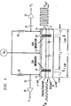
- FIG. 1 schematically illustrates structure according to the invention for monitoring the optical gain of a semiconductor laser amplifier.
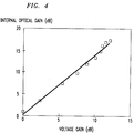
- FIG. 4 is a graphical representation of amplifier internal optical gain vs. voltage gain of the semiconductor laser amplifier.
- the gain of a semiconductor optical amplifier can be monitored by splitting the semiconductor optical amplifier into three electrically isolated sections which extend along a continuous optical waveguide.
- a first section is located at the input end of the amplifier, a second section is located at the output end of the amplifier, and a middle section is located between the first and second sections.
- Each section supports an electrical contact which is used to individually forward bias each section.
- the ratio of the voltages at the contacts coupled to the first or input section and third or output section is related to the gain of the amplifier.
- FIG. 1 there is illustrated a schematic diagram of a semiconductor laser amplifier which provides monitoring of the optical gain.
- the semiconductor amplifier 10 material can be grown using atmospheric pressure metalorganic vapor phase epitaxy.
- the base wafer comprises a strain-compensated 1.55 ⁇ m wavelength multiquantum well gain layer 11 on top of a 280nm (2800 ⁇ ) thick InGaAsP passive waveguide 13 similar to that in B. I. Miller et al., "Strain-Compensated Strained-Layer Superlattices for 1.5 ⁇ m Wavelength Lasers", Appl. Phys. Lett., vol. 58, pp. 1952-1954, 1991.
- the quantum well stack is composed of six 3nm (30 ⁇ ) thick InGaAs wells with 1.3% compressive strain separated by 12.5nm (125 ⁇ ) thick InGaAsP barriers with 0.2% tensile strain having peak photoluminescence wavelength of 1.25 ⁇ m.
- the semiconductor amplifier 10 uses the semi-insulating planar buried-heterostructure as disclosed by U. Koren et al., "Semi-Insulating Blocked Planar Buried Heterostructure GaInAs-InP Laser With High Power and High Modulation Bandwidth", Electron. Lett., vol. 24, pp. 138-139, 1988.
- the semiconductor amplifier 10 is 880 ⁇ m long with the top contact divided into three sections; a 640 ⁇ m middle section 12 and 100 ⁇ m input and output sections 14, 16 at the front and rear facets separated by 20 ⁇ m gaps 18, 20.
- the three sections 12, 14 and 16 are electrically isolated from each other by implanting ions in the gap regions 18, 20. Ions which can be used for this purpose can include, but are not limited to hydrogen, helium and fluorine. With the three sections forward biased, the device was found to have a lasing threshold of 30 mA before the facets are anti-reflection coated.
- n and p are small-signal carrier density and photon density modulation amplitudes
- g n and g are differential gain and unsaturated material gain
- P o is steady-state photon density
- v g is group velocity
- ⁇ sp is carrier spontaneous lifetime.
- n(t) -gv g ⁇ sp p(t).
- Combining relationships (2) and (3) gives v(t) ⁇ p(t).
- the internal Gain G of the amplifier is the ratio of the input and output photon density modulation.
- FIG. 1 there is illustrated a semiconductor amplifier embodying the invention connected to enable its optical gain to be monitored.
- an optical input signal P in from an MQW distributed Bragg reflector laser at 1.561 ⁇ m is directly modulated by a 50 MHz sine wave.
- the light is then attenuated and coupled into the amplifier 10 with an objective lens.
- the input light is TE polarized and, in this instance, the average incident optical power is determined to be -6 dBm.
- the three sections 14, 12, 16 of the semiconductor amplifier 10 are forward biased in parallel; and the ac voltage signals at the contacts of sections 14, 16 are coupled out with a pair of bias tees made up of condensers 22, 24 and inductors 26, 28.
- the ac signal from the contact on top of section 14 is electrically amplified by amplifier 30; and the ac signal from the contact on top of section 16 is electrically amplified by amplifier 32.
- the gain of the semiconductor amplifier is proportional to the ratio of the amplified signals from amplifiers 30, 32.
- the amplified optical signal P out from the semiconductor amplifier 10 is collected with a second objective lens and monitored with an optical power meter, where the detected power from background spontaneous emission is subtracted from the measurement.
- the voltage signals from the contacts on sections 14, 16 are then correlated with the amplifier optical gain.
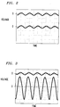
- FIGs. 2 and 3 illustrate typical test results.
- the voltages are measured as a function of amplifier bias current I dc for constant average incident optical power.
- I dc 26mA of bias
- the semiconductor amplifier 10 operated near zero loss where the voltage gain is unity.
- the top plot is the voltage at the input section 14 and the bottom plot in the voltage at the output section 16.
- the voltage gain is 12.1 dB.
- the top plot is the voltage at the input section 14 and the bottom plot is the voltage at the output section 16, shown at half scale.
- FIG. 4 illustrates the internal gain of the semiconductor amplifier 10 vs. voltage gain for the same range of bias currents.
- the optical signal gain at 110 mA of bias is 7.2 dB, and the input coupling loss and ⁇ gap are estimated to be -9 dB and 60cm ⁇ 1 respectively to give 16.2 dB internal gain at the bias current.
- the slope of the line which is independent of estimates for coupling and ⁇ gap , is 1.35, which is slightly higher than the theoretical value of 1.14.
- a more detailed theoretical treatment which includes gain saturation effects could possibly account for the small discrepancy.
Applications Claiming Priority (2)
| Application Number | Priority Date | Filing Date | Title |
|---|---|---|---|
| US967593 | 1992-10-28 | ||
| US07/967,593 US5309469A (en) | 1992-10-28 | 1992-10-28 | Monitoring optical gain of semiconductor optical amplifier |
Publications (2)
| Publication Number | Publication Date |
|---|---|
| EP0595537A1 true EP0595537A1 (fr) | 1994-05-04 |
| EP0595537B1 EP0595537B1 (fr) | 1997-03-19 |
Family
ID=25513020
Family Applications (1)
| Application Number | Title | Priority Date | Filing Date |
|---|---|---|---|
| EP93308336A Expired - Lifetime EP0595537B1 (fr) | 1992-10-28 | 1993-10-20 | ContrÔle de l'amplification optique d'un amplificateur optique à semi-conducteur |
Country Status (4)
| Country | Link |
|---|---|
| US (1) | US5309469A (fr) |
| EP (1) | EP0595537B1 (fr) |
| JP (1) | JP2735474B2 (fr) |
| DE (1) | DE69308984T2 (fr) |
Families Citing this family (6)
| Publication number | Priority date | Publication date | Assignee | Title |
|---|---|---|---|---|
| US5371757A (en) * | 1993-10-22 | 1994-12-06 | The United States Of America As Represented By The Secretary Of The Air Force | Integrated semiconductor laser oscillator and off-axis amplifier |
| EP1130710A3 (fr) * | 2000-01-20 | 2003-09-17 | Cyoptics (Israel) Ltd. | Générateur d'impulsions optiques à taux de répétition élevée |
| US6760350B1 (en) * | 2002-04-12 | 2004-07-06 | The United States Of America As Represented By The National Security Agency | Method for measuring gain of photonic inverters |
| US6771682B2 (en) * | 2002-08-12 | 2004-08-03 | Infinera Corporation | Electrical isolation of optical components in photonic integrated circuits (PICs) |
| KR100617693B1 (ko) * | 2003-08-20 | 2006-08-28 | 삼성전자주식회사 | 광검출기를 구비하는 반도체 광증폭 장치 및 그 제조방법 |
| JP2005135956A (ja) * | 2003-10-28 | 2005-05-26 | Mitsubishi Electric Corp | 半導体光増幅器およびその製造方法ならびに光通信デバイス |
Citations (5)
| Publication number | Priority date | Publication date | Assignee | Title |
|---|---|---|---|---|
| US4523961A (en) * | 1982-11-12 | 1985-06-18 | At&T Bell Laboratories | Method of improving current confinement in semiconductor lasers by inert ion bombardment |
| JPS62291987A (ja) * | 1986-06-12 | 1987-12-18 | Mitsubishi Electric Corp | 光集積化素子 |
| EP0377948A2 (fr) * | 1989-01-12 | 1990-07-18 | Kabushiki Kaisha Toshiba | Dispositif d'amplification optique |
| EP0417989A2 (fr) * | 1989-09-15 | 1991-03-20 | AT&T Corp. | Dispositif à puits quantique et appareil comprenant ce dispositif |
| EP0562518A2 (fr) * | 1992-03-23 | 1993-09-29 | Canon Kabushiki Kaisha | Dispositif optique et méthode d'utilisation, utilisant la variation de tension des bornes d'un région amplificateur |
-
1992
- 1992-10-28 US US07/967,593 patent/US5309469A/en not_active Expired - Lifetime
-
1993
- 1993-10-20 EP EP93308336A patent/EP0595537B1/fr not_active Expired - Lifetime
- 1993-10-20 DE DE69308984T patent/DE69308984T2/de not_active Expired - Lifetime
- 1993-10-26 JP JP5288772A patent/JP2735474B2/ja not_active Expired - Lifetime
Patent Citations (5)
| Publication number | Priority date | Publication date | Assignee | Title |
|---|---|---|---|---|
| US4523961A (en) * | 1982-11-12 | 1985-06-18 | At&T Bell Laboratories | Method of improving current confinement in semiconductor lasers by inert ion bombardment |
| JPS62291987A (ja) * | 1986-06-12 | 1987-12-18 | Mitsubishi Electric Corp | 光集積化素子 |
| EP0377948A2 (fr) * | 1989-01-12 | 1990-07-18 | Kabushiki Kaisha Toshiba | Dispositif d'amplification optique |
| EP0417989A2 (fr) * | 1989-09-15 | 1991-03-20 | AT&T Corp. | Dispositif à puits quantique et appareil comprenant ce dispositif |
| EP0562518A2 (fr) * | 1992-03-23 | 1993-09-29 | Canon Kabushiki Kaisha | Dispositif optique et méthode d'utilisation, utilisant la variation de tension des bornes d'un région amplificateur |
Non-Patent Citations (3)
| Title |
|---|
| C. JORGENSEN ET AL.: "Two-Section Semiconductor Optical Amplifier Used as an Efficient Channel Dropping Node", IEEE PHOTONICS TECHNOLOGY LETTERS, vol. 4, no. 4, April 1992 (1992-04-01), NEW YORK, US, pages 348 - 351, XP000272610 * |
| PATENT ABSTRACTS OF JAPAN vol. 12, no. 189 (E - 616) 2 June 1988 (1988-06-02) * |
| R.M. FORTENBERRY ET AL.: "Up to 16dB Improvement in Detected Voltage Using Two-Section Semiconductor Optical Amplifier Detector", ELECTRONICS LETTERS, vol. 28, no. 5, 27 February 1992 (1992-02-27), STEVENAGE, GB, pages 474 - 476 * |
Also Published As
| Publication number | Publication date |
|---|---|
| DE69308984D1 (de) | 1997-04-24 |
| DE69308984T2 (de) | 1997-07-03 |
| JPH06216434A (ja) | 1994-08-05 |
| US5309469A (en) | 1994-05-03 |
| EP0595537B1 (fr) | 1997-03-19 |
| JP2735474B2 (ja) | 1998-04-02 |
Similar Documents
| Publication | Publication Date | Title |
|---|---|---|
| Park et al. | A hybrid AlGaInAs–silicon evanescent amplifier | |
| Saitoh et al. | 1.5 µm GaInAsP traveling-wave semiconductor laser amplifier | |
| Magari et al. | Polarization-insensitive optical amplifier with tensile-strained-barrier MQW structure | |
| JPH04229684A (ja) | モノリシック集積半導体光前置増幅器 | |
| US8179592B2 (en) | Semiconductor optical amplifier, method for manufacturing the same, and semiconductor optical integrated device | |
| Dutta et al. | Linewidth enhancement factor for InGaAs/InP strained quantum well lasers | |
| Cooper et al. | Broadband operation of InGaAsP-InGaAs GRINSCH MQW amplifiers with 115mW saturated output power | |
| CA2014937C (fr) | Ensemble laser-photodetecteur | |
| Wu et al. | InGaAsP/InP vertical directional coupler filter with optimally designed wavelength tunability | |
| EP0595537B1 (fr) | ContrÔle de l'amplification optique d'un amplificateur optique à semi-conducteur | |
| Loh et al. | Noise figure of Watt-class ultralow-confinement semiconductor optical amplifiers | |
| CA2014938C (fr) | Ensemble amplificateur optique-photodetecteur | |
| Kitamura et al. | Polarization-insensitive semiconductor optical amplifier array grown by selective MOVPE | |
| JPH08250821A (ja) | 半導体光ソース | |
| US4939474A (en) | Semiconductor optical amplifier with shortened gain recovery time | |
| Newkirk et al. | Three-section semiconductor optical amplifier for monitoring of optical gain | |
| Buus et al. | A theoretical and experimental investigation of Fabry-Perot semiconductor laser amplifiers | |
| Sysak et al. | A single regrowth integration platform for photonic circuits incorporating tunable SGDBR lasers and quantum-well EAMs | |
| Rampone et al. | Semiconductor optical amplifier used as an in-line detector with the signal DC-component conservation | |
| US5291328A (en) | Semiconductor laser amplifiers | |
| EP0356189B1 (fr) | Amplificateur optique à semi-conducteur avec durée de rétablissement du gain réduite | |
| Eliseev et al. | Semiconductor optical amplifiers: Multifunctional possibilities, photoresponse and phase shift properties | |
| Dutta et al. | Performance comparison of InGaAsP lasers emitting at 1.3 and 1.55 μm for lightwave system applications | |
| Chawki et al. | Two-electrode DFB laser filter used as a wide tunable narrow-band FM receiver: tuning analysis, characteristics and experimental FSK-WDM system | |
| Doussiere et al. | New laser structure for polarization insensitive semiconductor amplifier with low current consumption |
Legal Events
| Date | Code | Title | Description |
|---|---|---|---|
| PUAI | Public reference made under article 153(3) epc to a published international application that has entered the european phase |
Free format text: ORIGINAL CODE: 0009012 |
|
| AK | Designated contracting states |
Kind code of ref document: A1 Designated state(s): DE FR GB NL |
|
| RAP3 | Party data changed (applicant data changed or rights of an application transferred) |
Owner name: AT&T CORP. |
|
| 17P | Request for examination filed |
Effective date: 19941021 |
|
| GRAG | Despatch of communication of intention to grant |
Free format text: ORIGINAL CODE: EPIDOS AGRA |
|
| GRAH | Despatch of communication of intention to grant a patent |
Free format text: ORIGINAL CODE: EPIDOS IGRA |
|
| 17Q | First examination report despatched |
Effective date: 19960802 |
|
| GRAH | Despatch of communication of intention to grant a patent |
Free format text: ORIGINAL CODE: EPIDOS IGRA |
|
| GRAA | (expected) grant |
Free format text: ORIGINAL CODE: 0009210 |
|
| AK | Designated contracting states |
Kind code of ref document: B1 Designated state(s): DE FR GB NL |
|
| ET | Fr: translation filed | ||
| REF | Corresponds to: |
Ref document number: 69308984 Country of ref document: DE Date of ref document: 19970424 |
|
| PLBE | No opposition filed within time limit |
Free format text: ORIGINAL CODE: 0009261 |
|
| STAA | Information on the status of an ep patent application or granted ep patent |
Free format text: STATUS: NO OPPOSITION FILED WITHIN TIME LIMIT |
|
| 26N | No opposition filed | ||
| PGFP | Annual fee paid to national office [announced via postgrant information from national office to epo] |
Ref country code: NL Payment date: 20000925 Year of fee payment: 8 |
|
| PGFP | Annual fee paid to national office [announced via postgrant information from national office to epo] |
Ref country code: FR Payment date: 20010925 Year of fee payment: 9 |
|
| REG | Reference to a national code |
Ref country code: GB Ref legal event code: IF02 |
|
| PG25 | Lapsed in a contracting state [announced via postgrant information from national office to epo] |
Ref country code: NL Free format text: LAPSE BECAUSE OF NON-PAYMENT OF DUE FEES Effective date: 20020501 |
|
| NLV4 | Nl: lapsed or anulled due to non-payment of the annual fee |
Effective date: 20020501 |
|
| PG25 | Lapsed in a contracting state [announced via postgrant information from national office to epo] |
Ref country code: FR Free format text: LAPSE BECAUSE OF NON-PAYMENT OF DUE FEES Effective date: 20030630 |
|
| REG | Reference to a national code |
Ref country code: FR Ref legal event code: ST |
|
| PGFP | Annual fee paid to national office [announced via postgrant information from national office to epo] |
Ref country code: DE Payment date: 20121017 Year of fee payment: 20 |
|
| PGFP | Annual fee paid to national office [announced via postgrant information from national office to epo] |
Ref country code: GB Payment date: 20121017 Year of fee payment: 20 |
|
| REG | Reference to a national code |
Ref country code: DE Ref legal event code: R071 Ref document number: 69308984 Country of ref document: DE |
|
| REG | Reference to a national code |
Ref country code: GB Ref legal event code: PE20 Expiry date: 20131019 |
|
| PG25 | Lapsed in a contracting state [announced via postgrant information from national office to epo] |
Ref country code: DE Free format text: LAPSE BECAUSE OF EXPIRATION OF PROTECTION Effective date: 20131022 Ref country code: GB Free format text: LAPSE BECAUSE OF EXPIRATION OF PROTECTION Effective date: 20131019 |