EP0594706B1 - Method of producing flat ecr layer in microwave plasma device and apparatus therefor - Google Patents
Method of producing flat ecr layer in microwave plasma device and apparatus therefor Download PDFInfo
- Publication number
- EP0594706B1 EP0594706B1 EP92915157A EP92915157A EP0594706B1 EP 0594706 B1 EP0594706 B1 EP 0594706B1 EP 92915157 A EP92915157 A EP 92915157A EP 92915157 A EP92915157 A EP 92915157A EP 0594706 B1 EP0594706 B1 EP 0594706B1
- Authority
- EP
- European Patent Office
- Prior art keywords
- electromagnet
- electromagnets
- plasma
- chamber
- magnetic field
- Prior art date
- Legal status (The legal status is an assumption and is not a legal conclusion. Google has not performed a legal analysis and makes no representation as to the accuracy of the status listed.)
- Revoked
Links
- 238000000034 method Methods 0.000 title claims abstract description 25
- 238000006243 chemical reaction Methods 0.000 claims abstract description 39
- 230000004907 flux Effects 0.000 claims abstract description 14
- 230000005684 electric field Effects 0.000 claims abstract description 8
- 230000007423 decrease Effects 0.000 claims abstract description 3
- 239000000758 substrate Substances 0.000 claims description 5
- 238000009826 distribution Methods 0.000 description 14
- XEEYBQQBJWHFJM-UHFFFAOYSA-N Iron Chemical compound [Fe] XEEYBQQBJWHFJM-UHFFFAOYSA-N 0.000 description 10
- 239000007789 gas Substances 0.000 description 9
- 238000004364 calculation method Methods 0.000 description 7
- 238000000605 extraction Methods 0.000 description 5
- 229910052742 iron Inorganic materials 0.000 description 5
- 238000010521 absorption reaction Methods 0.000 description 4
- 230000003247 decreasing effect Effects 0.000 description 4
- 230000005284 excitation Effects 0.000 description 4
- 238000004088 simulation Methods 0.000 description 4
- 238000005530 etching Methods 0.000 description 3
- 230000035699 permeability Effects 0.000 description 3
- XKRFYHLGVUSROY-UHFFFAOYSA-N Argon Chemical compound [Ar] XKRFYHLGVUSROY-UHFFFAOYSA-N 0.000 description 2
- 230000015572 biosynthetic process Effects 0.000 description 2
- 230000001419 dependent effect Effects 0.000 description 2
- 239000010408 film Substances 0.000 description 2
- 238000011144 upstream manufacturing Methods 0.000 description 2
- 229910052786 argon Inorganic materials 0.000 description 1
- 239000002826 coolant Substances 0.000 description 1
- 238000001816 cooling Methods 0.000 description 1
- 239000000498 cooling water Substances 0.000 description 1
- 230000007812 deficiency Effects 0.000 description 1
- 238000011065 in-situ storage Methods 0.000 description 1
- 230000005426 magnetic field effect Effects 0.000 description 1
- 238000004519 manufacturing process Methods 0.000 description 1
- 239000000463 material Substances 0.000 description 1
- 238000005457 optimization Methods 0.000 description 1
- 230000002093 peripheral effect Effects 0.000 description 1
- 238000005086 pumping Methods 0.000 description 1
- 239000004065 semiconductor Substances 0.000 description 1
- 238000004544 sputter deposition Methods 0.000 description 1
- 238000005478 sputtering type Methods 0.000 description 1
- 239000010409 thin film Substances 0.000 description 1
Images





Classifications
-
- H—ELECTRICITY
- H01—ELECTRIC ELEMENTS
- H01J—ELECTRIC DISCHARGE TUBES OR DISCHARGE LAMPS
- H01J37/00—Discharge tubes with provision for introducing objects or material to be exposed to the discharge, e.g. for the purpose of examination or processing thereof
- H01J37/32—Gas-filled discharge tubes
- H01J37/32009—Arrangements for generation of plasma specially adapted for examination or treatment of objects, e.g. plasma sources
- H01J37/32192—Microwave generated discharge
-
- H—ELECTRICITY
- H01—ELECTRIC ELEMENTS
- H01J—ELECTRIC DISCHARGE TUBES OR DISCHARGE LAMPS
- H01J37/00—Discharge tubes with provision for introducing objects or material to be exposed to the discharge, e.g. for the purpose of examination or processing thereof
- H01J37/32—Gas-filled discharge tubes
- H01J37/32431—Constructional details of the reactor
- H01J37/3266—Magnetic control means
- H01J37/32678—Electron cyclotron resonance
Definitions
- the present invention relates to a microwave plasma processing device in the etching and film growth processes.
- the invention relates further to a method of forming a flat ECR- layer in such a microwave plasma generating device. More particularly, the invention is used in the process of manufacturing semiconductor devices.
- the plasma is generated by microwaves with electron cyclotron resonance ("ECR") excitation.
- ECR electron cyclotron resonance
- a highly active plasma can be generated at low gas pressures, ion energies can be selected from a wide range of magnitudes, large ionic currents can be realized, and excellent directionality and homogeneity of ionic currents can be achieved.
- FIG. 1 is a cross-section of a conventional microwave plasma apparatus which is used for etching and which operates on the principle of electron cyclotron resonance excitation initiated by microwaves.
- FIG. 2 shows the constant strength flux density lines exemplary of the magnetic field of the conventional apparatus shown in FIG. 1.
- plasma generating chamber 11 is comprised of cylindrical outer wall 11b which has coolant circuit 11a, upper wall 11c and lower wall 11d.
- Microwave feeding hole 12 is located at the center of upper wall 11c.
- Microwave feeding hole 12 is sealed with microwave feeding window 13 and is connected to a lower end of wave guide 14 at feeding window 13.
- the upper part of wave guide 14 is connected with a microwave generator (not shown).
- a generated microwave is introduced through wave guide 14 and feeding window 13 into plasma generating chamber 11.
- Gas feeding pipe 15 is connected with upper wall 11c.
- Electromagnetic exciting coil 18 is coaxially placed around both plasma generating chamber 11 and the lower end of wave guide 14.
- reaction chamber 17 which is connected with plasma generating chamber 11.
- Pumping hole 20 at the lower wall of reaction chamber 17 is connected with an evacuation system (not shown).
- plasma generating chamber 11 and reaction chamber 17 are evacuated. Following evacuation, gas is fed into plasma generating chamber 11 through gas feeding pipe 15. Electromagnetic coil 18 creates a magnetic field within the apparatus. After formation of the magnetic field, a microwave is introduced into plasma generating chamber 11 through wave guide 14 and microwave feeding window 13. Plasma is then formed as a result of the resonance excitation initiated in the gas inside plasma generating chamber 11 which acts as a microwave resonant cavity.
- the plasma generated is transported and brought into contact with sample surface S in reaction chamber 17 by the force of the diverging magnetic field wherein the magnetic flux density of the magnetic field is decreasing in a direction toward reaction chamber 17 thereby ensuring that the surface of the sample S is etched by the plasma.
- Constant strength magnetic flux density lines 21 of the apparatus shown in FIG. 1 are convex, as shown in FIG. 2, with respect to microwave feeding window 13 in plasma generating chamber 11 and concave with respect to sample S in reaction chamber 17. At the midpoint of a line drawn from feeding window 13 to sample S, constant strength magnetic flux density lines 21 approach complete flatness. The region along axis A where constant strength magnetic flux density lines 21 are flat is small, and the gradient of the magnetic field is steep. With the resulting magnetic field configuration, the ratio of the microwave power absorption efficiency to the amount of plasma is low. Absorption is high at the center of the device causing the plasma density distribution and the stability to be poor.
- the conventional apparatus shown in FIGS. 1 and 2 provides an 875 ⁇ 10 ⁇ 4 T (875G) region which is thin in axial direction A since the device generates a non-flat ECR condition.
- Constant strength magnetic flux density line 22 represents the 875 ⁇ 10 ⁇ 4 T (875G) region.
- a very small area of the ECR layer is flat with respect to a plane perpendicular to axial direction A. As mentioned above, this provides high microwave absorption only at the center of plasma generating chamber 11 with the result that plasma density distribution and stability is poor.
- such an arrangement is referred to as the "non-flat ECR condition.”
- U.S. Patent No. 4,911,814 discloses a thin film forming apparatus and ion source utilizing sputtering with microwave plasma.
- the '814 patent discloses a sputtering type ion source utilizing ECR plasma.
- Several embodiments of the apparatus disclosed in the '814 patent include two vertically spaced-apart electromagnets above and below an entry hole in a side of a plasma chamber through which microwave energy is introduced. The electromagnets are arranged such that a magnetic field sufficient to cause ECR is produced and the magnetic flux passes between two targets in the plasma generating chamber.
- the currents passing through the electromagnets can be 20A each, or the current passing through the electromagnet closest to the reaction chamber can be 20A, whereas the current passing through the other electromagnet can be 10A.
- the '814 patent does not disclose the shape of the ECR layer, nor is there any suggestion of supplying a lower amount of current to the electromagnet located closest to the reaction chamber.
- the invention provides a microwave plasma generating device according to claim 1.
- the microwave generating means preferably supplies microwave energy at 2.45 GHz, and the magnetic field has an 875 ⁇ 10 ⁇ 4 T (875G) region which is thick in the axial direction compared to the 875 ⁇ 10 ⁇ 4 T (875G) region generated by a non-flat ECR condition.
- the magnetic field generating means can comprise a plurality of axially spaced-apart electromagnets, each of the electromagnets having a substantially equal number of coil turns, the electromagnets located closer to a center of the device having a larger diameter than the electromagnets located further from the center of the device.
- the magnetic field generating means can include more than three electromagnets, the diameters of the electromagnets becoming progressively smaller towards opposite axial ends of the device.
- the magnetic field generating means can include a first electromagnet around an axial end of the plasma chamber located furthest from the reaction chamber, a second electromagnet around the plasma chamber and located between the first electromagnet and the specimen stage, and a third electromagnet located such that the specimen stage is between the third electromagnet and the plasma chamber.
- All of the electromagnets can be located outside of the plasma chamber and the reaction chamber. However, one or more electromagnets could be provided within the reaction chamber.
- Each of the electromagnets can be supplied with an adjustable amount of current independent of the other electromagnets. However, some or all of the electromagnets can be connected in series to a common direct current source.
- the magnetic field generating means can include first and second electromagnets having the same diameter, the first and second electromagnets having coils of identical gage, the first and second electromagnets being spaced apart along the axial direction, the first electromagnet having a higher number of coil turns than the second electromagnet, and the first electromagnet being further from the specimen stage than the second electromagnet.
- the magnetic field generating means can include first and second electromagnets having the same diameter, the first and second electromagnets having coils of identical gage wire, the first and second electromagnets being spaced apart along the axial direction, the first and second electromagnets having the same number of coil turns, the first electromagnet being further from the specimen stage than the second electromagnet, the magnetic field generating means including a first direct current power supply electrically connected to the first electromagnet and a second direct current power supply electrically connected to the second electromagnet, and the first power supply supplying an amount of electrical current to the first electromagnet which is greater than an amount of electrical current supplied by the second power supply to the second electromagnet.
- the magnetic field generating means can include first and second electromagnets having coils of identical gage wire, the first and second electromagnets being spaced apart in the axial direction with the first electromagnet being further from the specimen stage than the second electromagnet, the first and second electromagnets having the same number of coil turns, the magnetic field generating means including direct current power supply means electrically connected to the first and second electromagnets, the power supply means supplying the first and second electromagnets with the same amount of electrical current, and the second electromagnet having a diameter which is greater than a diameter of the first electromagnet.
- the invention also provides a method of forming a flat ECR layer in a microwave plasma generating device.
- the device includes a plasma generating chamber into which gas is introduced for generating plasma therein, a microwave introducing system for supplying microwave energy into the plasma generating chamber, a specimen chamber communicated with the plasma generating chamber, a substrate holder in the specimen chamber for supporting a specimen to be treated by plasma generated in the plasma generating chamber, and at least first and second electromagnets.
- the first electromagnet is located further from the substrate holder than the second electromagnet, the first and second electromagnets being spaced apart in an axial direction.
- the method includes the steps of introducing gas into the plasma generating chamber, introducing microwave energy into the plasma generating chamber and generating plasma in the plasma generating chamber, and supplying a first amount of direct current to the first electromagnet and supplying a second amount of direct current to the second electromagnet so as to form a flat ECR layer in the plasma.
- the microwave energy can be introduced at 2.45 GHz so as to provide the ECR resonance conditions with the magnetic field which has an 875 ⁇ 10 ⁇ 4 T (875G) region which is thick in the axial direction compared to the 875 ⁇ 10 ⁇ 4 T (875G) region generated by a non-flat ECR condition.
- the first and second electromagnets can be supplied with different amounts of current.
- the first and second electromagnets can be supplied with the same amounts of current.
- the first and second electromagnets can have the same diameter and have coils of identical gage wire, the first electromagnet having a higher number of coil turns than the second electromagnet, in which case the same amount of current is supplied to the first and second electromagnets.
- the amount of current supplied to the first electromagnet can be greater or less than the amount of current supplied to the second electromagnet provided the number of coil turns of the first electromagnet is sufficient to create the flat ECR condition.
- the first and second electromagnets can have the same diameter and have coils of identical gage wire, with the first and second electromagnets having the same number of coil turns, in which case the amount of electrical current supplied to the first electromagnet is greater than the amount of electrical current supplied to the second electromagnet.
- the first and second electromagnets have coils of identical gage wire and have the same number of coil turns with the second electromagnet having a diameter which is greater than a diameter of the first electromagnet, in which case the first and second electromagnets are supplied with the same amount of electrical current.
- the amount of current supplied to the first electromagnet can be greater or less than the amount of current supplied to the second electromagnet provided the diameter of the second electromagnet is selected so as to create the flat ECR condition.
- a flat ECR condition can be produced with the flat ECR layer extending over at least 50%, preferably at least 75% and even over 85% of the width of the plasma chamber.
- the magnetic field distribution can be changed by adjusting the ampere-turn number distribution of the solenoid coils of the electromagnets, employing a number of solenoid coils of different diameters and/or adjusting currents of the electromagnets.
- a magnetic field with a strength distribution generated according to the aforementioned methods has parallel constant strength magnetic flux density lines and small gradients of the magnetic field in an axial direction (the direction in which the plasma moves from the plasma generating chamber to the reaction chamber).
- an electron cyclotron resonance (ECR) plasma generating device in which a microwave of 2.45 GHz and a magnetic field strength of 875 ⁇ 10 ⁇ 4 T (875G) can generate plasma perpendicular to the microwave electric field such that the microwave power is uniformly absorbed and a uniform density plasma can be generated.
- ECR electron cyclotron resonance
- a flat ECR condition is produced wherein the ECR layer extends perpendicular to the axial direction over at least 50%, preferably 75% and more preferably over 85% of the plasma generating chamber.
- the ECR plasma layer (located along the 875 ⁇ 10 ⁇ 4 T (875G) constant strength magnetic flux density line) can be generated at any position between the inside of the plasma chamber and the sample while maintaining the ECR generating condition constant.
- the ion current density and the generated plasma density each of which are dependent on the plasma generating distance, can be optimized around the sample. Optimization results in a uniform and stable plasma generated across the sample surface.
- FIG. 3 shows a cross-section of a microwave plasma processing device according to the present invention.
- the device includes plasma generating chamber 1, wave guide 2, and reaction chamber 3 with sample stage 7 for holding sample S to be etched or provided with a film and three electromagnets C1, C2 and C3.
- C1 is located around the upper part of chamber 1.
- C2 surrounds plasma chamber 1.
- C3 is located below sample stage 7.
- Each coil is covered with iron to create a magnetic energy saving magnetic circuit.
- Plasma generating chamber 1 has double peripheral walls, which form hollow chamber 1a furnished with cooling water and is configured in such a manner that plasma generating chamber 1 can act as a cavity resonator for microwaves.
- Microwave feeding hole 1c is located in the center of the upper wall, and plasma extraction outlet 1d is located at the center of the lower wall opposite microwave feeding hole 1c.
- Microwave window 1b seals the lower end of wave guide 2 to microwave feeding hole lc while sample stage 7 in reaction chamber 3 is axially aligned so as to face plasma extraction outlet 1d.
- the upper end of wave guide 2 is connected to a microwave generator (not shown) which generates microwaves to be introduced into plasma generating chamber 1.
- Electromagnets C1, C2 and C3 are connected to respective direct current sources 8a, 8b and 8c and form a magnetic field when a direct current is passed through the coils of electromagnets C1, C2 and C3.
- Plasma is generated as a result of introducing gas through line 1g and introducing microwaves through window 1b into plasma generating chamber 1 and energizing electromagnets C1, C2 and C3.
- the apparatus is maintained at subatmospheric pressure by evacuation port 3a located beneath sample holder 7 or at another location such as one side of reaction chamber 3.
- FIG. 4 is representative of the magnetic field distribution which can be produced in the apparatus of FIG. 3.
- electromagnet C2' has a greater diameter than electromagnet C2 in FIG. 3, and electromagnet C3' is located inside reaction chamber 3 whereas electromagnet C3 in FIG. 3 is located outside of reaction chamber 3.
- the magnetic field strength distribution within the apparatus can be adjusted by changing the ampere-turn number distribution of the coils of electromagnets C1, C2 and C3.
- the ratio of the ampere-turn number from C1 to C2 to C3 can be 30:35:10.
- Lines 9 shown in FIG. 4 represent the constant strength magnetic flux density lines (
- constant).
- the microwave electric field is assumed to be horizontal.
- the magnetic field component perpendicular to the electric field is B z where B z is in the Z-direction along axis A.
- are substantially equal except in the region far from the central axis.
- the ion current density obtained is 18 mA/cm with a uniformity of ⁇ 3% in a 200 mm diameter area at the specimen position with a microwave power of 1 kW and an argon gas pressure of 133,3 ⁇ 10 ⁇ 3 Pa (1 mTorr).
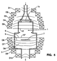
- FIG. 5 shows the magnetic field arrangement with another preferred embodiment of the present invention. Parts having the same function as parts shown in FIG. 3 are identified with the same numerals.
- the coils D1 to D10 of this apparatus are in the form of a cocoon shape. Reaction chamber 3 and the plasma chamber 1 are within the cocoon. Magnetic field strength lines 9 are of equi-magnetic field strength. With this embodiment, a nearly flat magnetic field strength surface can be created with the same currents and numbers of turns for each coil D1 to D10.
- the magnetic field strength distribution can be varied by changing the magnitude of coil current applied to coils D1 to D10 without affecting the shape of the magnetic field distribution. For instance, the coils D1 to D10 can be electrically connected in series, and the ECR layer can be moved from the position represented by line 10' to the line represented by line 10" by increasing the amount of current applied to electromagnets D1 to D10.
- the energizing coils of the plasma generating device are equal in diameter and arranged in a stack of two or more coils.
- the stack could include six coils, as shown in FIG. 6.
- a decreasing current in a direction of movement of plasma generated in the device can be achieved by reducing the number of turns of at least one downstream coil.
- the ratio of turns in an upstream coil to a downstream coil can be any amount such as 6:1, 3:2, 2:1.5, 2:1, etc.
- the ratio of turns of coils E1a:E1b:E1c:E1d:E1e:E1f can be selected such that one of the downstream electromagnets located closer to reaction chamber 3 has a lower number of coils than an upstream electromagnet further from reaction chamber 3.
- Coil E2 can include a stack of sub-coils E2a, E2b and E2c.
- the diameter of coil E2 can exceed the diameter of coils E1a to E1f.
- coil E3 can include a stack of sub-coils E3a, E3b and E3c having diameters intermediate those of coil E1 and coil E2c.
- plasma generating chamber 1 is located below coil E1f.
- rectangular or circular wave guide 2 is connected to larger circular wave guide 2a by tapered adaptor 2b.
- Microwave introducing window 1b seals plasma generating chamber 1 from a lower end of larger wave guide 2a.
- Reaction chamber 3 is not separated from plasma generating chamber by a plasma aperture ring, but, rather, reaction chamber 3 is within the same area the plasma is formed.
- Sample loader 7a is located on one side of plasma generating/reaction chamber 1,3 at a location immediately below coil E2.
- Side evacuation port 3a' is located on another side of plasma generating/reaction chamber 1,3 at a location below coil E2.
- Vertically movable cylinder 7b is used to raise and lower substrate holder 7'.
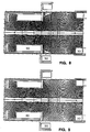
- FIG. 7a shows a conventional main coil arrangement for a plasma generating device wherein the coils are connected in series, each coil has the same number of turns, and the same current, e.g., 20A, is passed therethrough.
- FIG. 7b shows a main coil arrangement in accordance with the invention wherein eight coils having the same number of turns of the same gage wire are connected to separate power supplies such that the coils receive different amounts of current, e.g., 30A, 30A, 20A, 20A, 13A, 13A, 5A, 5A, respectively.
- Line 10 in FIG. 7a represents the non-flat ECR condition of the prior art apparatus whereas line 10 in FIG. 7b shows the flat ECR condition obtainable with the apparatus of the invention.
- main coil F includes sub-coils F1a, F1b, F1c, F1d, F1e, F1f, F1g and F1h surrounding the plasma formation chamber.
- FIGS. 8-14 show simulated magnetic field amplitude lines (
- the simulations apply to the apparatus shown in FIGS. 3, 4, 5, 6 and 7b.
- the coil or coils in main coil E1, the coil or coils in intermediate coil E2, and the coil or coils in lower coil E3 have the same current and ratio of turns in all coils, i.e., 30A in each coil E1, E2 and E3.
- coil E2 has a larger diameter than main coil El, and the magnetic field produced by coil E2 is effective in producing a flat ECR condition, as shown in FIG. 8.
- FIG. 9 shows
- FIGS. 10-13 show
- E1a:E1b:E1c:E2:E3 40:30:10:30:30.
- E1a:E1b:E1c:E2:E3 40:30:10:40:30.
- E1a:E1b:E1c:E2:E3 40:30:10:30:15.
- E1a:E1b:E1c:E2:E3 equals 40:30:10:40:30.
- the arrangement in FIG. 13 differs from that in FIG. 11 with respect to the iron shielding around coil E1.
- FIG. 14 shows a simulation for the cocoon arrangement of coils D1 to D10 shown in FIG. 5.
- the diameters of coils D1 to D5 progressively increase gradually to a maximum diameter towards the center of the device whereas coils D6 to D10 decrease gradually to a minimum diameter.
- the diameters of coils D1 and D10 are the same.
- coils D2 and D9 have the same diameter
- coils D3 and D8 have the same diameter
- coils D4 and D7 have the same diameter
- coils D5 and D6 have the same diameter.
- the ampere-turn ratio in each of coils D1 to D10 is the same.
- the ampere-turn ratio of D1:D2:D3:D4:D5:D6:D7:D8:D9:D10 is 30:30:30:30:30:30:30:30:30:30:30.30.
- B z was 874 ⁇ 10 ⁇ 4, 877 ⁇ 10 ⁇ 4, 877 ⁇ 10 ⁇ 4, 872 ⁇ 10 ⁇ 4 T at radii of 0, 40.2, 75 and 105. Fields were also checked at z values of 247 and 257. These checks indicated ⁇ B z ⁇ z was approximately -4.4 ⁇ 10 ⁇ 4 T/mm (-4.4G/mm) for radii between 0 and 75mm. The linear approximation gives B z strengths of 874 ⁇ 10 ⁇ 4, 870 ⁇ 10 ⁇ 4, and 878 ⁇ 10 ⁇ 4 T (874G, 870G, and 878G) at (0,252), (40.2,252) and (75,252), respectively. Table 1 B fields for coil groups powered at 20A.
Landscapes
- Physics & Mathematics (AREA)
- Engineering & Computer Science (AREA)
- Plasma & Fusion (AREA)
- Chemical & Material Sciences (AREA)
- Analytical Chemistry (AREA)
- Drying Of Semiconductors (AREA)
- Chemical Vapour Deposition (AREA)
- Plasma Technology (AREA)
Abstract
Description
- The present invention relates to a microwave plasma processing device in the etching and film growth processes. The invention relates further to a method of forming a flat ECR- layer in such a microwave plasma generating device. More particularly, the invention is used in the process of manufacturing semiconductor devices. The plasma is generated by microwaves with electron cyclotron resonance ("ECR") excitation.
- Several advantages are realized by devices in which plasma is generated by electron cyclotron resonance excitation. For example, a highly active plasma can be generated at low gas pressures, ion energies can be selected from a wide range of magnitudes, large ionic currents can be realized, and excellent directionality and homogeneity of ionic currents can be achieved.
- FIG. 1 is a cross-section of a conventional microwave plasma apparatus which is used for etching and which operates on the principle of electron cyclotron resonance excitation initiated by microwaves. FIG. 2 shows the constant strength flux density lines exemplary of the magnetic field of the conventional apparatus shown in FIG. 1.
- As shown in FIG. 1,
plasma generating chamber 11 is comprised of cylindricalouter wall 11b which hascoolant circuit 11a,upper wall 11c andlower wall 11d.Microwave feeding hole 12 is located at the center ofupper wall 11c.Microwave feeding hole 12 is sealed withmicrowave feeding window 13 and is connected to a lower end ofwave guide 14 atfeeding window 13. The upper part ofwave guide 14 is connected with a microwave generator (not shown). A generated microwave is introduced throughwave guide 14 andfeeding window 13 intoplasma generating chamber 11.Gas feeding pipe 15 is connected withupper wall 11c. Electromagneticexciting coil 18 is coaxially placed around bothplasma generating chamber 11 and the lower end ofwave guide 14. - At
lower wall 11d ofplasma generating chamber 11, there isplasma extraction window 16. Located belowplasma extraction window 16 isreaction chamber 17 which is connected withplasma generating chamber 11.Sample holder stage 19 for holding wafer S, or some other sample, with an electrostatic chuck, or other conventional means for holding the sample in place, is positioned inreaction chamber 17 facingplasma extraction window 16. Pumpinghole 20 at the lower wall ofreaction chamber 17 is connected with an evacuation system (not shown). - The following describes the operation of an etching process with the above-mentioned conventional microwave plasma apparatus. First,
plasma generating chamber 11 andreaction chamber 17 are evacuated. Following evacuation, gas is fed intoplasma generating chamber 11 throughgas feeding pipe 15.
Electromagnetic coil 18 creates a magnetic field within the apparatus. After formation of the magnetic field, a microwave is introduced intoplasma generating chamber 11 throughwave guide 14 andmicrowave feeding window 13. Plasma is then formed as a result of the resonance excitation initiated in the gas insideplasma generating chamber 11 which acts as a microwave resonant cavity. The plasma generated is transported and brought into contact with sample surface S inreaction chamber 17 by the force of the diverging magnetic field wherein the magnetic flux density of the magnetic field is decreasing in a direction towardreaction chamber 17 thereby ensuring that the surface of the sample S is etched by the plasma. - Constant strength magnetic
flux density lines 21 of the apparatus shown in FIG. 1 are convex, as shown in FIG. 2, with respect tomicrowave feeding window 13 inplasma generating chamber 11 and concave with respect to sample S inreaction chamber 17. At the midpoint of a line drawn fromfeeding window 13 to sample S, constant strength magneticflux density lines 21 approach complete flatness. The region along axis A where constant strength magneticflux density lines 21 are flat is small, and the gradient of the magnetic field is steep. With the resulting magnetic field configuration, the ratio of the microwave power absorption efficiency to the amount of plasma is low. Absorption is high at the center of the device causing the plasma density distribution and the stability to be poor. - The conventional apparatus shown in FIGS. 1 and 2 provides an 875 · 10⁻⁴ T (875G) region which is thin in axial direction A since the device generates a non-flat ECR condition. Constant strength magnetic
flux density line 22 represents the 875 · 10⁻⁴ T (875G) region. In this case, a very small area of the ECR layer is flat with respect to a plane perpendicular to axial direction A. As mentioned above, this provides high microwave absorption only at the center ofplasma generating chamber 11 with the result that plasma density distribution and stability is poor. Hereafter, such an arrangement is referred to as the "non-flat ECR condition." - U.S. Patent No. 4,911,814 ("the '814 patent") discloses a thin film forming apparatus and ion source utilizing sputtering with microwave plasma. In particular, the '814 patent discloses a sputtering type ion source utilizing ECR plasma. Several embodiments of the apparatus disclosed in the '814 patent include two vertically spaced-apart electromagnets above and below an entry hole in a side of a plasma chamber through which microwave energy is introduced. The electromagnets are arranged such that a magnetic field sufficient to cause ECR is produced and the magnetic flux passes between two targets in the plasma generating chamber. The currents passing through the electromagnets can be 20A each, or the current passing through the electromagnet closest to the reaction chamber can be 20A, whereas the current passing through the other electromagnet can be 10A. The '814 patent does not disclose the shape of the ECR layer, nor is there any suggestion of supplying a lower amount of current to the electromagnet located closest to the reaction chamber.
- Other ECR type plasma treating apparatuses are disclosed in U.S. Patent Nos. 4,401,054; 4,438,368; 4,806,829; 4,859,908; 4,947,085; 4,973,883; and 4,990,229.
- There is a need in the art for a microwave plasma generating device which provides a strong, uniform and stable plasma. Applicants have developed an apparatus which produces an improved magnetic field distribution resulting in enhanced microwave power efficiency in the plasma and improved uniformity with respect to plasma density, absorption distribution uniformity.
- The invention provides a microwave plasma generating device according to
claim 1. The microwave generating means preferably supplies microwave energy at 2.45 GHz, and the magnetic field has an 875 · 10⁻⁴ T (875G) region which is thick in the axial direction compared to the 875 · 10⁻⁴ T (875G) region generated by a non-flat ECR condition. - According to one aspect of the invention, the magnetic field generating means can comprise a plurality of axially spaced-apart electromagnets, each of the electromagnets having a substantially equal number of coil turns, the electromagnets located closer to a center of the device having a larger diameter than the electromagnets located further from the center of the device. The magnetic field generating means can include more than three electromagnets, the diameters of the electromagnets becoming progressively smaller towards opposite axial ends of the device.
- According to another aspect of the invention, the magnetic field generating means can include a first electromagnet around an axial end of the plasma chamber located furthest from the reaction chamber, a second electromagnet around the plasma chamber and located between the first electromagnet and the specimen stage, and a third electromagnet located such that the specimen stage is between the third electromagnet and the plasma chamber. All of the electromagnets can be located outside of the plasma chamber and the reaction chamber. However, one or more electromagnets could be provided within the reaction chamber. Each of the electromagnets can be supplied with an adjustable amount of current independent of the other electromagnets. However, some or all of the electromagnets can be connected in series to a common direct current source.
- According to one feature of the invention, the magnetic field generating means can include first and second electromagnets having the same diameter, the first and second electromagnets having coils of identical gage, the first and second electromagnets being spaced apart along the axial direction, the first electromagnet having a higher number of coil turns than the second electromagnet, and the first electromagnet being further from the specimen stage than the second electromagnet.
- According to another feature of the invention, the magnetic field generating means can include first and second electromagnets having the same diameter, the first and second electromagnets having coils of identical gage wire, the first and second electromagnets being spaced apart along the axial direction, the first and second electromagnets having the same number of coil turns, the first electromagnet being further from the specimen stage than the second electromagnet, the magnetic field generating means including a first direct current power supply electrically connected to the first electromagnet and a second direct current power supply electrically connected to the second electromagnet, and the first power supply supplying an amount of electrical current to the first electromagnet which is greater than an amount of electrical current supplied by the second power supply to the second electromagnet.
- According to a still further feature of the invention, the magnetic field generating means can include first and second electromagnets having coils of identical gage wire, the first and second electromagnets being spaced apart in the axial direction with the first electromagnet being further from the specimen stage than the second electromagnet, the first and second electromagnets having the same number of coil turns, the magnetic field generating means including direct current power supply means electrically connected to the first and second electromagnets, the power supply means supplying the first and second electromagnets with the same amount of electrical current, and the second electromagnet having a diameter which is greater than a diameter of the first electromagnet.
- The invention also provides a method of forming a flat ECR layer in a microwave plasma generating device. The device includes a plasma generating chamber into which gas is introduced for generating plasma therein, a microwave introducing system for supplying microwave energy into the plasma generating chamber, a specimen chamber communicated with the plasma generating chamber, a substrate holder in the specimen chamber for supporting a specimen to be treated by plasma generated in the plasma generating chamber, and at least first and second electromagnets. The first electromagnet is located further from the substrate holder than the second electromagnet, the first and second electromagnets being spaced apart in an axial direction. The method includes the steps of introducing gas into the plasma generating chamber, introducing microwave energy into the plasma generating chamber and generating plasma in the plasma generating chamber, and supplying a first amount of direct current to the first electromagnet and supplying a second amount of direct current to the second electromagnet so as to form a flat ECR layer in the plasma. The microwave energy can be introduced at 2.45 GHz so as to provide the ECR resonance conditions with the magnetic field which has an 875 · 10⁻⁴ T (875G) region which is thick in the axial direction compared to the 875 · 10⁻⁴ T (875G) region generated by a non-flat ECR condition.
- According to one aspect of the method, the first and second electromagnets can be supplied with different amounts of current. Alternatively, the first and second electromagnets can be supplied with the same amounts of current. For instance, the first and second electromagnets can have the same diameter and have coils of identical gage wire, the first electromagnet having a higher number of coil turns than the second electromagnet, in which case the same amount of current is supplied to the first and second electromagnets. In this case, however, the amount of current supplied to the first electromagnet can be greater or less than the amount of current supplied to the second electromagnet provided the number of coil turns of the first electromagnet is sufficient to create the flat ECR condition. Alternatively, the first and second electromagnets can have the same diameter and have coils of identical gage wire, with the first and second electromagnets having the same number of coil turns, in which case the amount of electrical current supplied to the first electromagnet is greater than the amount of electrical current supplied to the second electromagnet. Another possibility is where the first and second electromagnets have coils of identical gage wire and have the same number of coil turns with the second electromagnet having a diameter which is greater than a diameter of the first electromagnet, in which case the first and second electromagnets are supplied with the same amount of electrical current. In this case, however, the amount of current supplied to the first electromagnet can be greater or less than the amount of current supplied to the second electromagnet provided the diameter of the second electromagnet is selected so as to create the flat ECR condition. In each case, a flat ECR condition can be produced with the flat ECR layer extending over at least 50%, preferably at least 75% and even over 85% of the width of the plasma chamber.
-
- FIG. 1 shows a cross-section of a conventional plasma generating device;
- FIG. 2 shows the magnetic field strength lines within the FIG. 1 conventional apparatus;
- FIG. 3 shows a cross-section of a plasma generating device according to the present invention;
- FIG. 4 shows magnetic field strength lines within the FIG. 3 apparatus;
- FIG. 5 shows magnetic field strength lines within a modified plasma generating device according to the invention;
- FIG. 6 shows another embodiment of an apparatus in accordance with the invention;
- FIG. 7a shows a conventional main coil electromagnet arrangement which produces a non-flat ECR condition;
- FIG. 7b shows a main coil electromagnet arrangement for producing a flat ECR condition in accordance with the invention; and
- FIGS. 8-14 show simulations of magnetic field amplitude lines in accordance with the invention.
- Applicants have discovered several ways to overcome deficiencies of prior art microwave plasma devices by providing a method and apparatus which produces a flat ECR condition. In particular, the magnetic field distribution can be changed by adjusting the ampere-turn number distribution of the solenoid coils of the electromagnets, employing a number of solenoid coils of different diameters and/or adjusting currents of the electromagnets.
- The above techniques can be used to make an expanded region where the constant strength magnetic flux density lines are flat and parallel to each other. As a result, the field strength of the constructed magnetic field distribution can be changed without altering the distribution pattern by changing the currents of every coil linearly, i.e., in the same proportion. A magnetic field with a strength distribution generated according to the aforementioned methods has parallel constant strength magnetic flux density lines and small gradients of the magnetic field in an axial direction (the direction in which the plasma moves from the plasma generating chamber to the reaction chamber).
- In accordance with the invention, an electron cyclotron resonance (ECR) plasma generating device is provided in which a microwave of 2.45 GHz and a magnetic field strength of 875 · 10⁻⁴ T (875G) can generate plasma perpendicular to the microwave electric field such that the microwave power is uniformly absorbed and a uniform density plasma can be generated. In particular, a flat ECR condition is produced wherein the ECR layer extends perpendicular to the axial direction over at least 50%, preferably 75% and more preferably over 85% of the plasma generating chamber. Also, the ECR plasma layer (located along the 875 · 10⁻⁴ T (875G) constant strength magnetic flux density line) can be generated at any position between the inside of the plasma chamber and the sample while maintaining the ECR generating condition constant. As a result, the ion current density and the generated plasma density, each of which are dependent on the plasma generating distance, can be optimized around the sample. Optimization results in a uniform and stable plasma generated across the sample surface.
- FIG. 3 shows a cross-section of a microwave plasma processing device according to the present invention. The device includes
plasma generating chamber 1,wave guide 2, andreaction chamber 3 withsample stage 7 for holding sample S to be etched or provided with a film and three electromagnets C1, C2 and C3. C1 is located around the upper part ofchamber 1. C2 surroundsplasma chamber 1. C3 is located belowsample stage 7. Each coil is covered with iron to create a magnetic energy saving magnetic circuit. -
Plasma generating chamber 1 has double peripheral walls, which formhollow chamber 1a furnished with cooling water and is configured in such a manner thatplasma generating chamber 1 can act as a cavity resonator for microwaves.Microwave feeding hole 1c is located in the center of the upper wall, andplasma extraction outlet 1d is located at the center of the lower wall oppositemicrowave feeding hole 1c.Microwave window 1b seals the lower end ofwave guide 2 to microwave feeding hole lc whilesample stage 7 inreaction chamber 3 is axially aligned so as to faceplasma extraction outlet 1d. - The upper end of
wave guide 2 is connected to a microwave generator (not shown) which generates microwaves to be introduced intoplasma generating chamber 1. Electromagnets C1, C2 and C3 are connected to respective directcurrent sources window 1b intoplasma generating chamber 1 and energizing electromagnets C1, C2 and C3. The apparatus is maintained at subatmospheric pressure byevacuation port 3a located beneathsample holder 7 or at another location such as one side ofreaction chamber 3. - FIG. 4 is representative of the magnetic field distribution which can be produced in the apparatus of FIG. 3. In FIG. 4, however, electromagnet C2' has a greater diameter than electromagnet C2 in FIG. 3, and electromagnet C3' is located inside
reaction chamber 3 whereas electromagnet C3 in FIG. 3 is located outside ofreaction chamber 3. - The magnetic field strength distribution within the apparatus can be adjusted by changing the ampere-turn number distribution of the coils of electromagnets C1, C2 and C3. For example, the ratio of the ampere-turn number from C1 to C2 to C3 can be 30:35:10.
Lines 9 shown in FIG. 4 represent the constant strength magnetic flux density lines (|B|=constant). The microwave electric field is assumed to be horizontal. The magnetic field component perpendicular to the electric field is Bz where Bz is in the Z-direction along axis A. - The magnetic field strength |B| and |Bz| are substantially equal except in the region far from the central axis. In this embodiment, the ion current density obtained is 18 mA/cm with a uniformity of ± 3% in a 200 mm diameter area at the specimen position with a microwave power of 1 kW and an argon gas pressure of 133,3 · 10⁻³ Pa (1 mTorr).
- FIG. 5 shows the magnetic field arrangement with another preferred embodiment of the present invention. Parts having the same function as parts shown in FIG. 3 are identified with the same numerals. The coils D1 to D10 of this apparatus are in the form of a cocoon shape.
Reaction chamber 3 and theplasma chamber 1 are within the cocoon. Magneticfield strength lines 9 are of equi-magnetic field strength. With this embodiment, a nearly flat magnetic field strength surface can be created with the same currents and numbers of turns for each coil D1 to D10. The magnetic field strength distribution can be varied by changing the magnitude of coil current applied to coils D1 to D10 without affecting the shape of the magnetic field distribution. For instance, the coils D1 to D10 can be electrically connected in series, and the ECR layer can be moved from the position represented by line 10' to the line represented byline 10" by increasing the amount of current applied to electromagnets D1 to D10. - In another embodiment, the energizing coils of the plasma generating device are equal in diameter and arranged in a stack of two or more coils. For instance, the stack could include six coils, as shown in FIG. 6. A decreasing current in a direction of movement of plasma generated in the device can be achieved by reducing the number of turns of at least one downstream coil. For instance, the ratio of turns in an upstream coil to a downstream coil can be any amount such as 6:1, 3:2, 2:1.5, 2:1, etc. With the arrangement shown in FIG. 6, the ratio of turns of coils E1a:E1b:E1c:E1d:E1e:E1f can be selected such that one of the downstream electromagnets located closer to
reaction chamber 3 has a lower number of coils than an upstream electromagnet further fromreaction chamber 3. - Coil E2 can include a stack of sub-coils E2a, E2b and E2c. The diameter of coil E2 can exceed the diameter of coils E1a to E1f. Likewise, coil E3 can include a stack of sub-coils E3a, E3b and E3c having diameters intermediate those of coil E1 and coil E2c.
- As shown in FIG. 6,
plasma generating chamber 1 is located below coil E1f. In particular, rectangular orcircular wave guide 2 is connected to largercircular wave guide 2a by taperedadaptor 2b.Microwave introducing window 1b sealsplasma generating chamber 1 from a lower end oflarger wave guide 2a.Reaction chamber 3 is not separated from plasma generating chamber by a plasma aperture ring, but, rather,reaction chamber 3 is within the same area the plasma is formed.Sample loader 7a is located on one side of plasma generating/reaction chamber Side evacuation port 3a' is located on another side of plasma generating/reaction chamber movable cylinder 7b is used to raise and lower substrate holder 7'. - FIG. 7a shows a conventional main coil arrangement for a plasma generating device wherein the coils are connected in series, each coil has the same number of turns, and the same current, e.g., 20A, is passed therethrough. FIG. 7b shows a main coil arrangement in accordance with the invention wherein eight coils having the same number of turns of the same gage wire are connected to separate power supplies such that the coils receive different amounts of current, e.g., 30A, 30A, 20A, 20A, 13A, 13A, 5A, 5A, respectively.
Line 10 in FIG. 7a represents the non-flat ECR condition of the prior art apparatus whereasline 10 in FIG. 7b shows the flat ECR condition obtainable with the apparatus of the invention. In this case, main coil F includes sub-coils F1a, F1b, F1c, F1d, F1e, F1f, F1g and F1h surrounding the plasma formation chamber. - FIGS. 8-14 show simulated magnetic field amplitude lines (|B| lines) for cases where the magnetic field produced by each of the electromagnets is adjusted in accordance with the invention. The simulations apply to the apparatus shown in FIGS. 3, 4, 5, 6 and 7b. For instance, in FIG. 8, the coil or coils in main coil E1, the coil or coils in intermediate coil E2, and the coil or coils in lower coil E3 have the same current and ratio of turns in all coils, i.e., 30A in each coil E1, E2 and E3. In this case, coil E2 has a larger diameter than main coil El, and the magnetic field produced by coil E2 is effective in producing a flat ECR condition, as shown in FIG. 8. FIG. 9 shows |B| lines for turn ratios or current ratios of E1:E2:E3 of 30:20:30.
- FIGS. 10-13 show |B| lines for the case where the sub-coils in main coil E1 receive decreasing amounts of current or have decreasing ampere-turn ratios. In FIG. 10, E1a:E1b:E1c:E2:E3 equals 40:30:10:30:30. In FIG. 11, E1a:E1b:E1c:E2:E3 equals 40:30:10:40:30. In FIG. 12, E1a:E1b:E1c:E2:E3 equals 40:30:10:30:15. In FIG. 13, E1a:E1b:E1c:E2:E3 equals 40:30:10:40:30. The arrangement in FIG. 13 differs from that in FIG. 11 with respect to the iron shielding around coil E1.
- FIG. 14 shows a simulation for the cocoon arrangement of coils D1 to D10 shown in FIG. 5. The diameters of coils D1 to D5 progressively increase gradually to a maximum diameter towards the center of the device whereas coils D6 to D10 decrease gradually to a minimum diameter. The diameters of coils D1 and D10 are the same. Likewise, coils D2 and D9 have the same diameter, coils D3 and D8 have the same diameter, coils D4 and D7 have the same diameter, and coils D5 and D6 have the same diameter. In this case, the ampere-turn ratio in each of coils D1 to D10 is the same. For instance, the ampere-turn ratio of D1:D2:D3:D4:D5:D6:D7:D8:D9:D10 is 30:30:30:30:30:30:30:30:30:30.
- The following example is for purposes of illustrating various aspects of the invention, it being understood that the same is intended only as illustrative and in no way limitative.
- The following summarizes calculations used to examine the feasibility of running the main coils as a cusp mirror or to obtain a flat ECR layer needed to etch the wafer at the ECR layer.
- For these calculations, the iron around the main coil was taken to have a relative permeability of 500. This is extremely low for iron. Running test calculations with a non-linear B-H relation or with a relative permeability of 1000 changed the calculated magnetic field a few percent. All materials except iron were assigned a relative permeability of 1.0. Coils were treated as an area of uniform current density. The cross-section of this volume was the same as the cross-section of the coil. Total current flow in this area was calculated as the input current multiplied by the number of turns. Coordinates are given as (r,z) pairs. The zero in the coordinate is the end of the coil furthest from the reaction chamber, and z increases towards the reaction chamber. The r coordinate is zero on the chamber centerline. All distances are in millimeters. Br is always zero when r is zero.
- Calculations for the cusp mirror were made by dividing the eight sub-coils of the main coils into two groups. One group consisted of the six coils furthest from the aperture. The other two coils formed the second group. The current in the first group of coils was set at 30A, and the current in the other group was varied. With the bottom coils powered at -40A, the value of Bz went to zero at (0,271) and (100,252). At (50,277) Br is 190 · 10⁻⁴ T (190G), and at (100,277) Br is 500 · 10⁻⁴ T (500G). When the bottom two coils are powered at -25A, the magnetic field in either direction is just a few gauss at any radius and a distance of about 200 mm from the aperture. For both these cases, a continuous Bz= 875 · 10⁻⁴ T (875G) layer forms inside the plasma chamber. This layer is a few cm from the microwave window with the bottom coils powered at -40A and moves forward as this current gets less negative. The results indicate cusp fields can be designed to make magnetic field effects at the wafer insignificant.
- Calculations were made to see what types of coil configurations could yield an ECR layer that occurs at a given z value over a wide radius. The calculations were based on placing an ECR inside the current main coils. In general, Br increases as points get further from the center of the chamber. A flat layer of Bz= 875 · 10⁻⁴ T (875G) will have a greater Br component the further it is from the center of the coil, and Br will increase as radius increases.
- For the flat field problem the main magnet coils were split into three groups, the four coils farthest from the reaction chamber (Group A), the next two coils (Group B), and the two coils closest to the aperture (Group C). Field strengths were estimated by calculating a field solution with 20A in one group of coils and no current in the others. The field at a given z value was recorded at three radii, 0, 40.2 and 75. It was then assumed that the fields for the three groups added linearly. Given this assumption the magnetic field can be estimated and optimized at the points sampled. Table 1 gives the B vector as a function of coil group and location. Currents calculated by solving the approximate equations exactly to give Bz= 875 · 10⁻⁴ T (875G) at the three radii checked at a given z value can be large. The exact solution for z=252 is 43A in Group A, -37.6A in Group B, and 43.4A in Group C. The solution for z=357 is 332A in Group A, -235.4A in Group B, and 72.0A in Group C. There are a large number of current combinations within the current power supply limits that will provide a nearly flat ECR at a given z value. Some of these are shown in Table 2. A complete simulation was done with the current set at 29.3A, 15.1A, 5.3A for Groups A, B and C, respectively. At z=252 Bz was 874 · 10⁻⁴, 877 · 10⁻⁴, 877 · 10⁻⁴, 872 · 10⁻⁴ T at radii of 0, 40.2, 75 and 105. Fields were also checked at z values of 247 and 257. These checks indicated

Table 1 B fields for coil groups powered at 20A. (1G = 10⁻⁴T) Powered Coils Group A Group B Group C At z=252 Br(G) Bz(G) Br(G) Bz(G) Br(G) Bz(G) r=0 0 303 0 409 0 457 r=40.2 55 294 39.6 416 -44.5 472 4=75 103 277 77.2 445 -88.6 514 At z=357 Br(G) Bz(G) Br(G) Bz(G) Br(G) Bz(G) r=0 0 101 0 168 0 326 r=40.2 26.7 94.2 45.4 163 73.6 341 r=75 49.6 81.5 89 146 167 344 
- The calculations indicate that there are a wide range of current configurations that will yield a near flat ECR layer. The optimum configuration will probably be dependent on reducing Br while minimizing the currents and cooling capacity needed for the coils.
- The possibility of making the coils more compact was examined as well. It was found that powering only the three coils closest to the reaction chamber at 30A will provide a continuous ECR layer and a peak field strength of 1030 · 10⁻⁴ T (1030G). This indicates that a magnet of approximately half the size of the current coils should provide enough field strength for in situ ECR etch. If the magnet contains several coils (5 to 10) currents could probably be adjusted to provide a flat ECR layer. If the magnet has an axis of symmetry perpendicular to the z axis and the wafer is centered in the coil, there will be no Br field on the wafer.
- While the invention has been described with reference to the foregoing embodiments, changes and variations may be made thereto which fall within the scope of the appended claims.
Claims (21)
- A microwave plasma generating device, comprising:a plasma chamber for generating plasma;a reaction chamber having a specimen stage on which a specimen is treated with the plasma;gas supply means for supplying gas to the plasma generating chamber;means for generating a microwave electric field in the plasma and reaction chambers;means comprising axially spaced apart and concentric electromagnet coils for generating a magnetic field in the plasma and reaction chambers, the microwave electric field and magnetic field having perpendicularly crossing components of the magnetic field and electric field, respectively, the magnetic field having a strength which decreases in an axial direction from the plasma chamber towards the reaction chamber and having constant strength magnetic flux density lines lying in planes which are substantially parallel to each other and perpendicular to the axial direction, the magnetic field producing a flat ECR condition wherein an ECR layer extends perpendicular to the axial direction over at least 50% of the width of the plasma chamber.
- The microwave plasma generating device of claim 1, wherein the magnetic field generating means comprises a plurality of axially spaced-apart electromagnets having coils concentric with each other, each of the electromagnets having a substantially equal number of coil turns, the electromagnets located closer to a center of the device having a larger diameter than the electromagnets located further from the center of the device.
- The microwave plasma generating device of claim 1, wherein the magnetic field generating means includes a first electromagnet extending completely around an end of the plasma chamber located furthest from the reaction chamber, a second electromagnet extending completely around the plasma chamber and located between the first electromagnet and the specimen stage, and a third electromagnet located such that the specimen stage is between the third electromagnet and the plasma chamber.
- The microwave plasma generating device of claim 2, wherein the magnetic field generating means includes more than three electromagnets, the diameters of the electromagnets becoming progressively smaller towards opposite axial ends of the device.
- The microwave plasma generating device of claim 3, wherein all of the electromagnets are located outside of the plasma chamber and the reaction chamber.
- The microwave plasma generating device of claim 1, wherein the magnetic field generating means includes a plurality of electromagnets having coils concentric with each other and means for supplying each of the electromagnets with an adjustable amount of current independent of the other electromagnets.
- The microwave plasma generating device of claim 1, wherein the magnetic field generating means includes first and second electromagnets having the same diameter, the first and second electromagnets having coils concentric with each other and of identical gage wire, the first and second electromagnets being spaced apart along the axial direction, the first electromagnet having a higher number of coil turns than the second electromagnet and the first electromagnet being further from the specimen stage than the second electromagnet.
- The microwave plasma generating device of claim 1, wherein the magnetic field generating means includes first and second electromagnets having coils concentric with each other having the same diameter, the first and second electromagnets having coils of identical gage wire, the first and second electromagnets being spaced apart along the axial direction, the first and second electromagnets having the same number of coil turns, the first electromagnet being further from the specimen stage than the second electromagnet, the magnetic field generating means including a first direct current power supply electrically connected to the first electromagnet and a second direct current power supply electrically connected to the second electromagnet, and the first power supply supplying an amount of electrical current to the first electromagnet which is greater than an amount of electrical current supplied by the second power supply to the second electromagnet.
- The microwave plasma generating device of claim 1, wherein the magnetic field generating means includes first and second electromagnets having coils concentric with each other and of identical gage wire, the first and second electromagnets being spaced apart in the axial direction with the first electromagnet being further from the specimen stage than the second electromagnet, the first and second electromagnets having the same number of coil turns, the magnetic field generating means including direct current power supply means electrically connected to the first and second electromagnets, the power supply means supplying the first and second electromagnets with the same amount of electrical current, and the second electromagnet having a diameter which is greater than a diameter of the first electromagnet.
- A method of forming a flat ECR layer in a microwave plasma generating device, the device including a plasma generating chamber into which gas is introduced for generating plasma therein, a microwave introducing system for supplying microwave energy into the plasma generating chamber, a specimen chamber communicated with the plasma generating chamber, a substrate holder in the specimen chamber for supporting a specimen to be treated by plasma generated in the plasma generating chamber, and at least first and second electromagnets, the first electromagnet being located further from the substrate holder than the second electromagnet, the first and second electromagnets being spaced apart in an axial direction, the first electromagnet having coils which are concentric with coils of the second electromagnet for generating a magnetic field in the plasma and specimen chambers, the method comprising steps of:introducing gas into the plasma generating chamber;introducing microwave energy into the plasma generating chamber and generating plasma in the plasma generating chamber; andsupplying a first amount of direct current to the first electromagnet and supplying a second amount of direct current to the second electromagnet so as to form constant strength magnetic field flux density lines lying in planes which are substantially parallel to each other and perpendicular to the axial direction and a flat ECR layer in the plasma wherein an ECR layer extends perpendicular to the axial direction over at least 50% of the width of the plasma chamber.
- The method of claim 10, wherein the first and second electromagnets are supplied with different amounts of current.
- The method of claim 10, wherein the first and second electromagnets are supplied with the same amounts of current.
- The method of claim 10, wherein the first and second electromagnets have the same diameter, the first and second electromagnets have coils concentric with each other and of identical gage wire, the first electromagnet has a higher number of coil turns than the second electromagnet and the same amount of current is supplied to the first and second electromagnets.
- The method of claim 10, wherein the first and second electromagnets have the same diameter, the first and second electromagnets have coils concentric with each other and of identical gage wire, the first and second electromagnets have the same number of coil turns, and the amount of electrical current supplied to the first electromagnet is greater than the amount of electrical current supplied to the second electromagnet.
- The method of claim 10, wherein the first and second electromagnets have coils concentric with each other and of identical gage wire, the first and second electromagnets have the same number of coil turns, the second electromagnet has a diameter which is greater than a diameter of the first electromagnet, and the first and second electromagnets are supplied with the same amount of electrical current.
- The method of claim 10, wherein the first and second electromagnets have the same diameter, the first and second electromagnets have coils concentric with each other and of identical gage wire, the first electromagnet has a higher number of coil turns than the second electromagnet and the amount of current supplied to the first electromagnet is less than the amount of current supplied to the second electromagnet.
- The method of claim 10, wherein the first and second electromagnets have the same diameter, the first and second electromagnets have coils concentric with each other and of identical gage wire, the first electromagnet has a higher number of coil turns than the second electromagnet and the amount of current supplied to the first electromagnet is greater than the amount of current supplied to the second electromagnet.
- The method of claim 10, wherein the first and second electromagnets have coils concentric with each other and of identical gage wire, the first and second electromagnets have the same number of coil turns, the second electromagnet has a diameter which is greater than a diameter of the first electromagnet, and the amount of current supplied to the first electromagnet is less than the amount of current supplied to the second electromagnet.
- The method of claim 10, wherein the first and second electromagnets have coils concentric with each other and of identical gage wire, the first and second electromagnets have the same number of coil turns, and the second electromagnet has a diameter which is greater than a diameter of the first electromagnet, and the amount of current supplied to the first electromagnet is greater than the amount of current supplied to the second electromagnet.
- The method of claim 10, wherein the flat ECR layer extends perpendicularly with respect to the axial direction and covers at least 75% of the width of the plasma generating chamber.
- The method of claim 10, wherein the flat ECR layer extends perpendicularly with respect to the axial direction and covers at least 85% of the width of the plasma generating chamber.
Applications Claiming Priority (3)
| Application Number | Priority Date | Filing Date | Title |
|---|---|---|---|
| US07/729,211 US5198725A (en) | 1991-07-12 | 1991-07-12 | Method of producing flat ecr layer in microwave plasma device and apparatus therefor |
| US729211 | 1991-07-12 | ||
| PCT/US1992/005674 WO1993001698A1 (en) | 1991-07-12 | 1992-07-10 | Method of producing flat ecr layer in microwave plasma device and apparatus therefor |
Publications (3)
| Publication Number | Publication Date |
|---|---|
| EP0594706A1 EP0594706A1 (en) | 1994-05-04 |
| EP0594706A4 EP0594706A4 (en) | 1994-08-17 |
| EP0594706B1 true EP0594706B1 (en) | 1996-04-03 |
Family
ID=24930045
Family Applications (1)
| Application Number | Title | Priority Date | Filing Date |
|---|---|---|---|
| EP92915157A Revoked EP0594706B1 (en) | 1991-07-12 | 1992-07-10 | Method of producing flat ecr layer in microwave plasma device and apparatus therefor |
Country Status (4)
| Country | Link |
|---|---|
| US (1) | US5198725A (en) |
| EP (1) | EP0594706B1 (en) |
| DE (1) | DE69209647T2 (en) |
| WO (1) | WO1993001698A1 (en) |
Families Citing this family (72)
| Publication number | Priority date | Publication date | Assignee | Title |
|---|---|---|---|---|
| FR2701797B1 (en) * | 1993-02-18 | 1995-03-31 | Commissariat Energie Atomique | Microwave power transfer coupler to a plasma table and linear microwave source for plasma surface treatment. |
| US6475333B1 (en) * | 1993-07-26 | 2002-11-05 | Nihon Shinku Gijutsu Kabushiki Kaisha | Discharge plasma processing device |
| US5759922A (en) * | 1993-08-25 | 1998-06-02 | Micron Technology, Inc. | Control of etch profiles during extended overetch |
| JPH07142444A (en) * | 1993-11-12 | 1995-06-02 | Hitachi Ltd | Microwave plasma processing apparatus and processing method |
| US5435881A (en) * | 1994-03-17 | 1995-07-25 | Ogle; John S. | Apparatus for producing planar plasma using varying magnetic poles |
| US5503676A (en) * | 1994-09-19 | 1996-04-02 | Lam Research Corporation | Apparatus and method for magnetron in-situ cleaning of plasma reaction chamber |
| US5556521A (en) * | 1995-03-24 | 1996-09-17 | Sony Corporation | Sputter etching apparatus with plasma source having a dielectric pocket and contoured plasma source |
| US5653811A (en) | 1995-07-19 | 1997-08-05 | Chan; Chung | System for the plasma treatment of large area substrates |
| TW303480B (en) * | 1996-01-24 | 1997-04-21 | Applied Materials Inc | Magnetically confined plasma reactor for processing a semiconductor wafer |
| US5824607A (en) * | 1997-02-06 | 1998-10-20 | Applied Materials, Inc. | Plasma confinement for an inductively coupled plasma reactor |
| US6210539B1 (en) * | 1997-05-14 | 2001-04-03 | Applied Materials, Inc. | Method and apparatus for producing a uniform density plasma above a substrate |
| US6077402A (en) * | 1997-05-16 | 2000-06-20 | Applied Materials, Inc. | Central coil design for ionized metal plasma deposition |
| US6361661B2 (en) | 1997-05-16 | 2002-03-26 | Applies Materials, Inc. | Hybrid coil design for ionized deposition |
| US6274459B1 (en) | 1998-02-17 | 2001-08-14 | Silicon Genesis Corporation | Method for non mass selected ion implant profile control |
| US6506287B1 (en) | 1998-03-16 | 2003-01-14 | Applied Materials, Inc. | Overlap design of one-turn coil |
| US6146508A (en) * | 1998-04-22 | 2000-11-14 | Applied Materials, Inc. | Sputtering method and apparatus with small diameter RF coil |
| US6123862A (en) * | 1998-04-24 | 2000-09-26 | Micron Technology, Inc. | Method of forming high aspect ratio apertures |
| US6204607B1 (en) | 1998-05-28 | 2001-03-20 | Applied Komatsu Technology, Inc. | Plasma source with multiple magnetic flux sources each having a ferromagnetic core |
| JP2000021871A (en) * | 1998-06-30 | 2000-01-21 | Tokyo Electron Ltd | Plasma processing method |
| US6660134B1 (en) | 1998-07-10 | 2003-12-09 | Applied Materials, Inc. | Feedthrough overlap coil |
| US6217718B1 (en) | 1999-02-17 | 2001-04-17 | Applied Materials, Inc. | Method and apparatus for reducing plasma nonuniformity across the surface of a substrate in apparatus for producing an ionized metal plasma |
| US6458723B1 (en) | 1999-06-24 | 2002-10-01 | Silicon Genesis Corporation | High temperature implant apparatus |
| US6528751B1 (en) | 2000-03-17 | 2003-03-04 | Applied Materials, Inc. | Plasma reactor with overhead RF electrode tuned to the plasma |
| US20070048882A1 (en) * | 2000-03-17 | 2007-03-01 | Applied Materials, Inc. | Method to reduce plasma-induced charging damage |
| US6894245B2 (en) * | 2000-03-17 | 2005-05-17 | Applied Materials, Inc. | Merie plasma reactor with overhead RF electrode tuned to the plasma with arcing suppression |
| US7220937B2 (en) * | 2000-03-17 | 2007-05-22 | Applied Materials, Inc. | Plasma reactor with overhead RF source power electrode with low loss, low arcing tendency and low contamination |
| US8617351B2 (en) * | 2002-07-09 | 2013-12-31 | Applied Materials, Inc. | Plasma reactor with minimal D.C. coils for cusp, solenoid and mirror fields for plasma uniformity and device damage reduction |
| US7030335B2 (en) * | 2000-03-17 | 2006-04-18 | Applied Materials, Inc. | Plasma reactor with overhead RF electrode tuned to the plasma with arcing suppression |
| US6900596B2 (en) * | 2002-07-09 | 2005-05-31 | Applied Materials, Inc. | Capacitively coupled plasma reactor with uniform radial distribution of plasma |
| US7141757B2 (en) * | 2000-03-17 | 2006-11-28 | Applied Materials, Inc. | Plasma reactor with overhead RF source power electrode having a resonance that is virtually pressure independent |
| US7196283B2 (en) | 2000-03-17 | 2007-03-27 | Applied Materials, Inc. | Plasma reactor overhead source power electrode with low arcing tendency, cylindrical gas outlets and shaped surface |
| US8048806B2 (en) | 2000-03-17 | 2011-11-01 | Applied Materials, Inc. | Methods to avoid unstable plasma states during a process transition |
| US6873113B2 (en) | 2000-04-13 | 2005-03-29 | Tokyo Electron Limited | Stand alone plasma vacuum pump |
| US6471831B2 (en) * | 2001-01-09 | 2002-10-29 | Novellus Systems, Inc. | Apparatus and method for improving film uniformity in a physical vapor deposition system |
| US6729850B2 (en) | 2001-10-31 | 2004-05-04 | Tokyo Electron Limited | Applied plasma duct system |
| DE10156615B4 (en) * | 2001-11-17 | 2004-10-07 | Forschungszentrum Karlsruhe Gmbh | Device for generating a locally variable electron cyclotron resonance microwave low pressure plasma |
| TWI283899B (en) * | 2002-07-09 | 2007-07-11 | Applied Materials Inc | Capacitively coupled plasma reactor with magnetic plasma control |
| US7452824B2 (en) * | 2003-05-16 | 2008-11-18 | Applied Materials, Inc. | Method of characterizing a chamber based upon concurrent behavior of selected plasma parameters as a function of plural chamber parameters |
| US7247218B2 (en) * | 2003-05-16 | 2007-07-24 | Applied Materials, Inc. | Plasma density, energy and etch rate measurements at bias power input and real time feedback control of plasma source and bias power |
| US7910013B2 (en) | 2003-05-16 | 2011-03-22 | Applied Materials, Inc. | Method of controlling a chamber based upon predetermined concurrent behavior of selected plasma parameters as a function of source power, bias power and chamber pressure |
| US7470626B2 (en) * | 2003-05-16 | 2008-12-30 | Applied Materials, Inc. | Method of characterizing a chamber based upon concurrent behavior of selected plasma parameters as a function of source power, bias power and chamber pressure |
| US7795153B2 (en) * | 2003-05-16 | 2010-09-14 | Applied Materials, Inc. | Method of controlling a chamber based upon predetermined concurrent behavior of selected plasma parameters as a function of selected chamber parameters |
| US7901952B2 (en) * | 2003-05-16 | 2011-03-08 | Applied Materials, Inc. | Plasma reactor control by translating desired values of M plasma parameters to values of N chamber parameters |
| US7686926B2 (en) * | 2004-05-26 | 2010-03-30 | Applied Materials, Inc. | Multi-step process for forming a metal barrier in a sputter reactor |
| US7527713B2 (en) * | 2004-05-26 | 2009-05-05 | Applied Materials, Inc. | Variable quadruple electromagnet array in plasma processing |
| KR100683416B1 (en) * | 2004-11-25 | 2007-02-20 | 피에스케이 주식회사 | Plasma chamber system and method for ashing a photoresist pattern formed on a substrate having a low dielectric film using the same |
| US7359177B2 (en) * | 2005-05-10 | 2008-04-15 | Applied Materials, Inc. | Dual bias frequency plasma reactor with feedback control of E.S.C. voltage using wafer voltage measurement at the bias supply output |
| CN101796213B (en) * | 2007-08-30 | 2012-07-11 | 皇家飞利浦电子股份有限公司 | Sputtering system |
| US9545360B2 (en) | 2009-05-13 | 2017-01-17 | Sio2 Medical Products, Inc. | Saccharide protective coating for pharmaceutical package |
| MX345403B (en) | 2009-05-13 | 2017-01-30 | Sio2 Medical Products Inc | Pecvd coating using an organosilicon precursor. |
| US9458536B2 (en) | 2009-07-02 | 2016-10-04 | Sio2 Medical Products, Inc. | PECVD coating methods for capped syringes, cartridges and other articles |
| US11624115B2 (en) | 2010-05-12 | 2023-04-11 | Sio2 Medical Products, Inc. | Syringe with PECVD lubrication |
| US9878101B2 (en) | 2010-11-12 | 2018-01-30 | Sio2 Medical Products, Inc. | Cyclic olefin polymer vessels and vessel coating methods |
| US9272095B2 (en) | 2011-04-01 | 2016-03-01 | Sio2 Medical Products, Inc. | Vessels, contact surfaces, and coating and inspection apparatus and methods |
| US9014305B2 (en) | 2011-06-23 | 2015-04-21 | Texas Instruments Incorporated | Bi-phase communication demodulation techniques |
| US11116695B2 (en) | 2011-11-11 | 2021-09-14 | Sio2 Medical Products, Inc. | Blood sample collection tube |
| US9554968B2 (en) | 2013-03-11 | 2017-01-31 | Sio2 Medical Products, Inc. | Trilayer coated pharmaceutical packaging |
| EP2776603B1 (en) | 2011-11-11 | 2019-03-06 | SiO2 Medical Products, Inc. | PASSIVATION, pH PROTECTIVE OR LUBRICITY COATING FOR PHARMACEUTICAL PACKAGE, COATING PROCESS AND APPARATUS |
| JP6009171B2 (en) * | 2012-02-14 | 2016-10-19 | 東京エレクトロン株式会社 | Substrate processing equipment |
| US20150297800A1 (en) | 2012-07-03 | 2015-10-22 | Sio2 Medical Products, Inc. | SiOx BARRIER FOR PHARMACEUTICAL PACKAGE AND COATING PROCESS |
| CA2890066C (en) | 2012-11-01 | 2021-11-09 | Sio2 Medical Products, Inc. | Coating inspection method |
| US9903782B2 (en) | 2012-11-16 | 2018-02-27 | Sio2 Medical Products, Inc. | Method and apparatus for detecting rapid barrier coating integrity characteristics |
| KR102211950B1 (en) | 2012-11-30 | 2021-02-04 | 에스아이오2 메디컬 프로덕츠, 인크. | Controlling the uniformity of pecvd deposition on medical syringes, cartridges, and the like |
| US9764093B2 (en) | 2012-11-30 | 2017-09-19 | Sio2 Medical Products, Inc. | Controlling the uniformity of PECVD deposition |
| US20160015898A1 (en) | 2013-03-01 | 2016-01-21 | Sio2 Medical Products, Inc. | Plasma or cvd pre-treatment for lubricated pharmaceutical package, coating process and apparatus |
| US9937099B2 (en) | 2013-03-11 | 2018-04-10 | Sio2 Medical Products, Inc. | Trilayer coated pharmaceutical packaging with low oxygen transmission rate |
| US9863042B2 (en) | 2013-03-15 | 2018-01-09 | Sio2 Medical Products, Inc. | PECVD lubricity vessel coating, coating process and apparatus providing different power levels in two phases |
| US11066745B2 (en) | 2014-03-28 | 2021-07-20 | Sio2 Medical Products, Inc. | Antistatic coatings for plastic vessels |
| CN108138316A (en) | 2015-08-18 | 2018-06-08 | Sio2医药产品公司 | Pharmaceutical and other packaging with low oxygen transmission rates |
| US11037764B2 (en) * | 2017-05-06 | 2021-06-15 | Applied Materials, Inc. | Modular microwave source with local Lorentz force |
| US11328931B1 (en) * | 2021-02-12 | 2022-05-10 | Taiwan Semiconductor Manufacturing Co., Ltd. | Method of manufacturing a semiconductor device |
| JP7562039B1 (en) * | 2023-05-25 | 2024-10-04 | 株式会社日立ハイテク | Plasma processing apparatus and plasma processing method |
Family Cites Families (13)
| Publication number | Priority date | Publication date | Assignee | Title |
|---|---|---|---|---|
| US4292568A (en) * | 1979-03-16 | 1981-09-29 | Triosops, Inc. | Method and apparatus for heating and compressing plasma |
| CA1159012A (en) * | 1980-05-02 | 1983-12-20 | Seitaro Matsuo | Plasma deposition apparatus |
| JPS5779621A (en) * | 1980-11-05 | 1982-05-18 | Mitsubishi Electric Corp | Plasma processing device |
| US4810935A (en) * | 1985-05-03 | 1989-03-07 | The Australian National University | Method and apparatus for producing large volume magnetoplasmas |
| JPH0610348B2 (en) * | 1986-07-28 | 1994-02-09 | 三菱電機株式会社 | Ion implanter |
| US4859908A (en) * | 1986-09-24 | 1989-08-22 | Matsushita Electric Industrial Co., Ltd. | Plasma processing apparatus for large area ion irradiation |
| JP2631650B2 (en) * | 1986-12-05 | 1997-07-16 | アネルバ株式会社 | Vacuum equipment |
| US4947085A (en) * | 1987-03-27 | 1990-08-07 | Mitsubishi Denki Kabushiki Kaisha | Plasma processor |
| US4973883A (en) * | 1987-05-01 | 1990-11-27 | Semiconductor Energy Laborator Co., Ltd. | Plasma processing apparatus with a lisitano coil |
| US4911814A (en) * | 1988-02-08 | 1990-03-27 | Nippon Telegraph And Telephone Corporation | Thin film forming apparatus and ion source utilizing sputtering with microwave plasma |
| EP0343017A3 (en) * | 1988-05-20 | 1990-05-23 | Nec Corporation | Reactive ion etching apparatus |
| US4990229A (en) * | 1989-06-13 | 1991-02-05 | Plasma & Materials Technologies, Inc. | High density plasma deposition and etching apparatus |
| US5032202A (en) * | 1989-10-03 | 1991-07-16 | Martin Marietta Energy Systems, Inc. | Plasma generating apparatus for large area plasma processing |
-
1991
- 1991-07-12 US US07/729,211 patent/US5198725A/en not_active Expired - Fee Related
-
1992
- 1992-07-10 EP EP92915157A patent/EP0594706B1/en not_active Revoked
- 1992-07-10 DE DE69209647T patent/DE69209647T2/en not_active Revoked
- 1992-07-10 WO PCT/US1992/005674 patent/WO1993001698A1/en not_active Ceased
Also Published As
| Publication number | Publication date |
|---|---|
| DE69209647D1 (en) | 1996-05-09 |
| DE69209647T2 (en) | 1996-08-29 |
| EP0594706A4 (en) | 1994-08-17 |
| US5198725A (en) | 1993-03-30 |
| WO1993001698A1 (en) | 1993-01-21 |
| EP0594706A1 (en) | 1994-05-04 |
Similar Documents
| Publication | Publication Date | Title |
|---|---|---|
| US5198725A (en) | Method of producing flat ecr layer in microwave plasma device and apparatus therefor | |
| US5767628A (en) | Helicon plasma processing tool utilizing a ferromagnetic induction coil with an internal cooling channel | |
| CN100431086C (en) | Capacitively Coupled Plasma Reactor with Magnetic Plasma Control | |
| EP0271341B1 (en) | Method and apparatus for ion etching | |
| EP0148504B1 (en) | Method and apparatus for sputtering | |
| US5451259A (en) | ECR plasma source for remote processing | |
| US5308417A (en) | Uniformity for magnetically enhanced plasma chambers | |
| US6396024B1 (en) | Permanent magnet ECR plasma source with integrated multipolar magnetic confinement | |
| US5032202A (en) | Plasma generating apparatus for large area plasma processing | |
| JPH02235332A (en) | Plasma processor | |
| KR100246116B1 (en) | Plasma processing apparatus | |
| US7482757B2 (en) | Inductively coupled high-density plasma source | |
| KR20140087215A (en) | Plasma generation apparatus and substrate processing apparatus | |
| JP2004200429A (en) | Plasma processing equipment | |
| EP1006557B1 (en) | Apparatus for generating magnetically neutral line discharge type plasma | |
| US5292395A (en) | ECR plasma reaction apparatus having uniform magnetic field gradient | |
| JPH08279493A (en) | Plasma processing device | |
| KR102800393B1 (en) | Magnetized Inductively Coupled Plasma Appararus | |
| JPS62200730A (en) | Plasma processing device | |
| JPS5867870A (en) | Magnetically attached magnetron-type apparatus for high-speed plasma etching or reactive ion etching | |
| JPH0521391A (en) | Microwave plasma equipment | |
| JP2953222B2 (en) | Microwave plasma processing equipment | |
| JPS644023A (en) | Dry etching device | |
| JPH0244720A (en) | Microwave plasma treatment device | |
| JPH0294628A (en) | Plasma generation apparatus |
Legal Events
| Date | Code | Title | Description |
|---|---|---|---|
| PUAI | Public reference made under article 153(3) epc to a published international application that has entered the european phase |
Free format text: ORIGINAL CODE: 0009012 |
|
| 17P | Request for examination filed |
Effective date: 19940126 |
|
| AK | Designated contracting states |
Kind code of ref document: A1 Designated state(s): DE FR GB NL |
|
| A4 | Supplementary search report drawn up and despatched |
Effective date: 19940701 |
|
| AK | Designated contracting states |
Kind code of ref document: A4 Designated state(s): DE FR GB NL |
|
| RIN1 | Information on inventor provided before grant (corrected) |
Inventor name: INOUE, TAKASHI Inventor name: YIN, GERALD Inventor name: CHEN, CHING-HWA |
|
| 17Q | First examination report despatched |
Effective date: 19950630 |
|
| GRAH | Despatch of communication of intention to grant a patent |
Free format text: ORIGINAL CODE: EPIDOS IGRA |
|
| GRAA | (expected) grant |
Free format text: ORIGINAL CODE: 0009210 |
|
| AK | Designated contracting states |
Kind code of ref document: B1 Designated state(s): DE FR GB NL |
|
| REF | Corresponds to: |
Ref document number: 69209647 Country of ref document: DE Date of ref document: 19960509 |
|
| ET | Fr: translation filed | ||
| PLBQ | Unpublished change to opponent data |
Free format text: ORIGINAL CODE: EPIDOS OPPO |
|
| PLBI | Opposition filed |
Free format text: ORIGINAL CODE: 0009260 |
|
| PLBF | Reply of patent proprietor to notice(s) of opposition |
Free format text: ORIGINAL CODE: EPIDOS OBSO |
|
| 26 | Opposition filed |
Opponent name: INSTITUTE OF TECHNICAL INFORMATION, INC. Effective date: 19970103 |
|
| NLR1 | Nl: opposition has been filed with the epo |
Opponent name: INSTITUTE OF TECHNICAL INFORMATION, INC. |
|
| PLBF | Reply of patent proprietor to notice(s) of opposition |
Free format text: ORIGINAL CODE: EPIDOS OBSO |
|
| PLBF | Reply of patent proprietor to notice(s) of opposition |
Free format text: ORIGINAL CODE: EPIDOS OBSO |
|
| RDAH | Patent revoked |
Free format text: ORIGINAL CODE: EPIDOS REVO |
|
| APAC | Appeal dossier modified |
Free format text: ORIGINAL CODE: EPIDOS NOAPO |
|
| APAE | Appeal reference modified |
Free format text: ORIGINAL CODE: EPIDOS REFNO |
|
| APAC | Appeal dossier modified |
Free format text: ORIGINAL CODE: EPIDOS NOAPO |
|
| REG | Reference to a national code |
Ref country code: GB Ref legal event code: IF02 |
|
| PGFP | Annual fee paid to national office [announced via postgrant information from national office to epo] |
Ref country code: FR Payment date: 20020709 Year of fee payment: 11 |
|
| PGFP | Annual fee paid to national office [announced via postgrant information from national office to epo] |
Ref country code: GB Payment date: 20020710 Year of fee payment: 11 |
|
| PGFP | Annual fee paid to national office [announced via postgrant information from national office to epo] |
Ref country code: DE Payment date: 20020717 Year of fee payment: 11 |
|
| PGFP | Annual fee paid to national office [announced via postgrant information from national office to epo] |
Ref country code: NL Payment date: 20020730 Year of fee payment: 11 |
|
| APBC | Information on closure of appeal procedure deleted |
Free format text: ORIGINAL CODE: EPIDOSDNOA9O |
|
| APBU | Appeal procedure closed |
Free format text: ORIGINAL CODE: EPIDOSNNOA9O |
|
| APBU | Appeal procedure closed |
Free format text: ORIGINAL CODE: EPIDOSNNOA9O |
|
| RDAG | Patent revoked |
Free format text: ORIGINAL CODE: 0009271 |
|
| STAA | Information on the status of an ep patent application or granted ep patent |
Free format text: STATUS: PATENT REVOKED |
|
| 27W | Patent revoked |
Effective date: 20030725 |
|
| GBPR | Gb: patent revoked under art. 102 of the ep convention designating the uk as contracting state |
Free format text: 20030725 |
|
| NLR2 | Nl: decision of opposition |
Effective date: 20030725 |
|
| APAH | Appeal reference modified |
Free format text: ORIGINAL CODE: EPIDOSCREFNO |