EP0591607A2 - Isolated semiconductor device and production method thereof - Google Patents
Isolated semiconductor device and production method thereof Download PDFInfo
- Publication number
- EP0591607A2 EP0591607A2 EP93104466A EP93104466A EP0591607A2 EP 0591607 A2 EP0591607 A2 EP 0591607A2 EP 93104466 A EP93104466 A EP 93104466A EP 93104466 A EP93104466 A EP 93104466A EP 0591607 A2 EP0591607 A2 EP 0591607A2
- Authority
- EP
- European Patent Office
- Prior art keywords
- compound semiconductor
- semiconductor layers
- ion implantation
- layers
- layer
- Prior art date
- Legal status (The legal status is an assumption and is not a legal conclusion. Google has not performed a legal analysis and makes no representation as to the accuracy of the status listed.)
- Withdrawn
Links
- 239000004065 semiconductor Substances 0.000 title claims abstract description 86
- 238000004519 manufacturing process Methods 0.000 title description 5
- 239000000758 substrate Substances 0.000 claims abstract description 58
- 150000001875 compounds Chemical class 0.000 claims abstract description 36
- 238000005468 ion implantation Methods 0.000 claims abstract description 29
- 238000000034 method Methods 0.000 claims abstract description 25
- 238000005530 etching Methods 0.000 claims abstract description 22
- 229910000530 Gallium indium arsenide Inorganic materials 0.000 claims description 29
- 229920002120 photoresistant polymer Polymers 0.000 claims description 19
- 230000005669 field effect Effects 0.000 claims description 4
- 229910052796 boron Inorganic materials 0.000 claims description 2
- GPRLSGONYQIRFK-UHFFFAOYSA-N hydron Chemical compound [H+] GPRLSGONYQIRFK-UHFFFAOYSA-N 0.000 claims 1
- XEEYBQQBJWHFJM-UHFFFAOYSA-N iron Substances [Fe] XEEYBQQBJWHFJM-UHFFFAOYSA-N 0.000 claims 1
- 229910052742 iron Inorganic materials 0.000 claims 1
- 239000000203 mixture Substances 0.000 abstract description 7
- 239000000463 material Substances 0.000 abstract description 6
- 238000009413 insulation Methods 0.000 abstract description 3
- 230000002411 adverse Effects 0.000 abstract description 2
- 230000015572 biosynthetic process Effects 0.000 description 17
- 150000002500 ions Chemical class 0.000 description 5
- 125000006850 spacer group Chemical group 0.000 description 5
- KRKNYBCHXYNGOX-UHFFFAOYSA-N citric acid Chemical compound OC(=O)CC(O)(C(O)=O)CC(O)=O KRKNYBCHXYNGOX-UHFFFAOYSA-N 0.000 description 3
- 238000010586 diagram Methods 0.000 description 3
- 239000002184 metal Substances 0.000 description 3
- 229910052751 metal Inorganic materials 0.000 description 3
- 238000001039 wet etching Methods 0.000 description 3
- 239000013078 crystal Substances 0.000 description 2
- 229910001316 Ag alloy Inorganic materials 0.000 description 1
- 229910001020 Au alloy Inorganic materials 0.000 description 1
- ZOXJGFHDIHLPTG-UHFFFAOYSA-N Boron Chemical compound [B] ZOXJGFHDIHLPTG-UHFFFAOYSA-N 0.000 description 1
- FEWJPZIEWOKRBE-UHFFFAOYSA-N Tartaric acid Natural products [H+].[H+].[O-]C(=O)C(O)C(O)C([O-])=O FEWJPZIEWOKRBE-UHFFFAOYSA-N 0.000 description 1
- 230000015556 catabolic process Effects 0.000 description 1
- 238000005229 chemical vapour deposition Methods 0.000 description 1
- 238000000151 deposition Methods 0.000 description 1
- 230000000694 effects Effects 0.000 description 1
- 239000007789 gas Substances 0.000 description 1
- 239000001257 hydrogen Substances 0.000 description 1
- 229910052739 hydrogen Inorganic materials 0.000 description 1
- 125000004435 hydrogen atom Chemical class [H]* 0.000 description 1
- -1 iron (Fe) ion Chemical class 0.000 description 1
- 238000012986 modification Methods 0.000 description 1
- 230000004048 modification Effects 0.000 description 1
- 230000000149 penetrating effect Effects 0.000 description 1
- 238000000206 photolithography Methods 0.000 description 1
- 239000011975 tartaric acid Substances 0.000 description 1
- 235000002906 tartaric acid Nutrition 0.000 description 1
Images


Classifications
-
- H—ELECTRICITY
- H01—ELECTRIC ELEMENTS
- H01L—SEMICONDUCTOR DEVICES NOT COVERED BY CLASS H10
- H01L29/00—Semiconductor devices adapted for rectifying, amplifying, oscillating or switching, or capacitors or resistors with at least one potential-jump barrier or surface barrier, e.g. PN junction depletion layer or carrier concentration layer; Details of semiconductor bodies or of electrodes thereof ; Multistep manufacturing processes therefor
- H01L29/66—Types of semiconductor device ; Multistep manufacturing processes therefor
- H01L29/66007—Multistep manufacturing processes
- H01L29/66075—Multistep manufacturing processes of devices having semiconductor bodies comprising group 14 or group 13/15 materials
- H01L29/66227—Multistep manufacturing processes of devices having semiconductor bodies comprising group 14 or group 13/15 materials the devices being controllable only by the electric current supplied or the electric potential applied, to an electrode which does not carry the current to be rectified, amplified or switched, e.g. three-terminal devices
- H01L29/66409—Unipolar field-effect transistors
- H01L29/66446—Unipolar field-effect transistors with an active layer made of a group 13/15 material, e.g. group 13/15 velocity modulation transistor [VMT], group 13/15 negative resistance FET [NERFET]
- H01L29/66462—Unipolar field-effect transistors with an active layer made of a group 13/15 material, e.g. group 13/15 velocity modulation transistor [VMT], group 13/15 negative resistance FET [NERFET] with a heterojunction interface channel or gate, e.g. HFET, HIGFET, SISFET, HJFET, HEMT
-
- H—ELECTRICITY
- H01—ELECTRIC ELEMENTS
- H01L—SEMICONDUCTOR DEVICES NOT COVERED BY CLASS H10
- H01L21/00—Processes or apparatus adapted for the manufacture or treatment of semiconductor or solid state devices or of parts thereof
- H01L21/70—Manufacture or treatment of devices consisting of a plurality of solid state components formed in or on a common substrate or of parts thereof; Manufacture of integrated circuit devices or of parts thereof
- H01L21/71—Manufacture of specific parts of devices defined in group H01L21/70
- H01L21/76—Making of isolation regions between components
- H01L21/7605—Making of isolation regions between components between components manufactured in an active substrate comprising AIII BV compounds
-
- H—ELECTRICITY
- H01—ELECTRIC ELEMENTS
- H01L—SEMICONDUCTOR DEVICES NOT COVERED BY CLASS H10
- H01L29/00—Semiconductor devices adapted for rectifying, amplifying, oscillating or switching, or capacitors or resistors with at least one potential-jump barrier or surface barrier, e.g. PN junction depletion layer or carrier concentration layer; Details of semiconductor bodies or of electrodes thereof ; Multistep manufacturing processes therefor
- H01L29/66—Types of semiconductor device ; Multistep manufacturing processes therefor
- H01L29/68—Types of semiconductor device ; Multistep manufacturing processes therefor controllable by only the electric current supplied, or only the electric potential applied, to an electrode which does not carry the current to be rectified, amplified or switched
- H01L29/76—Unipolar devices, e.g. field effect transistors
- H01L29/772—Field effect transistors
- H01L29/778—Field effect transistors with two-dimensional charge carrier gas channel, e.g. HEMT ; with two-dimensional charge-carrier layer formed at a heterojunction interface
- H01L29/7782—Field effect transistors with two-dimensional charge carrier gas channel, e.g. HEMT ; with two-dimensional charge-carrier layer formed at a heterojunction interface with confinement of carriers by at least two heterojunctions, e.g. DHHEMT, quantum well HEMT, DHMODFET
- H01L29/7783—Field effect transistors with two-dimensional charge carrier gas channel, e.g. HEMT ; with two-dimensional charge-carrier layer formed at a heterojunction interface with confinement of carriers by at least two heterojunctions, e.g. DHHEMT, quantum well HEMT, DHMODFET using III-V semiconductor material
-
- H—ELECTRICITY
- H01—ELECTRIC ELEMENTS
- H01L—SEMICONDUCTOR DEVICES NOT COVERED BY CLASS H10
- H01L2924/00—Indexing scheme for arrangements or methods for connecting or disconnecting semiconductor or solid-state bodies as covered by H01L24/00
- H01L2924/0001—Technical content checked by a classifier
- H01L2924/0002—Not covered by any one of groups H01L24/00, H01L24/00 and H01L2224/00
Definitions
- the present invention relates to a semiconductor device and a production method thereof in which a device is formed in a prescribed region of compound semiconductor layers grown on a semiconductor substrate and, more particularly to a method of isolating the device from other regions on the semiconductor substrate.
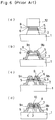
- FIGS 5(a) to 5(c) are diagrams illustrating a high electron mobility transistor (hereinafter referred to as HEMT) formed on an InP substrate included in a prior art semiconductor device, in which figure 5(a) is a top plan view and figures 5(b) and 5(c) are sectional views taken along lines Vb-Vb and Vc-Vc of figure 5(a), respectively.
- HEMT high electron mobility transistor
- a mesa structure comprising compound semiconductor layers, i.e., an intrinsic (hereinafter referred to as i type) InAlAs buffer layer 2, an i type InGaAs channel layer 3, an i type InAlAs spacer layer 4, an n type InAlAs electron supply layer 5, an i type InAlAs Schottky formation layer 6, an n type InAlAs layer 7, and a low-resistance n type InGaAs contact layer 8 with carrier concentration of 2 x 1019 cm3, is disposed on a portion of the InP substrate 1.
- a recess 11 penetrates through the InGaAs contact layer 8 and the InAlAs layer 7 to reach into the Schottky formation layer 6.
- a gate electrode 10 is disposed on the Schottky formation layer 6 exposed on the bottom of the recess 11 and extended onto a portion of the substrate 1.
- Source and drain electrodes 9a and 9b are disposed on the mesa structure where the recess 11 is absent and extended onto portions of the substrate 1.
- the i type InAlAs buffer layer 2 is 1000 ⁇ 1500 angstroms thick and each of the layers disposed on the buffer layer 2 is 100 ⁇ 400 angstroms thick.
- Source and drain regions are formed in the n type InAlAs layer 7.
- Reference numeral 10a designates a bonding pad at an end of the gate electrode 10, to which wires from external devices or devices disposed on other regions of the InP substrate 1 are bonded.
- Figures 6(a) to 6(d) illustrate process steps in a method of producing the HEMT.
- the same reference numerals as in figures 5(a) to 5(c) designate the same or corresponding parts
- reference numeral 12 designates a photoresist pattern.
- the InP substrate 1 the i type InAlAs buffer layer 2, the i type InGaAs channel layer 3, the i type InAlAs spacer layer 4, the n type InAlAs electron supply layer 5, the i type InAlAs Schottky formation layer 6, the n type InAlAs layer 7, and the n type InGaAs contact layer 8, preferably by metal organic chemical vapor deposition (MOCVD).
- MOCVD metal organic chemical vapor deposition
- the semiconductor layers 2 to 8 are etched by wet etching using tartaric acid or the like as an etchant to form the semiconductor layers 2 to 8 in a mesa shape as shown in figure 6(a).
- the mesa-shaped semiconductor layers are isolated from other regions on the InP substrate 1.
- the source and drain electrodes 9a and 9b are formed on prescribed regions on the n type InGaAs contact layer 8, extending onto the surface of the InP substrate 1.
- a bias voltage is applied between the source and drain electrodes 9a and 9b, a two-dimensional gas serving as a channel is formed in the i type InGaAs channel layer 3 in the vicinity of its boundary with the i type InAlAs spacer layer 4, and a current flows through the channel.
- This current is controlled by a voltage applied to the gate electrode 10 to operate the transistor.
- the thickness of the whole compound semiconductor layers must be larger than 0.2 micron.
- the thickness of semiconductor layers between the bottom of the recess, on which the gate electrode is formed, and the surface of the semiconductor substrate must be larger than 0.2 micron.
- a difference in levels between the surface of the semiconductor substrate and the top of the mesa is more than 0.2 micron.
- the HEMT since the HEMT includes the recessed gate, a difference in levels between the surface of the semiconductor substrate and the bottom of the recess is more than 0.2 micron.
- lift-off is usually employed as described above.
- a photoresist film is formed on the mesa and its periphery, and a prescribed portion of the photoresist film is opened by photolithographic technique to form a mask pattern. Then, a metal for the electrode is deposited via the mask pattern, followed by removal of the mask pattern, resulting in an electrode.
- NA a numerical aperture of a projection lens
- ⁇ a wavelength of exposure light
- k1 a constant indicating a lens performance, which is 0.612 in a case of a spherical projection lens according to a theory by Rayleigh. It is known that it is possible to form a fine exposure pattern by increasing the numerical aperture (NA), according to the equation (1).
- a depth of focus is reduced with an increase in the numerical aperture (NA), resulting in an insufficient exposure strength.
- NA numerical aperture
- the gate electrode 10 in forming the gate electrode 10 on the bottom surface of the recess 11 extending onto the surface of the InP substrate 1 by lift-off in the formation of the HEMT, if the opening of the photoresist pattern is fine-patterned in accordance with a desired width of the gate electrode of 0.25 micron or below, the resulting gate electrode is not uniform in its thickness and width and, in some cases, the gate electrode is discontinuous at the edge of the mesa structure, resulting in a HEMT with poor reliability.
- An object of the present invention is to provide a semiconductor device in which a level difference due to a device formed on a substrate is reduced and the device is completely isolated from other regions on the substrate.
- Another object of the present invention is to provide a method for producing the semiconductor device.
- a device in a method of producing a semiconductor device, when a device is formed in a prescribed region of compound semiconductor layers including a low resistance layer which cannot be insulated by ion implantation, upper layers of the compound semiconductor layers including at least the low resistance layer are formed into a mesa shape by etching, and then ion implantation is performed to the compound semiconductor layers other than those beneath the mesa structure, whereby the device is completely isolated from other regions on the semiconductor substrate.
- the device formed on the substrate is isolated from other regions on the substrate using the mesa-etching and the ion implantation, so that a level difference on the substrate due to the device is within a range that does not adversely affect the subsequent process steps, for example, a step of producing electrodes.
- materials and compositions of the compound semiconductor layers isolated by the mesa-etching are selected according to desired device characteristics, without paying consideration on the insulation by ion implantation.
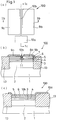
- Figures 1(a) to 1(c) illustrate a HEMT formed on an InP substrate included in a semiconductor device in accordance with a first embodiment of the present invention, in which figure 1(a) is a top plan view and figures 1(b) and 1(c) are sectional views taken along lines Ib-Ib and Ic-Ic of figure 1(a), respectively.
- successively disposed on an InP substrate 1 are an i type InAlAs buffer layer 2, an i type InGaAs channel layer 3, an i type InAlAs spacer layer 4, an n type InAlAs electron supply layer 5, an i type InAlAs Schottky formation layer 6, an n type InAlAs layer 7, and an n type InGaAs contact layer 8a.
- Source and drain electrodes 9a and 9b are disposed on the n type InGaAs contact layer 8a and make an ohmic contact with the contact layer 8a.
- a recess 11 penetrates through the n type InGaAs contact layer 8a and the n type InAlAs layer 7 to reach into the i type InAlAs Schottky formation layer 6.
- a gate electrode 10b having a width of 0.25 micron or below is disposed on the i type InAlAs Schottky formation layer 6 exposed on the bottom surface of the recess 11.
- Reference numeral 13 designates an insulating region for isolating the HEMT 100, which is formed by ion implantation. Source and drain regions are formed in the n type InAlAs layer 7.
- the i type InAsAs buffer layer 2 is 1000 ⁇ 1500 angstroms thick, and each of the layers disposed on the buffer layer 2 is 100 ⁇ 400 angstroms thick.
- the resistance of the n type InGaAs contact layer 8a is reduced by increasing carrier concentration thereof to 1 X 10²⁰/cm3 order, whereby the source and drain electrodes 9a and 9b can favorably make an ohmic contact with the contact layer 8a.
- the contact layer 8a is patterned so that edges of the contact layer are aligned with edges of the insulating region 13.
- FIG. 1 A method of manufacturing the HEMT of figures 1(a) to 1(c) is illustrated in figures 2(a) to 2(d).
- the i type InAlAs buffer layer 2 there are successively grown on on the InP substrate 1, the i type InAlAs buffer layer 2, the i type InGaAs channel layer 3, the i type InAlAs spacer layer 4, the n type InAlAs electron supply layer 5, the i type InAlAs Schottky formation layer 6, the n type InAlAs layer 7, and the n type InGaAs contact layer 8a.
- these layers are grown by MOCVD.
- a photoresist pattern 12 is formed on the n type InGaAs contact layer 8a by a conventional photolithographic technique.
- the n type InGaAs contact layer 8a is selectively etched by wet etching using citric acid as an etchant.
- the n type InGaAs layer 8a which is etched by the wet etching is a layer which cannot be insulated by ion implantation because of its high carrier concentration that provides the low resistance of the layer.
- one of hydrogen (H) ion, boron (B) ion, and iron (Fe) ion, or a combination thereof is used as the ion implanted.
- the source and drain electrodes 9a and 9b comprising Au alloy or Ag alloy that make an ohmic contact with the n type InGaAs contact layer 8a are formed on the contact layer 8a and portions of the insulating region 13 by lift-off, as illustrated in figure 2(c).
- a recess etching is carried out from the surface of the contact layer 8a while measuring a current flowing between the source and drain electrodes 9a and 9b, whereby the thickness of the i type InAlAs Schottky formation layer 6 in a gate region is adjusted to a desired thickness, resulting in the recess 11 shown in figure 2(d).
- the gate electrode 10b having a width of 0.25 micron or below is formed on the Schottky formation layer 6 exposed on the bottom of the recess 11 by lift-off.
- an aperture width of a photoresist pattern used for selectively depositing an electrode metal on the bottom of the recess is 0.25 micron or below.
- a difference in levels between the surface of the insulating region 13 and the surface of the Schottky formation layer 6 exposed on the bottom of the recess 11 is in a range of 200 ⁇ 800 angstroms.
- the pattern exposure is carried out without reducing the resolution and the exposure intensity, whereby a photoresist pattern with a uniform aperture width is obtained.
- the gate electrode 10b having uniform width and thickness is formed with no discontinuity at the edge of the insulating region 13.
- an electrode leading part 10a serving as a bonding pad is formed at an end of the gate electrode 10b. Then, wires from a device formed on the other region on the InP substrate 1 or from an external device are bonded onto the bonding pad 10a.
- the uppermost layer of the HEMT 100 i.e., the low resistance n type InGaAs contact layer 8a is isolated from other regions of the compound semiconductor layers by etching, and then the respective layers beneath the contact layer 8a are isolated by ion implantation, whereby the HEMT 100 is completely isolated on the InP substrate 1.
- the gate electrode 10 having a width of 0.25 micron or below is formed on the i type InAlAs Schottky formation layer 6 exposed on the bottom surface of the recess 11, extending onto the surface of the insulating region 13 by lift-off, the difference in levels between the bottom of the recess and the surface of the insulating region 13 is within a range of 200 to 800 angstroms, resulting in a high dimensional precision of the aperture of the photoresist pattern for forming the electrode, and an electrode with uniform width and thickness is attained, with the result that characteristics of the HEMT are improved.
- the buffer layer 2 may be thicker than 1500 angstroms because the increase in the thickness of the buffer layer 2 does not affect the difference in levels between the bottom surface of the recess 11 and the surface of the insulating region 13. In this case, crystallinities of the semiconductor crystal layers 3 to 8a grown on the buffer layer 2 are improved, with a result that characteristics of the HEMT are further improved.
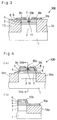
- Figure 3 is a sectional view illustrating a HEMT formed on an InP substrate included in a semiconductor device in accordance with a second embodiment of the present invention.
- the same reference numerals as in figures 1(a) to 1(c) designate the same or corresponding parts.
- width of the n type InGaAs contact layer 8b of the HEMT 300 is narrower than the width of the n type InGaAs contact layer 8a of the HEMT 100 of the first embodiment
- the source and drain electrodes 9a and 9b are disposed over the n type InGaAs contact layer 8a, and intervals between the gate electrode 10b and the source and drain electrodes 9a and 9b are wider than those of the HEMT 100 of the first embodiment.
- a method of manufacturing the HEMT 300 is identical to that of the previously described first embodiment except that photolithography and etching for reducing the width of the n type InGaAs contact layer 8b are carried out before the formation of the source and drain electrodes 9a and 9b.
- the same effects as described in the first embodiment are obtained.
- the width of the n type InGaAs contact layer 8b is narrower and the intervals between the gate electrode 10b and the source and drain electrodes 9a and 9b are wider than those of the HEMT 100 of the first embodiment, a gate junction breakdown voltage is increased, with the result that the characteristics of the HEMT are further improved.
- Figure 4(a) is a sectional view illustrating a HEMT formed on an InP substrate included in a semiconductor device in accordance with a third embodiment of the present invention
- figure 4(b) is a sectional view taken along line IVb-IVb of figure 4(a).
- the same reference numerals as in figures 1(a) to 1(c) designate the same or corresponding parts.
- Reference numeral 13a designates an insulating region formed by ion implantation.
- the semiconductor layers on the i type InAlAs buffer layer 2 are formed in a mesa shape by etching, and a prescribed region 13a of the buffer layer 2 and the InP substrate 1 is insulated by ion implantation, whereby the HEMT 400 is isolated from other regions on the InP substrate 1.
- the gate electrode 10b having a width of 0.25 micron or below is disposed on the bottom surface of the recess 11 and extended onto the surface of the insulating region 13a.
- time for the mesa-etching of the compound semiconductor crystal layers is controlled in the step of figure 6(a) so as to stop the etching on the surface of the i type InAsAs buffer layer 2, and the insulating region 13a is formed by ion implantation. Thereafter, the source and drain electrodes 9a and 9b and the gate electrode 10b are formed to complete the HEMT 400.
- the etching time is controlled so that a level difference on the substrate may not exceed 0.2 micron, differently from the selective etching in the first and second embodiments of the present invention. Therefore, the HEMT 400 which is completely isolated from other regions on the substrate is achieved in a simple process.
- the fine gate electrode 10b achieved in this embodiment has uniform width and continuity at the edge of the mesa structure because the difference in levels between the surface of the insulating region 13a and the bottom surface of the recess 11 is in a range of 400 to 1600 angstroms.
- the HEMT is formed on the InP substrate
- the present invention may be applied to other field effect transistors or other devices formed on semiconductor substrates comprising other materials.
- a device when a device is formed in a prescribed region of compound semiconductor layers including a low resistance layer which cannot be insulated by ion implantation, upper layers of the compound semiconductor layers including at least the low resistance layer are formed into a mesa shape by etching, and ion implantation is carried out into the compound semiconductor layers other than those beneath the mesa structure, whereby the device is completely isolated from other regions on the semiconductor substrate. Therefore, a device structure with a small level difference is attained, resulting in a high-performance device.
- materials and compositions of the compound semiconductor layers isolated by the mesa-etching are selected according to desired device characteristics without paying considerations on the insulation by ion implantation. Therefore, the degree of freedom in selecting materials and compositions of the compound semiconductor layers formed on the semiconductor substrate increases, resulting in a high-performance device.
Landscapes
- Engineering & Computer Science (AREA)
- Power Engineering (AREA)
- Microelectronics & Electronic Packaging (AREA)
- Computer Hardware Design (AREA)
- Physics & Mathematics (AREA)
- Condensed Matter Physics & Semiconductors (AREA)
- General Physics & Mathematics (AREA)
- Ceramic Engineering (AREA)
- Manufacturing & Machinery (AREA)
- Chemical & Material Sciences (AREA)
- Materials Engineering (AREA)
- Junction Field-Effect Transistors (AREA)
- Element Separation (AREA)
Abstract
In a method of producing a semiconductor device, when a device, for example, transistor, is formed in a prescribed region of compound semiconductor layers including a low resistance layer which cannot be insulated by ion implantation, upper layers of the compound semiconductor layers including at least the low resistance layer are formed into a mesa shape by etching, and then ion implantation is performed to the compound semiconductor layers in a region other than the region beneath the mesa structure. Thus, the device formed on the substrate is completely isolated from other regions on the substrate by the mesa-etching and the ion implantation. In the structure thus obtained, a level difference on the substrate due to the device is within a range that does not adversely affect the subsequent process steps, for example, a step of producing electrodes. In addition, materials and compositions of the compound semiconductor layers isolated by the mesa-etching are selected according to desired device characteristics without palying considerations on the insulation by ion implantation. Therefore, a degree of freedom in selecting materials and compositions of the compound semiconductor layers formed on the semiconductor substrate increases, resulting in a high-performance device.
Description
- The present invention relates to a semiconductor device and a production method thereof in which a device is formed in a prescribed region of compound semiconductor layers grown on a semiconductor substrate and, more particularly to a method of isolating the device from other regions on the semiconductor substrate.
- Figures 5(a) to 5(c) are diagrams illustrating a high electron mobility transistor (hereinafter referred to as HEMT) formed on an InP substrate included in a prior art semiconductor device, in which figure 5(a) is a top plan view and figures 5(b) and 5(c) are sectional views taken along lines Vb-Vb and Vc-Vc of figure 5(a), respectively. In these figures, a mesa structure comprising compound semiconductor layers, i.e., an intrinsic (hereinafter referred to as i type)
InAlAs buffer layer 2, an i typeInGaAs channel layer 3, an i typeInAlAs spacer layer 4, an n type InAlAselectron supply layer 5, an i type InAlAsSchottky formation layer 6, an ntype InAlAs layer 7, and a low-resistance n typeInGaAs contact layer 8 with carrier concentration of 2 x 10¹⁹ cm³, is disposed on a portion of theInP substrate 1. Arecess 11 penetrates through the InGaAscontact layer 8 and the InAlAslayer 7 to reach into theSchottky formation layer 6. Agate electrode 10 is disposed on the Schottkyformation layer 6 exposed on the bottom of therecess 11 and extended onto a portion of thesubstrate 1. Source anddrain electrodes recess 11 is absent and extended onto portions of thesubstrate 1. Preferably, the i typeInAlAs buffer layer 2 is 1000 ∼ 1500 angstroms thick and each of the layers disposed on thebuffer layer 2 is 100 ∼ 400 angstroms thick. Source and drain regions are formed in the ntype InAlAs layer 7.Reference numeral 10a designates a bonding pad at an end of thegate electrode 10, to which wires from external devices or devices disposed on other regions of theInP substrate 1 are bonded. - Figures 6(a) to 6(d) illustrate process steps in a method of producing the HEMT. In the figures, the same reference numerals as in figures 5(a) to 5(c) designate the same or corresponding parts, and
reference numeral 12 designates a photoresist pattern. - Initially, there are successively grown on the
InP substrate 1, the i typeInAlAs buffer layer 2, the i typeInGaAs channel layer 3, the i typeInAlAs spacer layer 4, the n type InAlAselectron supply layer 5, the i type InAlAsSchottky formation layer 6, the ntype InAlAs layer 7, and the n typeInGaAs contact layer 8, preferably by metal organic chemical vapor deposition (MOCVD). Then, aphotoresist pattern 12 is formed on the n typeInGaAs contact layer 8 by conventional photolithographic technique. Using thephotoresist pattern 12 as a mask, thesemiconductor layers 2 to 8 are etched by wet etching using tartaric acid or the like as an etchant to form thesemiconductor layers 2 to 8 in a mesa shape as shown in figure 6(a). Thus, the mesa-shaped semiconductor layers are isolated from other regions on theInP substrate 1. Then, as shown in figure 6(b), the source anddrain electrodes InGaAs contact layer 8, extending onto the surface of theInP substrate 1. Then, recess etching is carried out from the surface of thecontact layer 8 while measuring a current flowing between the source anddrain electrodes Schottky formation layer 6 in a gate region is adjusted to a desired thickness, resulting therecess 11 shown in figure 6(c). Thereafter, thegate electrode 10 is formed on the i type InAlAs Schottkyformation layer 6 exposed on the bottom of therecess 11 by lift-off. - In operation, when a bias voltage is applied between the source and
drain electrodes InGaAs channel layer 3 in the vicinity of its boundary with the i typeInAlAs spacer layer 4, and a current flows through the channel. This current is controlled by a voltage applied to thegate electrode 10 to operate the transistor. - In a semiconductor device produced by successively growing compound semiconductor layers on a semiconductor substrate and forming a device in a prescribed region of the compound semiconductor layers, like the above-described semiconductor device in which the HEMT is formed on the InP substrate, the thickness of the whole compound semiconductor layers must be larger than 0.2 micron. In addition, in a field effect transistor having a recessed gate, like the above-described HEMT, the thickness of semiconductor layers between the bottom of the recess, on which the gate electrode is formed, and the surface of the semiconductor substrate must be larger than 0.2 micron.
- Therefore, in a structure as shown in figure 5(b), in which compound semiconductor layers on a semiconductor substrate are formed in a mesa by etching to isolate a device from other regions on the substrate, a difference in levels between the surface of the semiconductor substrate and the top of the mesa is more than 0.2 micron. In figure 5(b), since the HEMT includes the recessed gate, a difference in levels between the surface of the semiconductor substrate and the bottom of the recess is more than 0.2 micron. In this structure, when an electrode is formed on the surface of the mesa or on the bottom of the recess extending onto the surface of the substrate, lift-off is usually employed as described above. More specifically, a photoresist film is formed on the mesa and its periphery, and a prescribed portion of the photoresist film is opened by photolithographic technique to form a mask pattern. Then, a metal for the electrode is deposited via the mask pattern, followed by removal of the mask pattern, resulting in an electrode.
- In forming a photoresist pattern by the above-described photolithographic technique, a reduced projecting exposure apparatus is generally used for exposure process thereof, and a resolution limit R of the reduced projection exposure apparatus is represented as follows:

where NA is a numerical aperture of a projection lens, λ is a wavelength of exposure light, and k1 is a constant indicating a lens performance, which is 0.612 in a case of a spherical projection lens according to a theory by Rayleigh. It is known that it is possible to form a fine exposure pattern by increasing the numerical aperture (NA), according to the equation (1). - In forming a photoresist pattern on a substrate having a level difference of 0.2 micron or more, however, a depth of focus is reduced with an increase in the numerical aperture (NA), resulting in an insufficient exposure strength. This makes it very difficult to project a fine exposure pattern having constant light intensity on the substrate having a level difference of 0.2 micron or more. Therefore, in forming a photoresist pattern having an opening of 0.25 micron or below in width is formed, a uniform width of the opening pattern is not obtained and the width also varies in a depth direction of the opening pattern. In this way, in forming the
gate electrode 10 on the bottom surface of therecess 11 extending onto the surface of theInP substrate 1 by lift-off in the formation of the HEMT, if the opening of the photoresist pattern is fine-patterned in accordance with a desired width of the gate electrode of 0.25 micron or below, the resulting gate electrode is not uniform in its thickness and width and, in some cases, the gate electrode is discontinuous at the edge of the mesa structure, resulting in a HEMT with poor reliability. - It is thought that this problem may be avoided if the device is isolated by implanting ions into regions where the device is not formed until the ions reach the substrate. In the InP system HEMT with the n
type InGaAs layer 8 for contacting with electrodes as an uppermost layer, however, since the n type InGaAs layer is not insulated by ion implantation, the HEMT is not completely. When compositions of the respective compound semiconductor layers are determined so that these layers can be insulated by ion implantation, compositions of the respective layers preferable in view of device characteristics are not obtained. - An object of the present invention is to provide a semiconductor device in which a level difference due to a device formed on a substrate is reduced and the device is completely isolated from other regions on the substrate.
- Another object of the present invention is to provide a method for producing the semiconductor device.
- Other objects and advantages of the present invention will become apparent from the detailed description given hereinafter; it should be understood, however, that the detailed description and specific embodiment are given by way of illustration only, since various changes and modifications within the spirit and scope of the invention will become apparent to those skilled in the art from this detailed description.
- According to an aspect of the present invention, in a method of producing a semiconductor device, when a device is formed in a prescribed region of compound semiconductor layers including a low resistance layer which cannot be insulated by ion implantation, upper layers of the compound semiconductor layers including at least the low resistance layer are formed into a mesa shape by etching, and then ion implantation is performed to the compound semiconductor layers other than those beneath the mesa structure, whereby the device is completely isolated from other regions on the semiconductor substrate. Thus, the device formed on the substrate is isolated from other regions on the substrate using the mesa-etching and the ion implantation, so that a level difference on the substrate due to the device is within a range that does not adversely affect the subsequent process steps, for example, a step of producing electrodes. In addition, materials and compositions of the compound semiconductor layers isolated by the mesa-etching are selected according to desired device characteristics, without paying consideration on the insulation by ion implantation.
-
- Figures 1(a) to 1(c) are diagrams illustrating a HEMT formed on an InP substrate included in a semiconductor device in accordance with a first embodiment of the present invention, in which figure 1(a) is a top plan view and figures 1(b) and 1(c) are sectional views taken along lines Ib-Ib and Ic-Ic of figure 1(a), respectively;
- Figures 2(a) to 2(e) are sectional views illustrating process steps in a method of producing the HEMT of figures 1(a) to 1(c);
- Figure 3 is a sectional view illustrating a HEMT formed on an InP substrate included in a semiconductor device in accordance with a second embodiment of the present invention;
- Figures 4(a) and 4(b) are sectional views illustrating a HEMT formed on an InP substrate included in a semiconductor device in accordance with a third embodiment of the present invention;
- Figures 5(a) to 5(c) are diagrams illustrating a HEMT formed on an InP substrate included in a prior art semiconductor device, in which figure 5(a) is a top plan view and figures 5(b) and 5(c) are sectional views taken along lines Vb-Vb and Vc-Vc of figure 5(a), respectively; and
- Figures 6(a) to 6(d) are sectional views illustrating process steps in a method of producing the HEMT of figures 5(a) to 5(c).
- Figures 1(a) to 1(c) illustrate a HEMT formed on an InP substrate included in a semiconductor device in accordance with a first embodiment of the present invention, in which figure 1(a) is a top plan view and figures 1(b) and 1(c) are sectional views taken along lines Ib-Ib and Ic-Ic of figure 1(a), respectively. In the figures, successively disposed on an
InP substrate 1 are an i typeInAlAs buffer layer 2, an i typeInGaAs channel layer 3, an i typeInAlAs spacer layer 4, an n type InAlAselectron supply layer 5, an i type InAlAsSchottky formation layer 6, an ntype InAlAs layer 7, and an n typeInGaAs contact layer 8a. Source anddrain electrodes InGaAs contact layer 8a and make an ohmic contact with thecontact layer 8a. Arecess 11 penetrates through the n typeInGaAs contact layer 8a and the ntype InAlAs layer 7 to reach into the i type InAlAsSchottky formation layer 6. Agate electrode 10b having a width of 0.25 micron or below is disposed on the i type InAlAsSchottky formation layer 6 exposed on the bottom surface of therecess 11.Reference numeral 13 designates an insulating region for isolating the HEMT 100, which is formed by ion implantation. Source and drain regions are formed in the ntype InAlAs layer 7. In addition, the i typeInAsAs buffer layer 2 is 1000 ∼ 1500 angstroms thick, and each of the layers disposed on thebuffer layer 2 is 100 ∼ 400 angstroms thick. The resistance of the n typeInGaAs contact layer 8a is reduced by increasing carrier concentration thereof to 1 X 10²⁰/cm³ order, whereby the source anddrain electrodes contact layer 8a. Thecontact layer 8a is patterned so that edges of the contact layer are aligned with edges of theinsulating region 13. - A method of manufacturing the HEMT of figures 1(a) to 1(c) is illustrated in figures 2(a) to 2(d).
- Initially, as illustrated in figure 2(a), there are successively grown on on the
InP substrate 1, the i typeInAlAs buffer layer 2, the i typeInGaAs channel layer 3, the i typeInAlAs spacer layer 4, the n type InAlAselectron supply layer 5, the i type InAlAsSchottky formation layer 6, the ntype InAlAs layer 7, and the n typeInGaAs contact layer 8a. Preferably, these layers are grown by MOCVD. Then, aphotoresist pattern 12 is formed on the n typeInGaAs contact layer 8a by a conventional photolithographic technique. Then, using thephotoresist pattern 12 as a mask, the n typeInGaAs contact layer 8a is selectively etched by wet etching using citric acid as an etchant. - Thereafter, an ion implantation is performed using the
photoresist pattern 12 as a mask to form the insulatingregion 13 penetrating through the semiconductor layers 2 to 7 and reaching into theInP substrate 1 as illustrated in figure 2(b). Here, the ntype InGaAs layer 8a which is etched by the wet etching is a layer which cannot be insulated by ion implantation because of its high carrier concentration that provides the low resistance of the layer. Preferably, one of hydrogen (H) ion, boron (B) ion, and iron (Fe) ion, or a combination thereof is used as the ion implanted. - After removing the
photoresist pattern 12, the source anddrain electrodes InGaAs contact layer 8a are formed on thecontact layer 8a and portions of the insulatingregion 13 by lift-off, as illustrated in figure 2(c). - Then, a recess etching is carried out from the surface of the
contact layer 8a while measuring a current flowing between the source anddrain electrodes Schottky formation layer 6 in a gate region is adjusted to a desired thickness, resulting in therecess 11 shown in figure 2(d). - Then, as illustrated in figure 2(e), the
gate electrode 10b having a width of 0.25 micron or below is formed on theSchottky formation layer 6 exposed on the bottom of therecess 11 by lift-off. In the formation of thegate electrode 10b, an aperture width of a photoresist pattern used for selectively depositing an electrode metal on the bottom of the recess is 0.25 micron or below. However, during an exposure process for forming the photoresist pattern, a difference in levels between the surface of the insulatingregion 13 and the surface of theSchottky formation layer 6 exposed on the bottom of therecess 11 is in a range of 200 ∼ 800 angstroms. Therefore, the pattern exposure is carried out without reducing the resolution and the exposure intensity, whereby a photoresist pattern with a uniform aperture width is obtained. As the result, thegate electrode 10b having uniform width and thickness is formed with no discontinuity at the edge of the insulatingregion 13. At the same time, anelectrode leading part 10a serving as a bonding pad is formed at an end of thegate electrode 10b. Then, wires from a device formed on the other region on theInP substrate 1 or from an external device are bonded onto thebonding pad 10a. - In the semiconductor device according to the first embodiment of the present invention, the uppermost layer of the
HEMT 100, i.e., the low resistance n typeInGaAs contact layer 8a is isolated from other regions of the compound semiconductor layers by etching, and then the respective layers beneath thecontact layer 8a are isolated by ion implantation, whereby theHEMT 100 is completely isolated on theInP substrate 1. In addition, when thegate electrode 10 having a width of 0.25 micron or below is formed on the i type InAlAsSchottky formation layer 6 exposed on the bottom surface of therecess 11, extending onto the surface of the insulatingregion 13 by lift-off, the difference in levels between the bottom of the recess and the surface of the insulatingregion 13 is within a range of 200 to 800 angstroms, resulting in a high dimensional precision of the aperture of the photoresist pattern for forming the electrode, and an electrode with uniform width and thickness is attained, with the result that characteristics of the HEMT are improved. - While in the first embodiment the i type
InAlAs buffer layer 2 is 1000 ∼ 1500 angstroms thick, thebuffer layer 2 may be thicker than 1500 angstroms because the increase in the thickness of thebuffer layer 2 does not affect the difference in levels between the bottom surface of therecess 11 and the surface of the insulatingregion 13. In this case, crystallinities of thesemiconductor crystal layers 3 to 8a grown on thebuffer layer 2 are improved, with a result that characteristics of the HEMT are further improved. - Figure 3 is a sectional view illustrating a HEMT formed on an InP substrate included in a semiconductor device in accordance with a second embodiment of the present invention. In figure 3, the same reference numerals as in figures 1(a) to 1(c) designate the same or corresponding parts. In this second embodiment, width of the n type
InGaAs contact layer 8b of theHEMT 300 is narrower than the width of the n typeInGaAs contact layer 8a of theHEMT 100 of the first embodiment, the source anddrain electrodes InGaAs contact layer 8a, and intervals between thegate electrode 10b and the source anddrain electrodes HEMT 100 of the first embodiment. - A method of manufacturing the
HEMT 300 is identical to that of the previously described first embodiment except that photolithography and etching for reducing the width of the n typeInGaAs contact layer 8b are carried out before the formation of the source anddrain electrodes - According to the second embodiment of the present invention, the same effects as described in the first embodiment are obtained. In addition, since the width of the n type
InGaAs contact layer 8b is narrower and the intervals between thegate electrode 10b and the source anddrain electrodes HEMT 100 of the first embodiment, a gate junction breakdown voltage is increased, with the result that the characteristics of the HEMT are further improved. - Figure 4(a) is a sectional view illustrating a HEMT formed on an InP substrate included in a semiconductor device in accordance with a third embodiment of the present invention, and figure 4(b) is a sectional view taken along line IVb-IVb of figure 4(a). In these figures, the same reference numerals as in figures 1(a) to 1(c) designate the same or corresponding parts.
Reference numeral 13a designates an insulating region formed by ion implantation. - In this structure, the semiconductor layers on the i type
InAlAs buffer layer 2 are formed in a mesa shape by etching, and aprescribed region 13a of thebuffer layer 2 and theInP substrate 1 is insulated by ion implantation, whereby theHEMT 400 is isolated from other regions on theInP substrate 1. Thegate electrode 10b having a width of 0.25 micron or below is disposed on the bottom surface of therecess 11 and extended onto the surface of theinsulating region 13a. - In producing the
HEMT 400, time for the mesa-etching of the compound semiconductor crystal layers is controlled in the step of figure 6(a) so as to stop the etching on the surface of the i typeInAsAs buffer layer 2, and theinsulating region 13a is formed by ion implantation. Thereafter, the source anddrain electrodes gate electrode 10b are formed to complete theHEMT 400. - According to the third embodiment of the present invention, in the conventional mesa-etching step of figure 6(a), the etching time is controlled so that a level difference on the substrate may not exceed 0.2 micron, differently from the selective etching in the first and second embodiments of the present invention. Therefore, the
HEMT 400 which is completely isolated from other regions on the substrate is achieved in a simple process. In addition, thefine gate electrode 10b achieved in this embodiment has uniform width and continuity at the edge of the mesa structure because the difference in levels between the surface of theinsulating region 13a and the bottom surface of therecess 11 is in a range of 400 to 1600 angstroms. - While in the above-described first to third embodiments the ion implantation is performed after the mesa-etching of the compound semiconductor layers, this order may be reversed.
- While in the above-described first to third embodiments the HEMT is formed on the InP substrate, the present invention may be applied to other field effect transistors or other devices formed on semiconductor substrates comprising other materials.
- As is evident from the foregoing description, according to the present invention, when a device is formed in a prescribed region of compound semiconductor layers including a low resistance layer which cannot be insulated by ion implantation, upper layers of the compound semiconductor layers including at least the low resistance layer are formed into a mesa shape by etching, and ion implantation is carried out into the compound semiconductor layers other than those beneath the mesa structure, whereby the device is completely isolated from other regions on the semiconductor substrate. Therefore, a device structure with a small level difference is attained, resulting in a high-performance device.
- In addition, according to the present invention, materials and compositions of the compound semiconductor layers isolated by the mesa-etching are selected according to desired device characteristics without paying considerations on the insulation by ion implantation. Therefore, the degree of freedom in selecting materials and compositions of the compound semiconductor layers formed on the semiconductor substrate increases, resulting in a high-performance device.
Claims (13)
- A semiconductor device comprising:
a semiconductor substrate;
compound semiconductor layers disposed on said semiconductor substrate;
a device formed in a prescribed region of said compound semiconductor layers:
upper layers of said compound semiconductor layers being isolated from other regions on said semiconductor substrate by mesa-etching; and
lower layers of said compound semiconductor layers being isolated from other regions on said semiconductor substrate by an insulating region formed around said lower layers by ion implantation. - The semiconductor device of claim 1 wherein said upper layers of said compound semiconductor layers include a low resistance layer which cannot be insulated by ion implantation.
- The semiconductor device of claim 2 wherein a low resistance layer for producing an ohmic contact, which cannot be insulated by ion implantation, is present at the top of the compound semiconductor layers.
- The semiconductor device of claim 3 wherein said low resistance layer is an n type InGaAs layer.
- The semiconductor device of claim 1 wherein a difference in levels between a surface on which an electrode of said device is disposed and the surface of said insulating region on which a portion of said electrode is disposed is below 0.2 micron.
- The semiconductor device of claim 5 wherein said device is a field effect transistor and said electrode is a gate electrode.
- A method of producing a semiconductor device, comprising:
successively growing compound semiconductor layers on a semiconductor substrate;
forming a photoresist pattern with a prescribed width on a region of said compound semiconductor layers where a device is to be formed;
etching said upper layers of said compound semiconductor layers in a mesa shape using said photoresist pattern as a mask; and
insulating a prescribed region of said compound semiconductor layers by ion implantation to isolate the region where the device is to be formed from other regions on the semiconductor substrate. - The method of claim 7 wherein upper layers of said semiconductor layers include a low resistance layer that cannot be insulated by ion implantation.
- The method of claim 8 wherein said low resistance layer that cannot be insulated by ion implantation is a low resistance layer for producing an ohmic contact and disposed at the top of the compound semiconductor layers.
- The method of claim 7 wherein one of hydrogen ion, boron ion, and iron ion, or a combination thereof is used in said ion implantation.
- The method of claim 9 wherein said low resistance layer for ohmic contact is an n type InGaAs layer.
- The method of claim 7 wherein said compound semiconductor layers are etched in a mesa shape so that a difference in levels between a surface on which an electrode of said device is disposed and a surface of said region insulated by ion implantation may be below 0.2 micron.
- The method claim 11 wherein said device is a field effect transistor and said electrode is a gate electrode.
Applications Claiming Priority (2)
| Application Number | Priority Date | Filing Date | Title |
|---|---|---|---|
| JP4236556A JPH0661269A (en) | 1992-08-11 | 1992-08-11 | Semiconductor device and its manufacture |
| JP236556/92 | 1992-08-11 |
Publications (2)
| Publication Number | Publication Date |
|---|---|
| EP0591607A2 true EP0591607A2 (en) | 1994-04-13 |
| EP0591607A3 EP0591607A3 (en) | 1997-01-08 |
Family
ID=17002400
Family Applications (1)
| Application Number | Title | Priority Date | Filing Date |
|---|---|---|---|
| EP93104466A Withdrawn EP0591607A3 (en) | 1992-08-11 | 1993-03-18 | Isolated semiconductor device and production method thereof |
Country Status (3)
| Country | Link |
|---|---|
| US (1) | US5483089A (en) |
| EP (1) | EP0591607A3 (en) |
| JP (1) | JPH0661269A (en) |
Cited By (2)
| Publication number | Priority date | Publication date | Assignee | Title |
|---|---|---|---|---|
| FR2783634A1 (en) * | 1998-09-22 | 2000-03-24 | Koninkl Philips Electronics Nv | METHOD FOR PRODUCING A SEMICONDUCTOR DEVICE INCLUDING STAGES OF ENGRAVING A STACK OF LAYERS BY PHOTOLITHOGRAPHY |
| WO2004020686A2 (en) * | 2002-08-28 | 2004-03-11 | Moxtronics, Inc. | A hybrid beam deposition system and methods for fabricating zno films, p-type zno films, and zno-based ii-vi compound semiconductor devices |
Families Citing this family (4)
| Publication number | Priority date | Publication date | Assignee | Title |
|---|---|---|---|---|
| JP2891244B2 (en) * | 1997-06-16 | 1999-05-17 | 日本電気株式会社 | Field effect transistor |
| JP4822667B2 (en) * | 2004-01-23 | 2011-11-24 | Okiセミコンダクタ株式会社 | Semiconductor device and manufacturing method thereof |
| JP2014007296A (en) * | 2012-06-25 | 2014-01-16 | Advanced Power Device Research Association | Semiconductor device and method for manufacturing the same |
| US10134839B2 (en) * | 2015-05-08 | 2018-11-20 | Raytheon Company | Field effect transistor structure having notched mesa |
Citations (5)
| Publication number | Priority date | Publication date | Assignee | Title |
|---|---|---|---|---|
| EP0283278A2 (en) * | 1987-03-18 | 1988-09-21 | Fujitsu Limited | Compound semiconductor device having nonalloyed ohmic contacts |
| JPH01283943A (en) * | 1988-05-11 | 1989-11-15 | Hitachi Ltd | Compound semiconductor integrated circuit and manufacture thereof |
| JPH01302742A (en) * | 1988-05-30 | 1989-12-06 | Fujitsu Ltd | Compound semiconductor device and manufacture thereof |
| EP0437702A2 (en) * | 1989-11-21 | 1991-07-24 | Fujitsu Limited | Semiconductor integrated circuit of compound semiconductor devices comprising isolation regions and method of making the same |
| JPH04125940A (en) * | 1990-09-17 | 1992-04-27 | Nec Corp | Field effect transistor and manufacture thereof |
Family Cites Families (12)
| Publication number | Priority date | Publication date | Assignee | Title |
|---|---|---|---|---|
| JPS61131526A (en) * | 1984-11-30 | 1986-06-19 | Fujitsu Ltd | Manufacture of semiconductor device |
| US4843033A (en) * | 1985-09-27 | 1989-06-27 | Texas Instruments Incorporated | Method for outdiffusion of zinc into III-V substrates using zinc tungsten silicide as dopant source |
| JPS63104485A (en) * | 1986-10-22 | 1988-05-09 | Hitachi Ltd | Manufacture of semiconductor device |
| US5162877A (en) * | 1987-01-27 | 1992-11-10 | Fujitsu Limited | Semiconductor integrated circuit device and method of producing same |
| US5012318A (en) * | 1988-09-05 | 1991-04-30 | Nec Corporation | Hybrid semiconductor device implemented by combination of heterojunction bipolar transistor and field effect transistor |
| US4935797A (en) * | 1988-10-31 | 1990-06-19 | International Business Machines Corporation | Heterojunction bipolar transistors |
| JPH0366135A (en) * | 1989-08-04 | 1991-03-20 | Fujitsu Ltd | Compound semiconductor device |
| JPH03270155A (en) * | 1990-03-20 | 1991-12-02 | Fujitsu Ltd | Semiconductor device and its manufacture |
| US5014108A (en) * | 1990-05-15 | 1991-05-07 | Harris Corporation | MESFET for dielectrically isolated integrated circuits |
| DE69117866T2 (en) * | 1990-10-26 | 1996-10-10 | Nippon Telegraph & Telephone | Heterojunction field effect transistor |
| US5243207A (en) * | 1991-03-15 | 1993-09-07 | Texas Instruments Incorporated | Method to integrate HBTs and FETs |
| US5166083A (en) * | 1991-03-28 | 1992-11-24 | Texas Instruments Incorporated | Method of integrating heterojunction bipolar transistors with heterojunction FETs and PIN diodes |
-
1992
- 1992-08-11 JP JP4236556A patent/JPH0661269A/en active Pending
-
1993
- 1993-02-25 US US08/022,309 patent/US5483089A/en not_active Expired - Fee Related
- 1993-03-18 EP EP93104466A patent/EP0591607A3/en not_active Withdrawn
Patent Citations (5)
| Publication number | Priority date | Publication date | Assignee | Title |
|---|---|---|---|---|
| EP0283278A2 (en) * | 1987-03-18 | 1988-09-21 | Fujitsu Limited | Compound semiconductor device having nonalloyed ohmic contacts |
| JPH01283943A (en) * | 1988-05-11 | 1989-11-15 | Hitachi Ltd | Compound semiconductor integrated circuit and manufacture thereof |
| JPH01302742A (en) * | 1988-05-30 | 1989-12-06 | Fujitsu Ltd | Compound semiconductor device and manufacture thereof |
| EP0437702A2 (en) * | 1989-11-21 | 1991-07-24 | Fujitsu Limited | Semiconductor integrated circuit of compound semiconductor devices comprising isolation regions and method of making the same |
| JPH04125940A (en) * | 1990-09-17 | 1992-04-27 | Nec Corp | Field effect transistor and manufacture thereof |
Non-Patent Citations (3)
| Title |
|---|
| PATENT ABSTRACTS OF JAPAN vol. 014, no. 065 (E-0884), 6 February 1990 & JP-A-01 283943 (HITACHI LTD), 15 November 1989, * |
| PATENT ABSTRACTS OF JAPAN vol. 014, no. 099 (E-0893), 22 February 1990 & JP-A-01 302742 (FUJITSU LTD), 6 December 1989, * |
| PATENT ABSTRACTS OF JAPAN vol. 016, no. 385 (E-1249), 17 August 1992 & JP-A-04 125940 (NEC CORP), 27 April 1992, * |
Cited By (5)
| Publication number | Priority date | Publication date | Assignee | Title |
|---|---|---|---|---|
| FR2783634A1 (en) * | 1998-09-22 | 2000-03-24 | Koninkl Philips Electronics Nv | METHOD FOR PRODUCING A SEMICONDUCTOR DEVICE INCLUDING STAGES OF ENGRAVING A STACK OF LAYERS BY PHOTOLITHOGRAPHY |
| EP0989602A1 (en) * | 1998-09-22 | 2000-03-29 | Koninklijke Philips Electronics N.V. | Method of manufacturing a semiconductor device using lithography and etching of stacked layers |
| WO2004020686A2 (en) * | 2002-08-28 | 2004-03-11 | Moxtronics, Inc. | A hybrid beam deposition system and methods for fabricating zno films, p-type zno films, and zno-based ii-vi compound semiconductor devices |
| WO2004020686A3 (en) * | 2002-08-28 | 2004-10-14 | Moxtronics Inc | A hybrid beam deposition system and methods for fabricating zno films, p-type zno films, and zno-based ii-vi compound semiconductor devices |
| US7824955B2 (en) | 2002-08-28 | 2010-11-02 | Moxtronics, Inc. | Hybrid beam deposition system and methods for fabricating metal oxide-ZnO films, p-type ZnO films, and ZnO-based II-VI compound semiconductor devices |
Also Published As
| Publication number | Publication date |
|---|---|
| EP0591607A3 (en) | 1997-01-08 |
| US5483089A (en) | 1996-01-09 |
| JPH0661269A (en) | 1994-03-04 |
Similar Documents
| Publication | Publication Date | Title |
|---|---|---|
| US5510280A (en) | Method of making an asymmetrical MESFET having a single sidewall spacer | |
| US4213840A (en) | Low-resistance, fine-line semiconductor device and the method for its manufacture | |
| US5362677A (en) | Method for producing a field effect transistor with a gate recess structure | |
| KR20050051650A (en) | Method of forming a self-aligned, selectively etched, double recess high electron mobility transistor | |
| US3951708A (en) | Method of manufacturing a semiconductor device | |
| EP0810645B1 (en) | Method of fabricating double photoresist layer self-aligned heterojunction bipolar transistor | |
| EP0305975A2 (en) | Compound semiconductor MESFET | |
| EP0591607A2 (en) | Isolated semiconductor device and production method thereof | |
| EP0436192B1 (en) | Method of Manufacturing Semiconductor Device with Taper Structure | |
| US6656802B2 (en) | Process of manufacturing a semiconductor device including a buried channel field effect transistor | |
| US20030173584A1 (en) | Semiconductor integrated circuit device and method of fabricating the same | |
| US4587540A (en) | Vertical MESFET with mesa step defining gate length | |
| JPH1140578A (en) | Semiconductor device and its manufacture | |
| CA1271850A (en) | Method for fabricating a field-effect transistor with a self-aligned gate | |
| US20030113985A1 (en) | Field effect transistor semiconductor and method for manufacturing the same | |
| EP0091548B1 (en) | Semiconductor structure comprising a mesa region, process for forming a semiconductor mesa; vertical field effect transistor and method of forming a vertical semiconductor device | |
| US5652451A (en) | Recessed gate field effect transistor | |
| KR100232152B1 (en) | Manufacturing method of mesfet | |
| US6291277B1 (en) | Method of manufacturing a semiconductor device including etching of a stack of layers by means of photolithography | |
| EP0146212A1 (en) | Schottky barrier diode and method of manufacturing it | |
| JP2002009275A (en) | Field effect compound semiconductor device | |
| JPH0797634B2 (en) | Field effect transistor and manufacturing method thereof | |
| JPS61137371A (en) | Manufacture of semiconductor device | |
| JPS59130481A (en) | Schottky gate field effect transistor | |
| JPH0247869A (en) | Method of forming electrode of semiconductor device |
Legal Events
| Date | Code | Title | Description |
|---|---|---|---|
| PUAI | Public reference made under article 153(3) epc to a published international application that has entered the european phase |
Free format text: ORIGINAL CODE: 0009012 |
|
| AK | Designated contracting states |
Kind code of ref document: A2 Designated state(s): DE FR GB |
|
| PUAL | Search report despatched |
Free format text: ORIGINAL CODE: 0009013 |
|
| AK | Designated contracting states |
Kind code of ref document: A3 Designated state(s): DE FR GB |
|
| 17P | Request for examination filed |
Effective date: 19970324 |
|
| STAA | Information on the status of an ep patent application or granted ep patent |
Free format text: STATUS: THE APPLICATION IS DEEMED TO BE WITHDRAWN |
|
| 18D | Application deemed to be withdrawn |
Effective date: 19981001 |