EP0589727A2 - Semiconductor laser device - Google Patents
Semiconductor laser device Download PDFInfo
- Publication number
- EP0589727A2 EP0589727A2 EP93307608A EP93307608A EP0589727A2 EP 0589727 A2 EP0589727 A2 EP 0589727A2 EP 93307608 A EP93307608 A EP 93307608A EP 93307608 A EP93307608 A EP 93307608A EP 0589727 A2 EP0589727 A2 EP 0589727A2
- Authority
- EP
- European Patent Office
- Prior art keywords
- semiconductor laser
- active layer
- current
- laser device
- layer
- Prior art date
- Legal status (The legal status is an assumption and is not a legal conclusion. Google has not performed a legal analysis and makes no representation as to the accuracy of the status listed.)
- Granted
Links
Images


Classifications
-
- H—ELECTRICITY
- H01—ELECTRIC ELEMENTS
- H01S—DEVICES USING THE PROCESS OF LIGHT AMPLIFICATION BY STIMULATED EMISSION OF RADIATION [LASER] TO AMPLIFY OR GENERATE LIGHT; DEVICES USING STIMULATED EMISSION OF ELECTROMAGNETIC RADIATION IN WAVE RANGES OTHER THAN OPTICAL
- H01S5/00—Semiconductor lasers
- H01S5/10—Construction or shape of the optical resonator, e.g. extended or external cavity, coupled cavities, bent-guide, varying width, thickness or composition of the active region
- H01S5/16—Window-type lasers, i.e. with a region of non-absorbing material between the active region and the reflecting surface
-
- H—ELECTRICITY
- H01—ELECTRIC ELEMENTS
- H01S—DEVICES USING THE PROCESS OF LIGHT AMPLIFICATION BY STIMULATED EMISSION OF RADIATION [LASER] TO AMPLIFY OR GENERATE LIGHT; DEVICES USING STIMULATED EMISSION OF ELECTROMAGNETIC RADIATION IN WAVE RANGES OTHER THAN OPTICAL
- H01S5/00—Semiconductor lasers
- H01S5/04—Processes or apparatus for excitation, e.g. pumping, e.g. by electron beams
- H01S5/042—Electrical excitation ; Circuits therefor
- H01S5/0425—Electrodes, e.g. characterised by the structure
- H01S5/04254—Electrodes, e.g. characterised by the structure characterised by the shape
-
- H—ELECTRICITY
- H01—ELECTRIC ELEMENTS
- H01S—DEVICES USING THE PROCESS OF LIGHT AMPLIFICATION BY STIMULATED EMISSION OF RADIATION [LASER] TO AMPLIFY OR GENERATE LIGHT; DEVICES USING STIMULATED EMISSION OF ELECTROMAGNETIC RADIATION IN WAVE RANGES OTHER THAN OPTICAL
- H01S5/00—Semiconductor lasers
- H01S5/10—Construction or shape of the optical resonator, e.g. extended or external cavity, coupled cavities, bent-guide, varying width, thickness or composition of the active region
- H01S5/16—Window-type lasers, i.e. with a region of non-absorbing material between the active region and the reflecting surface
- H01S5/168—Window-type lasers, i.e. with a region of non-absorbing material between the active region and the reflecting surface with window regions comprising current blocking layers
-
- H—ELECTRICITY
- H01—ELECTRIC ELEMENTS
- H01S—DEVICES USING THE PROCESS OF LIGHT AMPLIFICATION BY STIMULATED EMISSION OF RADIATION [LASER] TO AMPLIFY OR GENERATE LIGHT; DEVICES USING STIMULATED EMISSION OF ELECTROMAGNETIC RADIATION IN WAVE RANGES OTHER THAN OPTICAL
- H01S5/00—Semiconductor lasers
- H01S5/20—Structure or shape of the semiconductor body to guide the optical wave ; Confining structures perpendicular to the optical axis, e.g. index or gain guiding, stripe geometry, broad area lasers, gain tailoring, transverse or lateral reflectors, special cladding structures, MQW barrier reflection layers
- H01S5/22—Structure or shape of the semiconductor body to guide the optical wave ; Confining structures perpendicular to the optical axis, e.g. index or gain guiding, stripe geometry, broad area lasers, gain tailoring, transverse or lateral reflectors, special cladding structures, MQW barrier reflection layers having a ridge or stripe structure
- H01S5/223—Buried stripe structure
- H01S5/2231—Buried stripe structure with inner confining structure only between the active layer and the upper electrode
-
- H—ELECTRICITY
- H01—ELECTRIC ELEMENTS
- H01S—DEVICES USING THE PROCESS OF LIGHT AMPLIFICATION BY STIMULATED EMISSION OF RADIATION [LASER] TO AMPLIFY OR GENERATE LIGHT; DEVICES USING STIMULATED EMISSION OF ELECTROMAGNETIC RADIATION IN WAVE RANGES OTHER THAN OPTICAL
- H01S5/00—Semiconductor lasers
- H01S5/30—Structure or shape of the active region; Materials used for the active region
- H01S5/32—Structure or shape of the active region; Materials used for the active region comprising PN junctions, e.g. hetero- or double- heterostructures
- H01S5/3211—Structure or shape of the active region; Materials used for the active region comprising PN junctions, e.g. hetero- or double- heterostructures characterised by special cladding layers, e.g. details on band-discontinuities
-
- H—ELECTRICITY
- H01—ELECTRIC ELEMENTS
- H01S—DEVICES USING THE PROCESS OF LIGHT AMPLIFICATION BY STIMULATED EMISSION OF RADIATION [LASER] TO AMPLIFY OR GENERATE LIGHT; DEVICES USING STIMULATED EMISSION OF ELECTROMAGNETIC RADIATION IN WAVE RANGES OTHER THAN OPTICAL
- H01S5/00—Semiconductor lasers
- H01S5/30—Structure or shape of the active region; Materials used for the active region
- H01S5/32—Structure or shape of the active region; Materials used for the active region comprising PN junctions, e.g. hetero- or double- heterostructures
- H01S5/323—Structure or shape of the active region; Materials used for the active region comprising PN junctions, e.g. hetero- or double- heterostructures in AIIIBV compounds, e.g. AlGaAs-laser, InP-based laser
- H01S5/32308—Structure or shape of the active region; Materials used for the active region comprising PN junctions, e.g. hetero- or double- heterostructures in AIIIBV compounds, e.g. AlGaAs-laser, InP-based laser emitting light at a wavelength less than 900 nm
Definitions
- This invention relates to a semiconductor laser device to be suitably used for a telecommunications or optical application as it is driven with an enhanced energy output level.
- a proposed solution for these problems is the provision of a structure (window structure) that effectively prevents the phenomenon of light absorption from occurring on the facets of a semiconductor laser.
- such a structure comprises part of an active layer that can effectively expand a band gap and hence suppress light absorption and optical damage of the part of the semiconductor laser device caused by light absorption.
- the semiconductor laser device can also be degraded as the surface recombination current running on the device increases as a result of an electric current given rise to by a bias voltage applied to the facets of the device having a band gap expanding area and the Joule's heat generated by the current.
- an object of the invention to provide a semiconductor laser that can be driven for a high-output power level without degradation in the quality of the device.
- a semiconductor laser device comprising double heterostructure including an active layer and an electrode layer arranged on a semiconductor substrate and having a current injection region extending through the electrode layer and the active layer, a structural scheme being provided either in a region located above the active layer or in a region covering an resonator of the active layer in order to reduce the injection current level of the device.
- the structural scheme provided in a semiconductor laser device according to the invention in order to reduce the injection current level of the device is preferably selected from the three alternatives, mentioned below.
- a first alternative is a Schottky junction of a metal and a semiconductor having a relatively high threshold voltage and arranged in the current injection region and close to a light reflecting facet of the region.
- a second one is an insulating object arranged between the electrode layer and the active layer and close to a light reflecting facet of the current injection region.
- a third alternative is a semiconductor region having a band gap greater than that of the active layer and arranged on the resonator side of the active layer and a current noninjection structure is formed on the resonator side of the active layer, including the semiconductor region.
- Such a current noninjection structure may comprise a pnp-type current blocking layer. It may alternatively comprise an npn-type current blocking layer. Still alternatively, it may comprise a layer with no electrode.
- the injection current density of that area can be made lower than that of the remaining area of the device.
- any significant temperature rise on the light reflecting facets (in the current injection region) can be effectively prevented from occurring during current injection so that no reduction of the band gap of the device and consequent light absorption will take place.
- optical output characteristics of a semiconductor laser device are remarkably improved to greatly enhance the reliability of the device when the rate of generation of Joule's heat is suppressed in the particular area of the device in a manner as described above.
- the current non-injection structure being composed of a pnp-type current blocking layer, an npn-type current blocking layer or a layer with no electrode.
- Fig. 1 is a schematic front view of a first embodiment of semiconductor laser device of the invention.
- Fig. 2 is a schematic partial sectional view of the first embodiment cut along A-A line in Fig. 1.
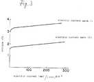
- Fig. 3 is a graph showing the relationship between the electric current and the voltage at the two opposite ends of the ridge mesa and a similar relationship observed between two different points of the ridge mesa of the first embodiment of Fig. 1.
- Fig. 4 is a schematic front view of a second embodiment of semiconductor laser device of the invention.
- Fig. 5 is a schematic partial sectional view of the second embodiment cut along B-B line in Fig. 4.
- Figs. 1 and 2 show a first embodiment of semiconductor laser device of the invention.
- the device comprises an n-GaAs substrate 1, an n-GaAs buffer layer 2, an n-InGaP lower clad layer 3, an n-GaAs lower light confinement layer 4, a p-In 0. 2 Ga 0. 8 As active layer 5, a p GaAs upper light confinement layer 6, a p-InGaP upper clad layer 7, a p+ GaAs cap layer 8, a p-electrode layer 9, an n-electrode layer 10 and a polyimide layer 11.
- a semiconductor laser device as illustrated in Figs. 1 and 2 may typically be prepared in a manner as described below.
- a ridge mesa is formed to a ridge width of 2 ⁇ m and a cavity length of 800 ⁇ m on the n-GaAs substrate 1 in a mesa formation process using a photolithography technique.
- a narrow etching mask is laid on the upper surface of the ridge mesa and then the cap layer 8 is removed except the masked area by photolithography.
- the etching mask is 740 ⁇ m long and covers a middle portion of the ridge mesa having a length of 800 ⁇ m, the latter is etched at the opposite end sections by 30 ⁇ m on the light reflecting facet side.
- the etched opposite end sections of the ridge mesa are filled with a polyimide layer 11 and then a Ti/Pt/Au p-electrode layer 9 and a metal n-electrode layer 10 are fitted respectively to the epitaxially grown side and the lower surface of the n-GaAs substrate 1 to produce a complete ridge waveguide type semiconductor laser device.
- a Schottky junction is formed by InGaP doped to a low concentration level and Ti as described above.
- an excellent ohmic junction is formed by GaAs doped to a high concentration level and Ti.
- Example 1 the embodiment (hereinafter referred to as Example 1) will show a relatively low injection current level at the opposite ends of the ridge mesa when it is driven for laser emission.
- Comparison Example 1 an unconfined current injection type semiconductor laser device having a ridge mesa with unetched opposite ends was prepared in a manner similar to that of preparing Example 1 (hereinafter referred to as Comparison Example 1).
- the destruction optical output 400mW
- the increase rate of the threshold ciirrent 1%
- the destruction optical output 300mW
- the increase rate of the threshold current 5%
- Example 1 showed a destruction optical output greater than that of Comparison Example 1 although the increase rate of the threshold current of Example 1 was not significantly lower than that of Comparison Example 1.
- the destruction optical output and the increase rate of the threshold current of a substitute embodiment obtained by arranging an insulating object between the electrode layer and the active layer and close to a light reflecting facet of the current injection region showed similar results.
- Figs. 4 and 5 show a second embodiment of semiconductor laser device of the invention.
- the device comprises an n-GaAs substrate 21, an n-GaAs buffer layer 22, an n-InGaP lower clad layer 23, an n-GaAs lower light confinement layer 24, a p-In 0. 2 Ga 0. 8 As active layer 25, a p-GaAs upper light confinement layer 26, a p-InGaP upper clad layer 27, a p+-GaAs cap layer 28, a p-electrode layer 29, an n-electrode layer 30, a polyimide layer 11 and a pair of Zn diffusion regions 31.
- a semiconductor laser device as illustrated in Figs. 4 and 5 may typically be prepared in a manner as described below.
- a p-GaAs upper light confinement layer 26 with a thickness of 0.03 ⁇ m and n 3x1017cm ⁇ 3
- a ridge mesa is formed to a ridge width of 3 ⁇ m and a cavity length of 800 ⁇ m on the n-GaAs substrate 1 in a mesa formation process using a photolithography technique.
- a narrow etching mask is laid on the upper surface of the ridge mesa and zinc is caused to diffuse into the unmasked regions of the ridge mesa to form a pair of Zn diffusion regions 32 arranged at the respective opposite ends of the ridge mesa also by using a photolithography technique.
- each of the Zn diffusion regions 32 has a length of 20 ⁇ m as shown in Fig. 5.
- the portions of the active layer that are composed of a quantum well layer are caused to show disordering. Then, the band gap of the disordering of the active layer 25 will be expanded relative to that of the remaining portions to show a so-called window structure.
- the etching mask is 740 ⁇ m long and covers a middle portion of the ridge mesa having a length of 800 ⁇ m, the latter is etched at the opposite end sections by 30 ⁇ m on the light reflecting facet side as shown in Fig. 5.
- the etched opposite end sections of the ridge mesa are filled with a polyimide layer 31 to form a current noninjection structure.
- a Ti/Pt/Au p-electrode layer 29 and a metal n-electrode layer 30 are fitted, respectively to the epitaxially grown side and the lower surface of the n-GaAs substrate 1 to produce a complete ridge waveguide type semiconductor laser device.
- Example 2 has a cavity length of 800 ⁇ m and the portions of the active layer 25 located at the opposite ends and each having a length of 20 ⁇ m show a window structure where the band gap is greater than that of the remaining portions of the active layer 25, while each of the opposite end portions of the ridge mesa presents a current noninjection structure for a length of 30 ⁇ m.
- Comparison Example 2 a semiconductor laser device provided with a window structure but devoid of a current noninjection structure (hereinafter referred to as Comparison Example 2) and a semiconductor laser device having neither a window structure nor a current noninjection structure (hereinafter referred to as Comparison Example 3) were prepared in a manner similar to that of preparing Example 2.
- the destruction optical output 500mW
- the increase rate of the threshold current ⁇ 0.5%
- the destruction optical output 400mW
- the increase rate of the threshold current 1%
- the destruction optical output 300mW
- the increase rate of the threshold current 5%
- Example 2 showed a destruction optical output greater than those of Comparison Examples 2 and 3 although the increase rate of the threshold current of Example 2 was not significantly lower than those of Comparison Examples 2 and 3.
- the semiconductor laser device of Example 2 has both a window structure and a current noninjection structure that can effectively suppress the degradation of the laser emitting surface of the device.
- the destruction optical output and the increase rate of the threshold current of a substitute embodiment obtained by arranging a pnp or npn current blocking layer for the current noninjection structure and another substitute embodiment obtained by arranging a void electrode section for the current noninjection structure showed similar improvements.
- a semiconductor laser device comprises a double heterostructure including an active layer and an electrode layer arranged on a semiconductor substrate and has a current injection region extending through the electrode layer and the active layer. Additionally, a structural scheme is provided either in a region located above the active layer or in a region covering an resonator of the active layer in order to reduce the injection current level of the device. With such an arrangement, the output power level of the semiconductor laser device is remarkably enhanced and its reliability is greatly improved.
- a semiconductor laser device provided with a structural scheme in a region covering the resonator of the active layer of the device is particularly advantageous as such a device can be prepared easily and economically.
Abstract
Description
- This invention relates to a semiconductor laser device to be suitably used for a telecommunications or optical application as it is driven with an enhanced energy output level.
- There has been an increasing demand for GaAs-type semiconductor laser devices capable of being driven with a high energy output level for telecommunications and optical applications.
- When a semiconductor laser device is driven to show a high-output power level, there arise problems including catastrophic optical damage at the facets of laser and corrosion, when the device is used continuously for a long period of time.
- It is believed that these problems take place when the temperature of the facets of a semiconductor laser device is subjected to a repetition of the cycle of rise in the surface temperature, reduction in the band gap, light absorption and increase in the surface recombination current.
- A proposed solution for these problems is the provision of a structure (window structure) that effectively prevents the phenomenon of light absorption from occurring on the facets of a semiconductor laser.
- More specifically, such a structure comprises part of an active layer that can effectively expand a band gap and hence suppress light absorption and optical damage of the part of the semiconductor laser device caused by light absorption.
- With such a preventive measure as described above, however, the semiconductor laser device can also be degraded as the surface recombination current running on the device increases as a result of an electric current given rise to by a bias voltage applied to the facets of the device having a band gap expanding area and the Joule's heat generated by the current.
- In view of the above technological problems, it is, therefore, an object of the invention to provide a semiconductor laser that can be driven for a high-output power level without degradation in the quality of the device.
- According to the invention, the above object and other objects of the invention are achieved by providing a semiconductor laser device comprising double heterostructure including an active layer and an electrode layer arranged on a semiconductor substrate and having a current injection region extending through the electrode layer and the active layer, a structural scheme being provided either in a region located above the active layer or in a region covering an resonator of the active layer in order to reduce the injection current level of the device.
- The structural scheme provided in a semiconductor laser device according to the invention in order to reduce the injection current level of the device is preferably selected from the three alternatives, mentioned below.
- A first alternative is a Schottky junction of a metal and a semiconductor having a relatively high threshold voltage and arranged in the current injection region and close to a light reflecting facet of the region.
- A second one is an insulating object arranged between the electrode layer and the active layer and close to a light reflecting facet of the current injection region.
- A third alternative is a semiconductor region having a band gap greater than that of the active layer and arranged on the resonator side of the active layer and a current noninjection structure is formed on the resonator side of the active layer, including the semiconductor region.
- Such a current noninjection structure may comprise a pnp-type current blocking layer. It may alternatively comprise an npn-type current blocking layer. Still alternatively, it may comprise a layer with no electrode.
- When a Schottky junction is formed closed to a light reflecting facet of the current injection region of a semiconductor laser device according to the invention as in the case of the first embodiment, which will be described hereinafter, the injection current density of that area can be made lower than that of the remaining area of the device.
- By so reducing the injection current density of a particular area, any significant temperature rise on the light reflecting facets (in the current injection region) can be effectively prevented from occurring during current injection so that no reduction of the band gap of the device and consequent light absorption will take place.
- It should be noted that such an arrangement can be easily realized in manufacturing semiconductor laser devices of the type under consideration.
- The effects as described above for the first embodiment can also be achieved when, alternatively, an insulating object is arranged between the electrode layer and the active layer of a semiconductor laser device according to the invention as in the case of the second embodiment.
- Again, no temperature rise is observed on the resonator facet and in its vicinity and, therefore, the injection current in those areas is reduced when, still alternatively, a semiconductor region having a band gap greater than that of the active layer and arranged on the resonator side of the active layer and a current noninjection structure is formed on the resonator side of the active layer, including the semiconductor region, as in the case of the third embodiment.
- The optical output characteristics of a semiconductor laser device are remarkably improved to greatly enhance the reliability of the device when the rate of generation of Joule's heat is suppressed in the particular area of the device in a manner as described above.
- The above statement holds true, regardless of the current non-injection structure being composed of a pnp-type current blocking layer, an npn-type current blocking layer or a layer with no electrode.
- Now, the present invention will be described by referring to the accompanying drawings that illustrate preferred embodiments of the invention.
- Fig. 1 is a schematic front view of a first embodiment of semiconductor laser device of the invention.
- Fig. 2 is a schematic partial sectional view of the first embodiment cut along A-A line in Fig. 1.
- Fig. 3 is a graph showing the relationship between the electric current and the voltage at the two opposite ends of the ridge mesa and a similar relationship observed between two different points of the ridge mesa of the first embodiment of Fig. 1.
- Fig. 4 is a schematic front view of a second embodiment of semiconductor laser device of the invention.
- Fig. 5 is a schematic partial sectional view of the second embodiment cut along B-B line in Fig. 4.
- Figs. 1 and 2 show a first embodiment of semiconductor laser device of the invention.
- Referring to Figs. 1 and 2, the device comprises an n-
GaAs substrate 1, an n-GaAs buffer layer 2, an n-InGaPlower clad layer 3, an n-GaAs lowerlight confinement layer 4, a p-In0. 2Ga0. 8Asactive layer 5, a p GaAs upper light confinement layer 6, a p-InGaPupper clad layer 7, a p⁺GaAs cap layer 8, a p-electrode layer 9, an n-electrode layer 10 and apolyimide layer 11. - A semiconductor laser device as illustrated in Figs. 1 and 2 may typically be prepared in a manner as described below.
- Firstly, an n-
GaAs buffer layer 2 with a thickness of 0.5µm and n=1x10¹⁸cm⁻³, an n-InGaPlower clad layer 3 with a thickness of 1.2µm and n=1x10¹⁸cm⁻³, an n-GaAs lowerlight confining layer 4 with a thickness of 0.03µm and n=3x10¹⁷cm⁻³, a p-In0. 2Ga0. 8Asactive layer 5 with a thickness of 80Ȧ and n=3x10¹⁷cm⁻³, a p-GaAs upper light confining layer 6 with a thickness of 0.03µm and n=3x10¹⁷cm⁻³, a p-InGaPupper clad layer 7 with a thickness of 1.0µm and n=1x10¹⁸cm⁻³ and a p⁺-GaAs cap layer 8 with a thickness of 0.5µm and n=4x10¹⁹cm⁻³ are sequentially formed on an n-GaAs substrate 1 in a crystal growth process using an epitaxial growth technique. - Thereafter, a ridge mesa is formed to a ridge width of 2µm and a cavity length of 800µm on the n-
GaAs substrate 1 in a mesa formation process using a photolithography technique. - Subsequently, a narrow etching mask is laid on the upper surface of the ridge mesa and then the
cap layer 8 is removed except the masked area by photolithography. - Since the etching mask is 740µm long and covers a middle portion of the ridge mesa having a length of 800µm, the latter is etched at the opposite end sections by 30µm on the light reflecting facet side.
- Finally, the etched opposite end sections of the ridge mesa are filled with a
polyimide layer 11 and then a Ti/Pt/Au p-electrode layer 9 and a metal n-electrode layer 10 are fitted respectively to the epitaxially grown side and the lower surface of the n-GaAs substrate 1 to produce a complete ridge waveguide type semiconductor laser device. - Note that, in the above embodiment, the titanium (Ti) constituting part of the p-
electrode plate 9 is held in contact with the p-InGaP (p-1x10¹⁸cm⁻³)upper clad layer 7 at the opposite end sections of the ridge mesa while all the remaining surface areas of the titanium of theplate 9 is held in contact with the p⁺-GaAs(n=4x10¹⁹cm⁻³)cap layer 8. - In an experiment conducted by using the above embodiment of semiconductor laser device, the current-voltage relationship was determined between the p-
electrode 9 and thecap layer 8 and between the p-electrode 9 and theupper clad layer 7 by means of a known method of measurement. The results are illustrated in Fig. 3. - Referring to Fig. 3, it will be understood that the voltage is higher between the opposite ends of the ridge mesa (electric current path (1)) than between any two other points of the ridge mesa (electric current path (2)).
- The reason for this is that a Schottky junction is formed by InGaP doped to a low concentration level and Ti as described above.
- Incidentally, it should be noted that an excellent ohmic junction is formed by GaAs doped to a high concentration level and Ti.
- Therefore, the embodiment (hereinafter referred to as Example 1) will show a relatively low injection current level at the opposite ends of the ridge mesa when it is driven for laser emission.
- For the purpose of comparison, an unconfined current injection type semiconductor laser device having a ridge mesa with unetched opposite ends was prepared in a manner similar to that of preparing Example 1 (hereinafter referred to as Comparison Example 1).
- Then, the destruction optical output at which the laser emitting surface comes to be destroyed due to temperature rise and the increase rate of the threshold current when driven at 50°C and 100mW for 1,000 hours were determined for both Example 1 and Comparison Example 1, as listed below.
- the destruction optical output: 400mW
the increase rate of the threshold ciirrent: 1% - the destruction optical output: 300mW
the increase rate of the threshold current: 5% - Clearly, Example 1 showed a destruction optical output greater than that of Comparison Example 1 although the increase rate of the threshold current of Example 1 was not significantly lower than that of Comparison Example 1.
- The destruction optical output and the increase rate of the threshold current of a substitute embodiment obtained by arranging an insulating object between the electrode layer and the active layer and close to a light reflecting facet of the current injection region showed similar results.
- Now, a second embodiment of the invention will be described by referring to Figs. 4 and 5.
- Figs. 4 and 5 show a second embodiment of semiconductor laser device of the invention.
- Referring to Figs. 4 and 6, the device comprises an n-
GaAs substrate 21, an n-GaAs buffer layer 22, an n-InGaPlower clad layer 23, an n-GaAs lowerlight confinement layer 24, a p-In0. 2Ga0. 8Asactive layer 25, a p-GaAs upperlight confinement layer 26, a p-InGaPupper clad layer 27, a p⁺-GaAs cap layer 28, a p-electrode layer 29, an n-electrode layer 30, apolyimide layer 11 and a pair ofZn diffusion regions 31. - A semiconductor laser device as illustrated in Figs. 4 and 5 may typically be prepared in a manner as described below.
- Firstly, an n-
GaAs buffer layer 22 with a thickness of 0.5µm and n=1x10¹⁸cm⁻³, an n-InGaP lower cladlayer 23 with a thickness of 1.2µm and n=1x10¹⁸cm⁻³, an n-GaAs lowerlight confinement layer 24 with a thickness of 0.03µm and n=3x10¹⁷cm⁻³, a p-In0. 2Ga0. 8Asactive layer 25 with a thickness of 80Ȧ and n=3x10¹⁷cm⁻³, a p-GaAs upperlight confinement layer 26 with a thickness of 0.03µm and n=3x10¹⁷cm⁻³, a p-InGaP upper cladlayer 27 with a thickness of 1.0µm and n=1x10¹⁸cm⁻³ and a p⁺-GaAs cap layer 28 with a thickness of 0.5µm and n=4x10¹⁹cm⁻³ are sequentially formed on an n-GaAs substrate 1 in a crystal growth process using an epitaxial growth technique. - Thereafter, a ridge mesa is formed to a ridge width of 3µm and a cavity length of 800µm on the n-
GaAs substrate 1 in a mesa formation process using a photolithography technique. - Subsequently, a narrow etching mask is laid on the upper surface of the ridge mesa and zinc is caused to diffuse into the unmasked regions of the ridge mesa to form a pair of
Zn diffusion regions 32 arranged at the respective opposite ends of the ridge mesa also by using a photolithography technique. - Since the etching mask is 760µm long and covers a middle portion of the ridge mesa having a length of 800µm, each of the
Zn diffusion regions 32 has a length of 20µm as shown in Fig. 5. - As the
Zn diffusion regions 32 are formed, the portions of the active layer that are composed of a quantum well layer are caused to show disordering. Then, the band gap of the disordering of theactive layer 25 will be expanded relative to that of the remaining portions to show a so-called window structure. - Then, another narrow etching mask is laid on the upper surface of the ridge mesa and the
cap layer 28 is removed except the masked area again by photolithography. - Since the etching mask is 740µm long and covers a middle portion of the ridge mesa having a length of 800µm, the latter is etched at the opposite end sections by 30µm on the light reflecting facet side as shown in Fig. 5.
- Thereafter, the etched opposite end sections of the ridge mesa are filled with a
polyimide layer 31 to form a current noninjection structure. - Finally, a Ti/Pt/Au p-
electrode layer 29 and a metal n-electrode layer 30 are fitted, respectively to the epitaxially grown side and the lower surface of the n-GaAs substrate 1 to produce a complete ridge waveguide type semiconductor laser device. - Note that the above embodiment (hereinafter referred to as Example 2) has a cavity length of 800µm and the portions of the
active layer 25 located at the opposite ends and each having a length of 20µm show a window structure where the band gap is greater than that of the remaining portions of theactive layer 25, while each of the opposite end portions of the ridge mesa presents a current noninjection structure for a length of 30µm. - In an experiment conducted by using Example 2, a semiconductor laser device provided with a window structure but devoid of a current noninjection structure (hereinafter referred to as Comparison Example 2) and a semiconductor laser device having neither a window structure nor a current noninjection structure (hereinafter referred to as Comparison Example 3) were prepared in a manner similar to that of preparing Example 2.
- Then, the destruction optical output at which the laser emitting surface comes to be destructed due to temperature rise and the increase rate of the threshold current when driven with an APC of 100mW for 100 hours were determined for Example 2 as well as for Comparison Examples 2 and 3, as listed below.
- the destruction optical output: 500mW
the increase rate of the threshold current: <0.5% - the destruction optical output: 400mW
the increase rate of the threshold current: 1% - the destruction optical output: 300mW
the increase rate of the threshold current: 5% - Clearly, Example 2 showed a destruction optical output greater than those of Comparison Examples 2 and 3 although the increase rate of the threshold current of Example 2 was not significantly lower than those of Comparison Examples 2 and 3.
- The reason for this is that the semiconductor laser device of Example 2 has both a window structure and a current noninjection structure that can effectively suppress the degradation of the laser emitting surface of the device.
- The destruction optical output and the increase rate of the threshold current of a substitute embodiment obtained by arranging a pnp or npn current blocking layer for the current noninjection structure and another substitute embodiment obtained by arranging a void electrode section for the current noninjection structure showed similar improvements.
- A semiconductor laser device according to the invention comprises a double heterostructure including an active layer and an electrode layer arranged on a semiconductor substrate and has a current injection region extending through the electrode layer and the active layer. Additionally, a structural scheme is provided either in a region located above the active layer or in a region covering an resonator of the active layer in order to reduce the injection current level of the device. With such an arrangement, the output power level of the semiconductor laser device is remarkably enhanced and its reliability is greatly improved.
- A semiconductor laser device provided with a structural scheme in a region covering the resonator of the active layer of the device is particularly advantageous as such a device can be prepared easily and economically.
Claims (7)
- A semiconductor laser device comprising a plurality of layers including an active layer and an electrode layer arranged on a semiconductor substrate to form a double heterostructure and having a current injection region extending through electrode layer and the active layer, a structural scheme being provided either in a region located above the active layer or in a region covering an resonator of the active layer in order to reduce the injection current level of the device.
- A semiconductor laser device according to claim 1, wherein a Schottky junction of a metal and a semiconductor having a relatively high threshold voltage is formed at a position close to a light reflecting surface of the region in the current injection region.
- A semiconductor laser device according to claim 1, wherein an insulating object is arranged close to a light reflecting surface of the current injection region between the electrode layer and the active layer.
- A semiconductor laser device according to claim 1, wherein a semiconductor region having a band gap greater than that of the active layer is arranged on the resonator side of the active layer and a current noninjection structure is formed on the resonator side of the active layer including the semiconductor region.
- A semiconductor laser device according to claim 4, wherein the current noninjection structure comprises a pnp-type current blocking layer.
- A semiconductor laser device according to claim 4, wherein the current noninjection structure comprises an npn-type current blocking layer.
- A semiconductor laser device according to claim 4, wherein the current noninjection structure comprises a void electrode layer.
Applications Claiming Priority (4)
| Application Number | Priority Date | Filing Date | Title |
|---|---|---|---|
| JP28064092A JP3217495B2 (en) | 1992-09-25 | 1992-09-25 | Semiconductor laser device |
| JP280640/92 | 1992-09-25 | ||
| JP32747492A JPH06152063A (en) | 1992-11-11 | 1992-11-11 | Semiconductor laser element |
| JP327474/92 | 1992-11-11 |
Publications (3)
| Publication Number | Publication Date |
|---|---|
| EP0589727A2 true EP0589727A2 (en) | 1994-03-30 |
| EP0589727A3 EP0589727A3 (en) | 1994-08-10 |
| EP0589727B1 EP0589727B1 (en) | 1997-03-19 |
Family
ID=26553865
Family Applications (1)
| Application Number | Title | Priority Date | Filing Date |
|---|---|---|---|
| EP93307608A Expired - Lifetime EP0589727B1 (en) | 1992-09-25 | 1993-09-24 | Semiconductor laser device |
Country Status (4)
| Country | Link |
|---|---|
| US (1) | US5388116A (en) |
| EP (1) | EP0589727B1 (en) |
| CA (1) | CA2106596C (en) |
| DE (1) | DE69308977T2 (en) |
Cited By (3)
| Publication number | Priority date | Publication date | Assignee | Title |
|---|---|---|---|---|
| EP0674368A2 (en) * | 1994-03-25 | 1995-09-27 | Hitachi, Ltd. | Semiconductor laser devices |
| US6643308B2 (en) | 2001-07-06 | 2003-11-04 | The Furukawa Electric Co., Ltd. | Semiconductor laser device and method for suppressing injection current |
| EP1903646A2 (en) | 2006-09-20 | 2008-03-26 | JDS Uniphase Corporation | Semiconductor laser diode with advanced window structure |
Families Citing this family (5)
| Publication number | Priority date | Publication date | Assignee | Title |
|---|---|---|---|---|
| JP3682336B2 (en) * | 1996-04-10 | 2005-08-10 | 三菱電機株式会社 | Manufacturing method of semiconductor laser device |
| JP2001230493A (en) * | 2000-02-21 | 2001-08-24 | Sony Corp | Semiconductor laser beam emitting device |
| US20040236673A1 (en) * | 2000-10-17 | 2004-11-25 | Eder Jeff Scott | Collaborative risk transfer system |
| CA2504099A1 (en) * | 2002-12-20 | 2004-07-15 | Cree, Inc. | Methods of forming semiconductor devices including mesa structures and multiple passivation layers and related devices |
| DE102015116336B4 (en) * | 2015-09-28 | 2020-03-19 | Osram Opto Semiconductors Gmbh | Semiconductor laser |
Citations (6)
| Publication number | Priority date | Publication date | Assignee | Title |
|---|---|---|---|---|
| JPS56112790A (en) * | 1980-02-12 | 1981-09-05 | Semiconductor Res Found | Junction type semiconductor laser |
| EP0045678A2 (en) * | 1980-07-31 | 1982-02-10 | Jean-Claude Bouley | Laser source with semiconductor junction using Schottky diodes, and production method |
| EP0170481A2 (en) * | 1984-07-24 | 1986-02-05 | Nec Corporation | Semiconductor light emitting device |
| US4759025A (en) * | 1985-08-26 | 1988-07-19 | Nec Corporation | Window structure semiconductor laser |
| JPS63260093A (en) * | 1987-04-16 | 1988-10-27 | Mitsubishi Electric Corp | Semiconductor laser device |
| GB2222307A (en) * | 1988-07-22 | 1990-02-28 | Mitsubishi Electric Corp | Semiconductor laser |
Family Cites Families (5)
| Publication number | Priority date | Publication date | Assignee | Title |
|---|---|---|---|---|
| JPH0722214B2 (en) * | 1985-07-18 | 1995-03-08 | シャープ株式会社 | Method for manufacturing semiconductor laser device |
| DE3789695T2 (en) * | 1986-08-08 | 1994-08-25 | Toshiba Kawasaki Kk | Double heterostructure semiconductor laser with stripe-shaped mesa waveguide. |
| JPH02106085A (en) * | 1988-10-15 | 1990-04-18 | Sanyo Electric Co Ltd | Semiconductor laser element |
| JP2807250B2 (en) * | 1989-02-22 | 1998-10-08 | 株式会社東芝 | Semiconductor laser device |
| JP2893827B2 (en) * | 1990-03-27 | 1999-05-24 | ソニー株式会社 | Semiconductor laser |
-
1993
- 1993-09-24 DE DE69308977T patent/DE69308977T2/en not_active Expired - Lifetime
- 1993-09-24 US US08/125,848 patent/US5388116A/en not_active Expired - Lifetime
- 1993-09-24 EP EP93307608A patent/EP0589727B1/en not_active Expired - Lifetime
- 1993-09-27 CA CA002106596A patent/CA2106596C/en not_active Expired - Fee Related
Patent Citations (6)
| Publication number | Priority date | Publication date | Assignee | Title |
|---|---|---|---|---|
| JPS56112790A (en) * | 1980-02-12 | 1981-09-05 | Semiconductor Res Found | Junction type semiconductor laser |
| EP0045678A2 (en) * | 1980-07-31 | 1982-02-10 | Jean-Claude Bouley | Laser source with semiconductor junction using Schottky diodes, and production method |
| EP0170481A2 (en) * | 1984-07-24 | 1986-02-05 | Nec Corporation | Semiconductor light emitting device |
| US4759025A (en) * | 1985-08-26 | 1988-07-19 | Nec Corporation | Window structure semiconductor laser |
| JPS63260093A (en) * | 1987-04-16 | 1988-10-27 | Mitsubishi Electric Corp | Semiconductor laser device |
| GB2222307A (en) * | 1988-07-22 | 1990-02-28 | Mitsubishi Electric Corp | Semiconductor laser |
Non-Patent Citations (3)
| Title |
|---|
| ELECTRONICS LETTERS, vol.27, no.19, 12 September 1991, STEVENAGE, GB pages 1713 - 1715, XP000263553 HAMADA ET AL. 'Wide-Stripe AlGaInP Laser diodes with Current-Blocking Region near Facets Grown on Misoriented Substrates' * |
| PATENT ABSTRACTS OF JAPAN vol. 13, no. 78 (E-718) 22 February 1989 & JP-A-63 260 093 (MITSUBISHI) 27 October 1988 * |
| PATENT ABSTRACTS OF JAPAN vol. 5, no. 186 (E-84) (858) 25 November 1981 & JP-A-56 112 790 (HANDOUTAI KENKIYUU SHINKOUKAI) 5 September 1981 * |
Cited By (7)
| Publication number | Priority date | Publication date | Assignee | Title |
|---|---|---|---|---|
| EP0674368A2 (en) * | 1994-03-25 | 1995-09-27 | Hitachi, Ltd. | Semiconductor laser devices |
| EP0674368A3 (en) * | 1994-03-25 | 1996-03-20 | Hitachi Ltd | Semiconductor laser devices. |
| US5844931A (en) * | 1994-03-25 | 1998-12-01 | Hitachi, Ltd. | Semiconductor laser devices |
| US6643308B2 (en) | 2001-07-06 | 2003-11-04 | The Furukawa Electric Co., Ltd. | Semiconductor laser device and method for suppressing injection current |
| EP1903646A2 (en) | 2006-09-20 | 2008-03-26 | JDS Uniphase Corporation | Semiconductor laser diode with advanced window structure |
| EP1903646A3 (en) * | 2006-09-20 | 2009-09-09 | JDS Uniphase Corporation | Semiconductor laser diode with advanced window structure |
| CN101150245B (en) * | 2006-09-20 | 2011-12-28 | Jds尤尼弗思公司 | Semiconductor laser diode with advanced window structure |
Also Published As
| Publication number | Publication date |
|---|---|
| EP0589727A3 (en) | 1994-08-10 |
| DE69308977T2 (en) | 1997-10-09 |
| EP0589727B1 (en) | 1997-03-19 |
| CA2106596A1 (en) | 1994-03-26 |
| DE69308977D1 (en) | 1997-04-24 |
| CA2106596C (en) | 2001-06-05 |
| US5388116A (en) | 1995-02-07 |
Similar Documents
| Publication | Publication Date | Title |
|---|---|---|
| EP0002827B1 (en) | Strip buried heterostructure laser and method for producing same | |
| US5556804A (en) | Method of manufacturing semiconductor laser | |
| US6654397B2 (en) | Semiconductor laser device and manufacturing method thereof | |
| JP2815769B2 (en) | Manufacturing method of semiconductor laser | |
| US5388116A (en) | Semiconductor laser device | |
| US4868838A (en) | Semiconductor laser device | |
| JPH09116222A (en) | Manufacture of semiconductor laser and semiconductor laser | |
| US4815082A (en) | Semiconductor laser device | |
| JP3254812B2 (en) | Semiconductor laser and manufacturing method thereof | |
| JP2553580B2 (en) | Semiconductor laser device | |
| JP2679974B2 (en) | Semiconductor laser device | |
| JP2672872B2 (en) | Semiconductor laser device and method of manufacturing the same | |
| JP3194237B2 (en) | Semiconductor laser device and method of manufacturing the same | |
| JPH11145553A (en) | Semiconductor laser device and manufacture thereof | |
| JP3200918B2 (en) | Semiconductor laser device | |
| JP2912775B2 (en) | Semiconductor laser device | |
| JP2988552B2 (en) | Semiconductor laser device and method of manufacturing the same | |
| JPH10163561A (en) | Semiconductor laser element | |
| JPH02125488A (en) | Semiconductor laser device | |
| EP0292276A2 (en) | A semiconductor laser device | |
| JP3709089B2 (en) | Semiconductor laser element | |
| JP3138555B2 (en) | Semiconductor laser device | |
| Wada et al. | High-power lasers of the twin-ridge-substrate type | |
| JP2001257423A (en) | Semiconductor laser | |
| JPS6356979A (en) | Semiconductor light receiving device |
Legal Events
| Date | Code | Title | Description |
|---|---|---|---|
| PUAI | Public reference made under article 153(3) epc to a published international application that has entered the european phase |
Free format text: ORIGINAL CODE: 0009012 |
|
| AK | Designated contracting states |
Kind code of ref document: A2 Designated state(s): DE FR GB |
|
| PUAL | Search report despatched |
Free format text: ORIGINAL CODE: 0009013 |
|
| AK | Designated contracting states |
Kind code of ref document: A3 Designated state(s): DE FR GB |
|
| 17P | Request for examination filed |
Effective date: 19950126 |
|
| 17Q | First examination report despatched |
Effective date: 19950623 |
|
| GRAG | Despatch of communication of intention to grant |
Free format text: ORIGINAL CODE: EPIDOS AGRA |
|
| GRAH | Despatch of communication of intention to grant a patent |
Free format text: ORIGINAL CODE: EPIDOS IGRA |
|
| GRAH | Despatch of communication of intention to grant a patent |
Free format text: ORIGINAL CODE: EPIDOS IGRA |
|
| GRAA | (expected) grant |
Free format text: ORIGINAL CODE: 0009210 |
|
| AK | Designated contracting states |
Kind code of ref document: B1 Designated state(s): DE FR GB |
|
| REF | Corresponds to: |
Ref document number: 69308977 Country of ref document: DE Date of ref document: 19970424 |
|
| ET | Fr: translation filed | ||
| PLBE | No opposition filed within time limit |
Free format text: ORIGINAL CODE: 0009261 |
|
| STAA | Information on the status of an ep patent application or granted ep patent |
Free format text: STATUS: NO OPPOSITION FILED WITHIN TIME LIMIT |
|
| 26N | No opposition filed | ||
| REG | Reference to a national code |
Ref country code: GB Ref legal event code: IF02 |
|
| REG | Reference to a national code |
Ref country code: GB Ref legal event code: 746 Effective date: 20050202 |
|
| REG | Reference to a national code |
Ref country code: FR Ref legal event code: D6 |
|
| PGFP | Annual fee paid to national office [announced via postgrant information from national office to epo] |
Ref country code: GB Payment date: 20090923 Year of fee payment: 17 |
|
| GBPC | Gb: european patent ceased through non-payment of renewal fee |
Effective date: 20100924 |
|
| PG25 | Lapsed in a contracting state [announced via postgrant information from national office to epo] |
Ref country code: GB Free format text: LAPSE BECAUSE OF NON-PAYMENT OF DUE FEES Effective date: 20100924 |
|
| PGFP | Annual fee paid to national office [announced via postgrant information from national office to epo] |
Ref country code: DE Payment date: 20120919 Year of fee payment: 20 Ref country code: FR Payment date: 20120926 Year of fee payment: 20 |
|
| REG | Reference to a national code |
Ref country code: DE Ref legal event code: R071 Ref document number: 69308977 Country of ref document: DE |
|
| PG25 | Lapsed in a contracting state [announced via postgrant information from national office to epo] |
Ref country code: DE Free format text: LAPSE BECAUSE OF EXPIRATION OF PROTECTION Effective date: 20130925 |