EP0002827B1 - Strip buried heterostructure laser and method for producing same - Google Patents
Strip buried heterostructure laser and method for producing same Download PDFInfo
- Publication number
- EP0002827B1 EP0002827B1 EP78101846A EP78101846A EP0002827B1 EP 0002827 B1 EP0002827 B1 EP 0002827B1 EP 78101846 A EP78101846 A EP 78101846A EP 78101846 A EP78101846 A EP 78101846A EP 0002827 B1 EP0002827 B1 EP 0002827B1
- Authority
- EP
- European Patent Office
- Prior art keywords
- layer
- active layer
- active
- waveguide
- laser
- Prior art date
- Legal status (The legal status is an assumption and is not a legal conclusion. Google has not performed a legal analysis and makes no representation as to the accuracy of the status listed.)
- Expired
Links
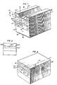
Images
Classifications
-
- H—ELECTRICITY
- H01—ELECTRIC ELEMENTS
- H01L—SEMICONDUCTOR DEVICES NOT COVERED BY CLASS H10
- H01L21/00—Processes or apparatus adapted for the manufacture or treatment of semiconductor or solid state devices or of parts thereof
- H01L21/02—Manufacture or treatment of semiconductor devices or of parts thereof
- H01L21/04—Manufacture or treatment of semiconductor devices or of parts thereof the devices having at least one potential-jump barrier or surface barrier, e.g. PN junction, depletion layer or carrier concentration layer
- H01L21/18—Manufacture or treatment of semiconductor devices or of parts thereof the devices having at least one potential-jump barrier or surface barrier, e.g. PN junction, depletion layer or carrier concentration layer the devices having semiconductor bodies comprising elements of Group IV of the Periodic System or AIIIBV compounds with or without impurities, e.g. doping materials
- H01L21/30—Treatment of semiconductor bodies using processes or apparatus not provided for in groups H01L21/20 - H01L21/26
- H01L21/302—Treatment of semiconductor bodies using processes or apparatus not provided for in groups H01L21/20 - H01L21/26 to change their surface-physical characteristics or shape, e.g. etching, polishing, cutting
- H01L21/306—Chemical or electrical treatment, e.g. electrolytic etching
- H01L21/30604—Chemical etching
- H01L21/30612—Etching of AIIIBV compounds
-
- H—ELECTRICITY
- H01—ELECTRIC ELEMENTS
- H01L—SEMICONDUCTOR DEVICES NOT COVERED BY CLASS H10
- H01L21/00—Processes or apparatus adapted for the manufacture or treatment of semiconductor or solid state devices or of parts thereof
- H01L21/02—Manufacture or treatment of semiconductor devices or of parts thereof
- H01L21/04—Manufacture or treatment of semiconductor devices or of parts thereof the devices having at least one potential-jump barrier or surface barrier, e.g. PN junction, depletion layer or carrier concentration layer
- H01L21/18—Manufacture or treatment of semiconductor devices or of parts thereof the devices having at least one potential-jump barrier or surface barrier, e.g. PN junction, depletion layer or carrier concentration layer the devices having semiconductor bodies comprising elements of Group IV of the Periodic System or AIIIBV compounds with or without impurities, e.g. doping materials
- H01L21/30—Treatment of semiconductor bodies using processes or apparatus not provided for in groups H01L21/20 - H01L21/26
- H01L21/302—Treatment of semiconductor bodies using processes or apparatus not provided for in groups H01L21/20 - H01L21/26 to change their surface-physical characteristics or shape, e.g. etching, polishing, cutting
- H01L21/306—Chemical or electrical treatment, e.g. electrolytic etching
- H01L21/3063—Electrolytic etching
- H01L21/30635—Electrolytic etching of AIIIBV compounds
-
- H—ELECTRICITY
- H01—ELECTRIC ELEMENTS
- H01L—SEMICONDUCTOR DEVICES NOT COVERED BY CLASS H10
- H01L33/00—Semiconductor devices with at least one potential-jump barrier or surface barrier specially adapted for light emission; Processes or apparatus specially adapted for the manufacture or treatment thereof or of parts thereof; Details thereof
- H01L33/005—Processes
- H01L33/0062—Processes for devices with an active region comprising only III-V compounds
-
- H—ELECTRICITY
- H01—ELECTRIC ELEMENTS
- H01S—DEVICES USING THE PROCESS OF LIGHT AMPLIFICATION BY STIMULATED EMISSION OF RADIATION [LASER] TO AMPLIFY OR GENERATE LIGHT; DEVICES USING STIMULATED EMISSION OF ELECTROMAGNETIC RADIATION IN WAVE RANGES OTHER THAN OPTICAL
- H01S5/00—Semiconductor lasers
- H01S5/10—Construction or shape of the optical resonator, e.g. extended or external cavity, coupled cavities, bent-guide, varying width, thickness or composition of the active region
- H01S5/12—Construction or shape of the optical resonator, e.g. extended or external cavity, coupled cavities, bent-guide, varying width, thickness or composition of the active region the resonator having a periodic structure, e.g. in distributed feedback [DFB] lasers
-
- H—ELECTRICITY
- H01—ELECTRIC ELEMENTS
- H01S—DEVICES USING THE PROCESS OF LIGHT AMPLIFICATION BY STIMULATED EMISSION OF RADIATION [LASER] TO AMPLIFY OR GENERATE LIGHT; DEVICES USING STIMULATED EMISSION OF ELECTROMAGNETIC RADIATION IN WAVE RANGES OTHER THAN OPTICAL
- H01S5/00—Semiconductor lasers
- H01S5/10—Construction or shape of the optical resonator, e.g. extended or external cavity, coupled cavities, bent-guide, varying width, thickness or composition of the active region
- H01S5/18—Surface-emitting [SE] lasers, e.g. having both horizontal and vertical cavities
- H01S5/185—Surface-emitting [SE] lasers, e.g. having both horizontal and vertical cavities having only horizontal cavities, e.g. horizontal cavity surface-emitting lasers [HCSEL]
- H01S5/187—Surface-emitting [SE] lasers, e.g. having both horizontal and vertical cavities having only horizontal cavities, e.g. horizontal cavity surface-emitting lasers [HCSEL] using Bragg reflection
-
- H—ELECTRICITY
- H01—ELECTRIC ELEMENTS
- H01S—DEVICES USING THE PROCESS OF LIGHT AMPLIFICATION BY STIMULATED EMISSION OF RADIATION [LASER] TO AMPLIFY OR GENERATE LIGHT; DEVICES USING STIMULATED EMISSION OF ELECTROMAGNETIC RADIATION IN WAVE RANGES OTHER THAN OPTICAL
- H01S5/00—Semiconductor lasers
- H01S5/20—Structure or shape of the semiconductor body to guide the optical wave ; Confining structures perpendicular to the optical axis, e.g. index or gain guiding, stripe geometry, broad area lasers, gain tailoring, transverse or lateral reflectors, special cladding structures, MQW barrier reflection layers
- H01S5/22—Structure or shape of the semiconductor body to guide the optical wave ; Confining structures perpendicular to the optical axis, e.g. index or gain guiding, stripe geometry, broad area lasers, gain tailoring, transverse or lateral reflectors, special cladding structures, MQW barrier reflection layers having a ridge or stripe structure
- H01S5/227—Buried mesa structure ; Striped active layer
-
- H—ELECTRICITY
- H01—ELECTRIC ELEMENTS
- H01S—DEVICES USING THE PROCESS OF LIGHT AMPLIFICATION BY STIMULATED EMISSION OF RADIATION [LASER] TO AMPLIFY OR GENERATE LIGHT; DEVICES USING STIMULATED EMISSION OF ELECTROMAGNETIC RADIATION IN WAVE RANGES OTHER THAN OPTICAL
- H01S5/00—Semiconductor lasers
- H01S5/10—Construction or shape of the optical resonator, e.g. extended or external cavity, coupled cavities, bent-guide, varying width, thickness or composition of the active region
- H01S5/12—Construction or shape of the optical resonator, e.g. extended or external cavity, coupled cavities, bent-guide, varying width, thickness or composition of the active region the resonator having a periodic structure, e.g. in distributed feedback [DFB] lasers
- H01S5/1231—Grating growth or overgrowth details
-
- H—ELECTRICITY
- H01—ELECTRIC ELEMENTS
- H01S—DEVICES USING THE PROCESS OF LIGHT AMPLIFICATION BY STIMULATED EMISSION OF RADIATION [LASER] TO AMPLIFY OR GENERATE LIGHT; DEVICES USING STIMULATED EMISSION OF ELECTROMAGNETIC RADIATION IN WAVE RANGES OTHER THAN OPTICAL
- H01S5/00—Semiconductor lasers
- H01S5/20—Structure or shape of the semiconductor body to guide the optical wave ; Confining structures perpendicular to the optical axis, e.g. index or gain guiding, stripe geometry, broad area lasers, gain tailoring, transverse or lateral reflectors, special cladding structures, MQW barrier reflection layers
- H01S5/22—Structure or shape of the semiconductor body to guide the optical wave ; Confining structures perpendicular to the optical axis, e.g. index or gain guiding, stripe geometry, broad area lasers, gain tailoring, transverse or lateral reflectors, special cladding structures, MQW barrier reflection layers having a ridge or stripe structure
- H01S5/223—Buried stripe structure
-
- H—ELECTRICITY
- H01—ELECTRIC ELEMENTS
- H01S—DEVICES USING THE PROCESS OF LIGHT AMPLIFICATION BY STIMULATED EMISSION OF RADIATION [LASER] TO AMPLIFY OR GENERATE LIGHT; DEVICES USING STIMULATED EMISSION OF ELECTROMAGNETIC RADIATION IN WAVE RANGES OTHER THAN OPTICAL
- H01S5/00—Semiconductor lasers
- H01S5/20—Structure or shape of the semiconductor body to guide the optical wave ; Confining structures perpendicular to the optical axis, e.g. index or gain guiding, stripe geometry, broad area lasers, gain tailoring, transverse or lateral reflectors, special cladding structures, MQW barrier reflection layers
- H01S5/22—Structure or shape of the semiconductor body to guide the optical wave ; Confining structures perpendicular to the optical axis, e.g. index or gain guiding, stripe geometry, broad area lasers, gain tailoring, transverse or lateral reflectors, special cladding structures, MQW barrier reflection layers having a ridge or stripe structure
- H01S5/227—Buried mesa structure ; Striped active layer
- H01S5/2275—Buried mesa structure ; Striped active layer mesa created by etching
Definitions
- This invention relates to a heterostructure junction of the type as defined in the preamble clause of claim 1.
- the DH laser has the longest lifetime of all semiconductor lasers, exceeding 10 s hours to date, and is characterized by low thresholds and fundamental transverse mode operation. On the other hand, it has a wide beam divergence, a nonlinearity (known as a "kink") in its light-current (L-I) characteristic, and incomplete lateral current confinement.
- L-I light-current
- the Tsukada or Burnham BH laser which include a GaAs active layer in form of a narrow strip completely surrounded by Al o . 3 Ga o . 7 As or Al 0,4 Ga 0.6 As, respectively, has effective transverse mode stabilization, but the refractive index change along the junction plane is large with interest to a low lasing threshold current density. This large refractive index change leads to the consequence that only an insignificant amount of the laser radiation leaks outside the active layer and BH lasers of this type operate in higher order radiation modes.
- a fundamental mode lasing is usually preferred which necessarily calls for active layer widths (i.e. stripe widths) of 1 ⁇ m at the most.
- active layers so narrow have a number of disadvantages: They are difficult to fabricate and they result in low-output power (e.g., 1 mW) and large beam divergence in both transverse directions.
- a further heterostructure junction laser type is described by J. C. Campbell et al in IEEE Journal of Quantum Electronics, QE-13 (1977) 253, further by H. Namizaki et al in Applied Physics Letters 31 (1977) 122 and R. A. Logan et al in U.S. patent 39 78 426.
- this laser type comprises four layers. Typically a very thin GaAs active layer and a thicker (GaAI)As guide layer with slight AI content (for instance Ga o. gAl o.
- the problem to be solved by the invention is to provide a new laser combining the advantages of the afore mentioned two laser types without encountering their concomitant disadvantages.
- the active layer stripe of a Tsukada-type laser is optically coupled to a passive waveguide layer in a manner as known per se from the Campbell-type laser in which the active layer does not have such a stripe geometry.
- the inventive SBH (strip buried heterostructure) laser fabricated from the GaAs-AIGaAs materials system exhibited, over a wide operating range a higher power output, surprisingly a linear L-I characteristic for all currents up to catastrophic failure, stable fundamental transverse and single longitudinal mode oscillation and reduced beam divergence, along with adequate lasing thresholds and external quantum efficiencies.
- the active layer stripe is partially embedded in the waveguide layer, which is of low-loss owing to its somewhat greater band gap instead of being formed on top of a major surface of the waveguide layer.
- the portions of the major surface of the waveguide layer adjacent the active layer can be provided with distributed feedback gratings.
- the invention relates also to a method of forming the active region of a heterojunction laser as defined above, in which method a Group III-V compound active epitaxial layer is grown from the liquid phase on an AI-containing Group III-V compound layer. According to the invention this method is characterized by the features of claim 7.
- an SBH laser 10 formed on a substrate 11 and comprising first and . second opposite-conductivity-type, wide bandgap, semiconductor cladding layers 12 and 14 separated by a narrower bandgap, semiconductor region 16 destined for producing and carrying the laser radiation.
- the region 16 includes a low-loss waveguide layer 16.1 and contiguous therewith a narrower bandgap active layer 16.2 in the form of a narrow strip which extends along the longitudinal (resonator) axis 28 of the laser.
- the narrow strip may be formed on top of a major surface of waveguide layer 16.1 as in Fig. 1 or, as shown by layer 16.2' of Fig. 2, may be partially embedded in waveguide layer 16.1'. In the latter case, the major surface of the waveguide layer is essentially coplanar with a major surface of the active layer.
- Means 18 Is provided for constraining pumping current to flow in a narrow channel through the active layer 16.2 (or 16.2') when cladding layers 12 and 14 are forward biased above the lasing threshold. Forward bias voltage is applied by means of suitable ohmic contacts 20 and 22 formed on substrate 11 and means 18, respectively.
- the constraining means 18 comprises a pair of laterally spaced p-n junctions 18.1 and 18.2 which are reverse biased when cladding layers 12 and 14 are forward biased.
- the junctions are formed by depositing on cladding layer 14 a layer 18.3 of the same conductivity type and then forming a bifurcated, wider bandgap layer 18.4 of opposite conductivity type on layer 18.3.
- the junctions 18.1 and 18.2 are thus separated by a window which exposes a strip of layer 18.3. That strip is contacted by the central portion 22.1 of ohmic contact 22 so that pumping current flows transversely through the layers in a narrow channel from contact portion 22.1 in the window to active layer 16.2.
- Current spreading can be further reduced by incorporating an additional pair of spaced, reverse biased p-n junctions at the substrate interface by using prior art schemes.
- the bandgap of cladding layer 14 sufficiently greater than that of active layer 16.2 prevents any substantial amount of pumping current from bypassing the active layer 16.2 by flowing directly between the cladding and waveguide layers; i.e., the turn-on voltage of p-n heterojunctions 16.3 between the waveguide and cladding layers is larger (e.g., 1.6V) than the turn-on voltage of p-n heterojunction 16.4 between the waveguide and active layers (e.g., 1.4 V).
- the pumping current causes the injection of minority carriers into active layer 16.2 where they undergo radiative recombination to generate stimulated radiation.
- a significant portion of the optical field of this radiation penetrates into the waveguide layer 16.1 so as to reduce the optical power density at the mirror facets and thereby increase the threshold for catastrophic damage.
- the bandgap (or refractive index) difference between active layer 16.2 and waveguide layer 16.1 should be small enough to permit such penetration, yet large enough to confine injected minority carriers to the active region and thereby maintain relatively high electronic gain.
- This laser configuration exhibits relatively high pulsed power outputs (in the hundreds of milliwatts range) and, surprisingly, a linear L characteristic being free of kinks at all power levels up to the catastrophic damage threshold.
- this SBH laser exhibited stable fundamental transverse and single longitudinal mode operation.
- these materials include, for example, GaAs-AIGaAs, GaAs-AIGaAsP, GaAsSb-AIGaAsSb and InP-lnGaAsP.
- GaAs-AIGaAs has the advantage that it is substantially lattice matched over all solid solutions of GaAs and AlAs. Using the latter system, the SBH laser of Fig.
- n-GaAs substrate on which the following layers would be epitaxially grown: an n-Al x Ga,_ x As cladding layer 12 (0 ⁇ x ⁇ 1); an n-Al y Ga 1-y As waveguide layer 16.1 (0 ⁇ y ⁇ 1;y ⁇ x); an n-, p- or compensated active layer 16.2 of Al z Ga 1-z As [0 ⁇ z ⁇ 0.4; z ⁇ y; and (y-z) adapted to confine injected carriers to the active layer while at the same time permitting the optical field to penetrate from the active iayer into the waveguide layer]; a p-AlqGa 1-q As cladding layer 14 [0 ⁇ q ⁇ 1; q>z and y; and (q-y)>(y-z) to prevent significant pumping current from flowing across heterojunctions 16.3]; a p-GaAs stop-etch and contacting layer 18.3, and an n-Al r Ga 1-r As bifurcated layer 18.4
- the SBH laser is mounted on a heat sink (not shown), and for continuous wave operation at room temperature, the thickness of the active layer 16.2 should be less than 1.0 ⁇ m and preferably about 0.15-0.20 ⁇ m.
- the SBH laser incorporates a distributed feedback (DFB) grating which provides frequency selectivity and in integrated optics applications obviates the need for a discrete resonator formed by cleaved mirror facets.
- the DFB grating comprises a plurality of parallel grooves 30 which are formed on the same major surface of waveguide layer 16.1 as active layer 16.2, i.e., on heterojunctions 16.3. But, the grooves are formed on opposite sides of the active layer 16.2 and extend perpendicular to the resonator axis 28 (i.e., perpendicular to the elongated dimension of strip active layer 16.2).
- the periodicity of the grating should preferably be equal to an odd integral number of half wavelengths of the laser radiation as measured in the semiconductor.
- This grating would typically be formed, for example, by ion milling or chemically etching waveguide layer 16.1 after depositing and suitably masking active layer 16.2.
- the interior ends of the grating grooves should preferably be as close to the sides of the active layer as possible to allow the optical field in the active layer 16.2 to penetrate into the grating.
- the grating ends should be within 1-2 um of the active region.
- the interior ends of the grating grooves can be made right next to the sides of the embedded active strip 16.2' by fabricating the grating first, uniformly everywhere, then etching the channel for the embedded strip 16.2'.
- BH buried heterostructure
- effective transverse mode stabilization has been achieved by introducing a built-in refractive index change along the junction plane; for example, by embedding an active GaAs core completely in Al 0.3 Ga 0.7 As cladding, see Tsukada et al supra.
- the index change along the junction plane is so large that stable fundamental mode lasing is possible only for active layer widths of ⁇ 1 ⁇ m, resulting in low output power and large beam divergence in the two transverse directions.
- higher order modes are easily excited near threshold.
- the introduction of the waveguide layer converts the core in a BH laser to a strip-loaded waveguide having the thin active layer in form of a strip and the thicker low-loss waveguide as the supporting layer.
- This structure significantly reduces the effective refractive index change along the junction plane.
- fundamental transverse mode along the junction plane can be easily obtained with much wider strip widths.
- the output power is increased and the beam divergence is reduced, while mode stabilization is maintained.
- better device fabrication and performance control can be achieved.
- the introduction of the waveguide layer greatly increases the cavity thickness (e.g., from about 0.2 ⁇ m to about 1.6 ⁇ m) while still providing enough potential barrier to confine the injected carriers in the active strip.
- This thickening of the optical cavity does not affect the threshold current but increases the output power before catastrophic mirror failure and reduces the beam divergence.
- the active strip is much thinner than the waveguide layer, the fundamental transverse mode (perpendicular to the junction plane) acquires more gain than higher order modes. This provides mode discrimination against higher order modes even though they have slightly higher mirror reflectivity.
- the waveguide layer is not expected to decrease the quantum efficiency of the laser because it is essentially lossless at the lasing wavelength.
- SBH lasers of the type depicted in Fig. 1 have been fabricated to comprise: an (001) n-GaAs substrate 11 doped with Si to about 10' 8 cm- 3 and about 100 ⁇ m thick; an n-Al 0.3 Ga 0.7 As cladding layer 12 doped with Sn to about 2x10" cm- 3 and about 1.4 ⁇ m thick; an n-Al 0.1 Ga 0.9 As waveguide layer 16.1 doped with Sn to about 2 ⁇ 10 17 cm- 3 ; a p-GaAs active layer 16.2 doped with Ge to about 3 ⁇ 10 17 cm- 3 and about 0.2 ⁇ m thick and of various widths-2.5, 3.5, 5, 7.5 or 10 ⁇ m; a p-Al 0.3 Ga 0.7 As cladding layer 14 doped with Ge to about 3x10" cm- 3 and about 2.5
- LPE liquid phase epitaxy
- SBH lasers proceeded as follows. During the first LPE growth cycle, layers 12 and 16.1 as described above were deposited on an n-GaAs wafer (i.e., on the substrate 11) and then a p-GaAs layer was deposited having a thickness equal to that desired for the active layer 16.2 and serving also as a protective layer for the layer 16.1. A thin (about 0.2 ⁇ m) p-Al 0.3 Ga 0.7 As layer was then grown on the p-GaAs layer. Note, the last layer was deposited to protect the top interface of the p-GaAs layer during subsequent processing steps, it acts as a prior-protective layer and does not yet correspond to the much thicker cladding layer 14.
- This intermediate structure was removed from the LPE chamber, and the top surface of the thin Al 0.3 Ga 0.7 As layer was anodized to form a native oxide masking layer thereon.
- Standard photolithographic techniques were then used to form mask strips along the (110) direction in the oxide layer and to expose the thin Al 0.3 Ga 0.7 As prior protective layer between the strips.
- the exposed AI 0.3 Ga 0.7 As was selectively etched in an iodine etchant (113 g KI, 65 g 1 2 , 100 cc H 2 0) to expose the p-GaAs layer between the strips.
- Standard anodization (which forms a native oxide and consumes a portion of the semiconductor) and stripping were then used to remove nearly all of the p-GaAs layer between the strips.
- the structure on the wafer comprised layers 12 and 16.1 with strip mesas of p-GaAs (i.e., active layer 16.2) protected by the thin Al 0.3 Ga 0.7 As prior-protective layer.
- the spaces between mesas were protected with the thin (about 20 nm thick) p-GaAs layer.
- the wafer was returned to the LPE chamber and p-Al 0.3 Ga 0.7 As layer 14 was grown thereon.
- the thin pAl 0.3 Ga 0.7 As prior-protective layers protecting the tops of the p-GaAs layers were incorporated into layer 14, and the thin p-GaAs layer between the strips was dissolved into the melt used to grow layer 14. Therefore, layer 14; for all practical purposes, grew directly on the portions of waveguide layer 16.1 between the strips as well as on the strips themselves.
- the contacting and stop-etch p-GaAs layer 18.3 was then grown followed by an n-Al 0.45 Ga 0.55 As layer.
- the latter was masked, using the same photolithographic mask used to define the strips, and then selectively etched, using the iodine etchant previously described, down to the p-GaAs layer 18.3, thereby bifurcating the n-Al 0.45 Ga 0.55 As layer as depicted by layer 18.4 of Fig. 1.
- Individual SBH laser diodes were then formed by conventional metallization, cleaving and heat-sinking procedures.
- Light-current (L-I) characteristics of the SBH lasers without anti-reflection mirror coatings were made using standard measurement procedures. The measurements with pulsed injection (150 ns pulse width, 1000 pulses/sec) were made for active layer widths of about 5 ⁇ m and 10 gm and lengths of 380 ⁇ m. The top channel (window in layer 18.4) widths of the lasers with 10 gm and 5 um wide active strips were typically about 15 ⁇ m and 10 ⁇ m. respectively. All lasers tested displayed excellent linearity in L-I characteristics. For lasers with 10 ⁇ m strips, this linearity continued, without catastrophic failure, to about 10 times threshold current where a peak power output of 400 mW per face was measured.
- the far-field patterns, both along and perpendicular to the junction plsne, at various current levels above threshold were also measured for a typical SBH laser with a nominal 5 um wide active layer. These patterns were measured under pulsed operation up to 9 times threshold. In the current region examined, the lasers operated stably in the fundamental mode in both transverse directions with no significant distortion of the field patterns. In general, the beam divergences were about 8-10 degrees and 26-30 degrees in the directions parallel and perpendicular to the junction plane, respectively. For lasers with 10 ⁇ m wide active layers, higher order modes along the junction plane were excited near threshold and successively changed into even higher order modes as the current injection level was increased. However, no "kink" or other nonlinearity associated with mode transition have been observed.
- lasing occurred in several longitudinal modes at slightly above the threshold current I th ( ⁇ 1.05 I th ) ' but the lasing power quickly concentrated into a single longitudinal mode with a slight increase in current.
- the longitudinal mode With increasing current, the longitudinal mode shifted to an adjacent shorter wavelength mode, staying predominantly a single mode over wide current intervals except during the brief mode transitions. Such current intervals shortened for high injection current levels.
- the strip active layer in each of the embodiments of the SBH laser it is readily possible to fabricate the strip active layer so that it is shorter than the resonator (i.e., the active layer terminates short of the mirror facets), thereby virtually eliminating surface recombination of the facets.
- the active layer would be entirely embedded in wider bandgap material.
- the DFB gratings near the facets can be made to extend across the width of the laser.
Description
- This invention relates to a heterostructure junction of the type as defined in the preamble clause of claim 1.
- A stripe-geometry contact for junction lasers was proposed by R. A. Furnanage et al (U.S. patent No. 3,363,195, granted January 9, 1968) more than a decade ago and has been incorporated, in one form or another, in various heterostructure laser configurations in use and understudy today. These lasers, which range from the simple double heterostructure (DH) (I. Hayashi, U.S. patent 3,758,875, granted September 11, 1973) to more complicated buried heterostructures (BH) (T. Tsukada, Journal of Applied Physics, 45, (1974) 4899 or R. D. Burnham et al, Applied Physics Letters 27 (1975) 510), each have one or more advantageous operating characteristics.
- The DH laser has the longest lifetime of all semiconductor lasers, exceeding 10s hours to date, and is characterized by low thresholds and fundamental transverse mode operation. On the other hand, it has a wide beam divergence, a nonlinearity (known as a "kink") in its light-current (L-I) characteristic, and incomplete lateral current confinement.
- The Tsukada or Burnham BH laser, which include a GaAs active layer in form of a narrow strip completely surrounded by Alo.3Gao.7As or Al0,4Ga0.6As, respectively, has effective transverse mode stabilization, but the refractive index change along the junction plane is large with interest to a low lasing threshold current density. This large refractive index change leads to the consequence that only an insignificant amount of the laser radiation leaks outside the active layer and BH lasers of this type operate in higher order radiation modes. However, a fundamental mode lasing is usually preferred which necessarily calls for active layer widths (i.e. stripe widths) of 1 µm at the most. But, active layers so narrow have a number of disadvantages: They are difficult to fabricate and they result in low-output power (e.g., 1 mW) and large beam divergence in both transverse directions.
- A further heterostructure junction laser type is described by J. C. Campbell et al in IEEE Journal of Quantum Electronics, QE-13 (1977) 253, further by H. Namizaki et al in Applied Physics Letters 31 (1977) 122 and R. A. Logan et al in U.S. patent 39 78 426. Basically this laser type comprises four layers. Typically a very thin GaAs active layer and a thicker (GaAI)As guide layer with slight AI content (for instance Gao.gAlo.,As according to Namizaki, or Ga0.85Al0.15As according to Campbell) are sandwiched between (GaAI)As confining layers with higher AI content (for instance Ga0.7Al0.3As according to Namizaki, or from Ga0.7Al0.3As to Ga0.6Al0.4As according to Campbell) of opposite conductivity type. Although recombination radiation takes place in the active layer as a result of a minority carrier confinement to the active layer owing to the existing band gap difference between the guide layer and the active layer, the optical field of the guided mode spreads over both the active layer and the guide layer, since there is only a small refractive index difference between these two layers.
- In effect there is a stronger optical coupling by evanescent fields between the active layer and the adjacent passive optical wave guide layer. While this laser configuration has an improved output power and some other advantages over the Tsukada laser, it still suffers from several disadvantages. One is the presence of nonlinearities or kinks in the light-current (LI) characteristic; other are still relatively low power and instability of transverse and longitudinal mode oscillations.
- Accordingly the problem to be solved by the invention is to provide a new laser combining the advantages of the afore mentioned two laser types without encountering their concomitant disadvantages.
- According to the invention this problem is solved for a laser of the type as defined in the preamble clause of claim 1 with the features of the characterizing clause of claim 1.
- In other words, according to the invention the active layer stripe of a Tsukada-type laser is optically coupled to a passive waveguide layer in a manner as known per se from the Campbell-type laser in which the active layer does not have such a stripe geometry.
- For example, the inventive SBH (strip buried heterostructure) laser fabricated from the GaAs-AIGaAs materials system exhibited, over a wide operating range a higher power output, surprisingly a linear L-I characteristic for all currents up to catastrophic failure, stable fundamental transverse and single longitudinal mode oscillation and reduced beam divergence, along with adequate lasing thresholds and external quantum efficiencies.
- In other embodiments of the invention, the active layer stripe is partially embedded in the waveguide layer, which is of low-loss owing to its somewhat greater band gap instead of being formed on top of a major surface of the waveguide layer. In either case, however, the portions of the major surface of the waveguide layer adjacent the active layer can be provided with distributed feedback gratings.
- Further developments of the invention are the subject matter of the subclaims 2 to 6.
- Additionally, the invention relates also to a method of forming the active region of a heterojunction laser as defined above, in which method a Group III-V compound active epitaxial layer is grown from the liquid phase on an AI-containing Group III-V compound layer. According to the invention this method is characterized by the features of claim 7.
- The invention is now described in greater detail in conjunction with the drawing, in which the fig. are not drawn to scale for clarity of illustration. In the drawing:
- Fig. 1 is a schematic isometric view of an SBH laser in accordance with one embodiment of our invention in which the strip active layer is formed on top of a major surface of the waveguide layer;
- Fig. 2 is an end view of an SBH laser in accordance with another embodiment of our invention in which the strip active layer is partially embedded in the waveguide layer; and
- Fig. 3 is a schematic isometric view of an SBH laser in accordance with yet another embodiment of our invention in which distributed feedback gratings flank the strip active layer.
- With reference now to Fig. 1, there is shown an
SBH laser 10 formed on a substrate 11 and comprising first and . second opposite-conductivity-type, wide bandgap,semiconductor cladding layers 12 and 14 separated by a narrower bandgap,semiconductor region 16 destined for producing and carrying the laser radiation. Theregion 16 includes a low-loss waveguide layer 16.1 and contiguous therewith a narrower bandgap active layer 16.2 in the form of a narrow strip which extends along the longitudinal (resonator)axis 28 of the laser. The narrow strip may be formed on top of a major surface of waveguide layer 16.1 as in Fig. 1 or, as shown by layer 16.2' of Fig. 2, may be partially embedded in waveguide layer 16.1'. In the latter case, the major surface of the waveguide layer is essentially coplanar with a major surface of the active layer. -
Means 18 Is provided for constraining pumping current to flow in a narrow channel through the active layer 16.2 (or 16.2') when claddinglayers 12 and 14 are forward biased above the lasing threshold. Forward bias voltage is applied by means ofsuitable ohmic contacts - In the embodiment shown, the constraining means 18 comprises a pair of laterally spaced p-n junctions 18.1 and 18.2 which are reverse biased when cladding
layers 12 and 14 are forward biased. The junctions are formed by depositing on cladding layer 14 a layer 18.3 of the same conductivity type and then forming a bifurcated, wider bandgap layer 18.4 of opposite conductivity type on layer 18.3. The junctions 18.1 and 18.2 are thus separated by a window which exposes a strip of layer 18.3. That strip is contacted by the central portion 22.1 ofohmic contact 22 so that pumping current flows transversely through the layers in a narrow channel from contact portion 22.1 in the window to active layer 16.2. Current spreading can be further reduced by incorporating an additional pair of spaced, reverse biased p-n junctions at the substrate interface by using prior art schemes. - In addition, making the bandgap of
cladding layer 14 sufficiently greater than that of active layer 16.2 prevents any substantial amount of pumping current from bypassing the active layer 16.2 by flowing directly between the cladding and waveguide layers; i.e., the turn-on voltage of p-n heterojunctions 16.3 between the waveguide and cladding layers is larger (e.g., 1.6V) than the turn-on voltage of p-n heterojunction 16.4 between the waveguide and active layers (e.g., 1.4 V). - The pumping current causes the injection of minority carriers into active layer 16.2 where they undergo radiative recombination to generate stimulated radiation. A significant portion of the optical field of this radiation penetrates into the waveguide layer 16.1 so as to reduce the optical power density at the mirror facets and thereby increase the threshold for catastrophic damage. To this end the bandgap (or refractive index) difference between active layer 16.2 and waveguide layer 16.1 should be small enough to permit such penetration, yet large enough to confine injected minority carriers to the active region and thereby maintain relatively high electronic gain. This laser configuration, as has been found, exhibits relatively high pulsed power outputs (in the hundreds of milliwatts range) and, surprisingly, a linear L characteristic being free of kinks at all power levels up to the catastrophic damage threshold. In addition, this SBH laser exhibited stable fundamental transverse and single longitudinal mode operation.
- In order to reduce the number of non- radiative recombination defect centers at the heterojunction interfaces between the various layers of our SBH laser, it is preferred that essentially lattice matched materials be utilized. Fewer defect centers generally lead to lower lasing thresholds and longer lifetimes. In the Group III-V compound system these materials include, for example, GaAs-AIGaAs, GaAs-AIGaAsP, GaAsSb-AIGaAsSb and InP-lnGaAsP. Of these, GaAs-AIGaAs has the advantage that it is substantially lattice matched over all solid solutions of GaAs and AlAs. Using the latter system, the SBH laser of Fig. 1 would typically comprise an n-GaAs substrate on which the following layers would be epitaxially grown: an n-AlxGa,_xAs cladding layer 12 (0<x<1); an n-AlyGa1-yAs waveguide layer 16.1 (0<y<1;y<x); an n-, p- or compensated active layer 16.2 of AlzGa1-zAs [0≤z<0.4; z<y; and (y-z) adapted to confine injected carriers to the active layer while at the same time permitting the optical field to penetrate from the active iayer into the waveguide layer]; a p-AlqGa1-qAs cladding layer 14 [0<q<1; q>z and y; and (q-y)>(y-z) to prevent significant pumping current from flowing across heterojunctions 16.3]; a p-GaAs stop-etch and contacting layer 18.3, and an n-AlrGa1-rAs bifurcated layer 18.4 (0<r<1). Of course, the conductivity types of the various layers can be reversed.
- For efficient operation at room temperature the SBH laser is mounted on a heat sink (not shown), and for continuous wave operation at room temperature, the thickness of the active layer 16.2 should be less than 1.0 µm and preferably about 0.15-0.20 µm.
- An alternative embodiment of the SBH laser incorporates a distributed feedback (DFB) grating which provides frequency selectivity and in integrated optics applications obviates the need for a discrete resonator formed by cleaved mirror facets. As shown in Fig. 3, the DFB grating comprises a plurality of
parallel grooves 30 which are formed on the same major surface of waveguide layer 16.1 as active layer 16.2, i.e., on heterojunctions 16.3. But, the grooves are formed on opposite sides of the active layer 16.2 and extend perpendicular to the resonator axis 28 (i.e., perpendicular to the elongated dimension of strip active layer 16.2). As is well known in the art, to provide feedback the periodicity of the grating should preferably be equal to an odd integral number of half wavelengths of the laser radiation as measured in the semiconductor. This grating would typically be formed, for example, by ion milling or chemically etching waveguide layer 16.1 after depositing and suitably masking active layer 16.2. Note that the interior ends of the grating grooves should preferably be as close to the sides of the active layer as possible to allow the optical field in the active layer 16.2 to penetrate into the grating. Illustratively, the grating ends should be within 1-2 um of the active region. Although not depicted, the DFB configuration of Fig. 3 could also be incorporated into the embodiment of Fig. 2 by forming the grating, as before, on the heterojunctions 16.3' on opposite sides of active layer 16.2'. In this case, the interior ends of the grating grooves can be made right next to the sides of the embedded active strip 16.2' by fabricating the grating first, uniformly everywhere, then etching the channel for the embedded strip 16.2'. - In prior art buried heterostructure (BH) lasers, effective transverse mode stabilization has been achieved by introducing a built-in refractive index change along the junction plane; for example, by embedding an active GaAs core completely in Al0.3Ga0.7As cladding, see Tsukada et al supra. However, the index change along the junction plane is so large that stable fundamental mode lasing is possible only for active layer widths of ≤1 µm, resulting in low output power and large beam divergence in the two transverse directions. Yet, in lasers with wider active layers, higher order modes are easily excited near threshold.
- In the present SBH laser, the introduction of the waveguide layer converts the core in a BH laser to a strip-loaded waveguide having the thin active layer in form of a strip and the thicker low-loss waveguide as the supporting layer. This structure significantly reduces the effective refractive index change along the junction plane. Hence, fundamental transverse mode along the junction plane can be easily obtained with much wider strip widths. As a result, the output power is increased and the beam divergence is reduced, while mode stabilization is maintained. Furthermore, better device fabrication and performance control can be achieved.
- In the direction perpenaicular to the junction plane, the introduction of the waveguide layer greatly increases the cavity thickness (e.g., from about 0.2 µm to about 1.6 µm) while still providing enough potential barrier to confine the injected carriers in the active strip. This thickening of the optical cavity does not affect the threshold current but increases the output power before catastrophic mirror failure and reduces the beam divergence. Since the active strip is much thinner than the waveguide layer, the fundamental transverse mode (perpendicular to the junction plane) acquires more gain than higher order modes. This provides mode discrimination against higher order modes even though they have slightly higher mirror reflectivity. Finally, the waveguide layer is not expected to decrease the quantum efficiency of the laser because it is essentially lossless at the lasing wavelength. Therefore, low current threshold, stable fundamental transverse mode operation with surprisingly linear light-current characteristic and narrow beam divergence in both transverse directions up to substantially high injection current levels, and high output power should be obtainable with the present SBH lasers. Indeed these properties have been observed as discussed in the example which follows..
- The following describes the fabrication of an SBH laser from the GaAs-AIGaAs system. Dimensions, materials, conductivity types and carrier concentrations are intended to be illustrative only and should not be construed as limitations on the scope of the invention.
- Using a two-cycle liquid phase epitaxy (LPE) technique, with suitable masking, etching and anodization steps between the two cycles, SBH lasers of the type depicted in Fig. 1 have been fabricated to comprise: an (001) n-GaAs substrate 11 doped with Si to about 10'8 cm-3 and about 100 µm thick; an n-Al0.3Ga0.7As cladding layer 12 doped with Sn to about 2x10" cm-3 and about 1.4 µm thick; an n-Al0.1Ga0.9As waveguide layer 16.1 doped with Sn to about 2 × 1017 cm-3; a p-GaAs active layer 16.2 doped with Ge to about 3 × 1017 cm-3 and about 0.2 µm thick and of various widths-2.5, 3.5, 5, 7.5 or 10 µm; a p-Al0.3Ga0.7As
cladding layer 14 doped with Ge to about 3x10" cm-3 and about 2.5 um thick; a p-GaAs contacting and stop-etch layer 18.3 doped with Ge to about 5x10" cm-3 and about 0.5 um thick; and an n-Al0.45Ga0.55As layer 18.4 doped with Sn to about 1017cm-3 and about 1 um thick. The layer 18.4 had various window openings of comparable size to the underlying active strips 16.2 and in substantial registration therewith. Thesubstrate contact 20 comprised a Au-Sn alloy whereas thetop contact 22 comprised a Au-Zn alloy. - The fabrication of these SBH lasers proceeded as follows. During the first LPE growth cycle, layers 12 and 16.1 as described above were deposited on an n-GaAs wafer (i.e., on the substrate 11) and then a p-GaAs layer was deposited having a thickness equal to that desired for the active layer 16.2 and serving also as a protective layer for the layer 16.1. A thin (about 0.2 µm) p-Al0.3Ga0.7As layer was then grown on the p-GaAs layer. Note, the last layer was deposited to protect the top interface of the p-GaAs layer during subsequent processing steps, it acts as a prior-protective layer and does not yet correspond to the much
thicker cladding layer 14. This intermediate structure was removed from the LPE chamber, and the top surface of the thin Al0.3Ga0.7As layer was anodized to form a native oxide masking layer thereon. Standard photolithographic techniques were then used to form mask strips along the (110) direction in the oxide layer and to expose the thin Al0.3Ga0.7As prior protective layer between the strips. The exposed AI0.3Ga0.7As was selectively etched in an iodine etchant (113 g KI, 65 g 12, 100 cc H20) to expose the p-GaAs layer between the strips. Standard anodization (which forms a native oxide and consumes a portion of the semiconductor) and stripping were then used to remove nearly all of the p-GaAs layer between the strips. It was important, however, to leave a thin (about 20 nm thick) remainder of the p-GaAs layer between the strips so as not to expose the underlying n-Al0.1Ga0.9As to the atmosphere. Such exposure makes subsequent LPE growth on AI-containing Group III-V compounds very difficult - After removing the oxide strip masks ana subsequent chemical cleaning, the structure on the wafer comprised layers 12 and 16.1 with strip mesas of p-GaAs (i.e., active layer 16.2) protected by the thin Al0.3Ga0.7As prior-protective layer. The spaces between mesas were protected with the thin (about 20 nm thick) p-GaAs layer.
- Next, the wafer was returned to the LPE chamber and p-Al0.3Ga0.7As
layer 14 was grown thereon. During this growth step the thin pAl0.3Ga0.7As prior-protective layers protecting the tops of the p-GaAs layers were incorporated intolayer 14, and the thin p-GaAs layer between the strips was dissolved into the melt used to growlayer 14. Therefore,layer 14; for all practical purposes, grew directly on the portions of waveguide layer 16.1 between the strips as well as on the strips themselves. - The contacting and stop-etch p-GaAs layer 18.3 was then grown followed by an n-Al0.45Ga0.55As layer. The latter was masked, using the same photolithographic mask used to define the strips, and then selectively etched, using the iodine etchant previously described, down to the p-GaAs layer 18.3, thereby bifurcating the n-Al0.45Ga0.55As layer as depicted by layer 18.4 of Fig. 1. Individual SBH laser diodes were then formed by conventional metallization, cleaving and heat-sinking procedures.
- Light-current (L-I) characteristics of the SBH lasers without anti-reflection mirror coatings were made using standard measurement procedures. The measurements with pulsed injection (150 ns pulse width, 1000 pulses/sec) were made for active layer widths of about 5 µm and 10 gm and lengths of 380 µm. The top channel (window in layer 18.4) widths of the lasers with 10 gm and 5 um wide active strips were typically about 15 µm and 10 µm. respectively. All lasers tested displayed excellent linearity in L-I characteristics. For lasers with 10 µm strips, this linearity continued, without catastrophic failure, to about 10 times threshold current where a peak power output of 400 mW per face was measured. One laser with a 5 µm strip was tested to the catastrophic failure limit. For that laser linearity continued up to about 15 times threshold at which a peak power output of 230 mW per face was measured. At this power catastrophic failure occurred. Similarly, measurements of the light-current characteristics of other SBH lasers with 5 µm wide active layers have been performed; those lasers have been pumped only to an output power of 100 mW per face to avoid burnout. The uniformity and linearity of the lasers was evident.
- For SBH lasers with 10 µm and 5 µm wide active layers, current thresholds were 150 mA-180 mA and 90 mA-150 mA, respectively, while the external quantum efficiencies were 44%―63% and 25%―35%. The lower external quantum efficiency of the lasers with 5 µm strips was due to: (1) the larger top channel- to-strip width ratio, about 2, as compared to about 1.5 for lasers with 10 µm strips, and (2) the fact that as the top channel width decreases, the amount of lateral current spreading in the p-GaAs and p-Al0.3Ga0.7As layers increases rapidly. By using more efficient lateral current confinement schemes, such as laterally spaced, reverse-biased junctions at the substrate interface in addition to those of Fig. 1, it is believed that much lower current thresholds can be obtained.
- The far-field patterns, both along and perpendicular to the junction plsne, at various current levels above threshold were also measured for a typical SBH laser with a nominal 5 um wide active layer. These patterns were measured under pulsed operation up to 9 times threshold. In the current region examined, the lasers operated stably in the fundamental mode in both transverse directions with no significant distortion of the field patterns. In general, the beam divergences were about 8-10 degrees and 26-30 degrees in the directions parallel and perpendicular to the junction plane, respectively. For lasers with 10 µm wide active layers, higher order modes along the junction plane were excited near threshold and successively changed into even higher order modes as the current injection level was increased. However, no "kink" or other nonlinearity associated with mode transition have been observed. Lasers with 5 µm wide active layers, under pulsed operation, exhibited single longitudinal mode oscillation at injection currents as high as twice threshold. In general, lasing occurred in several longitudinal modes at slightly above the threshold current Ith (<1.05 Ith)' but the lasing power quickly concentrated into a single longitudinal mode with a slight increase in current. With increasing current, the longitudinal mode shifted to an adjacent shorter wavelength mode, staying predominantly a single mode over wide current intervals except during the brief mode transitions. Such current intervals shortened for high injection current levels.
- Numerous and varied other arrangements can be devised. For example, in each of the embodiments of the SBH laser it is readily possible to fabricate the strip active layer so that it is shorter than the resonator (i.e., the active layer terminates short of the mirror facets), thereby virtually eliminating surface recombination of the facets. Thus, the active layer would be entirely embedded in wider bandgap material. Also note that with this modification to Fig. 3, the DFB gratings near the facets can be made to extend across the width of the laser.
Claims (7)
Applications Claiming Priority (2)
| Application Number | Priority Date | Filing Date | Title |
|---|---|---|---|
| US865237 | 1977-12-28 | ||
| US05/865,237 US4190813A (en) | 1977-12-28 | 1977-12-28 | Strip buried heterostructure laser |
Related Child Applications (3)
| Application Number | Title | Priority Date | Filing Date |
|---|---|---|---|
| EP81100580.0 Division-Into | 1978-12-28 | ||
| EP81100580A Division EP0031808A3 (en) | 1977-12-28 | 1978-12-28 | Method of growing a group iii-v compound epitaxial second layer from the liquid phase on an al-containing group iii-v compound layer |
| EP81100580A Division-Into EP0031808A3 (en) | 1977-12-28 | 1978-12-28 | Method of growing a group iii-v compound epitaxial second layer from the liquid phase on an al-containing group iii-v compound layer |
Publications (3)
| Publication Number | Publication Date |
|---|---|
| EP0002827A2 EP0002827A2 (en) | 1979-07-11 |
| EP0002827A3 EP0002827A3 (en) | 1979-07-25 |
| EP0002827B1 true EP0002827B1 (en) | 1982-06-30 |
Family
ID=25345023
Family Applications (2)
| Application Number | Title | Priority Date | Filing Date |
|---|---|---|---|
| EP81100580A Withdrawn EP0031808A3 (en) | 1977-12-28 | 1978-12-28 | Method of growing a group iii-v compound epitaxial second layer from the liquid phase on an al-containing group iii-v compound layer |
| EP78101846A Expired EP0002827B1 (en) | 1977-12-28 | 1978-12-28 | Strip buried heterostructure laser and method for producing same |
Family Applications Before (1)
| Application Number | Title | Priority Date | Filing Date |
|---|---|---|---|
| EP81100580A Withdrawn EP0031808A3 (en) | 1977-12-28 | 1978-12-28 | Method of growing a group iii-v compound epitaxial second layer from the liquid phase on an al-containing group iii-v compound layer |
Country Status (6)
| Country | Link |
|---|---|
| US (1) | US4190813A (en) |
| EP (2) | EP0031808A3 (en) |
| JP (1) | JPS6058598B2 (en) |
| CA (1) | CA1134485A (en) |
| IT (1) | IT1108267B (en) |
| WO (1) | WO1979000445A1 (en) |
Families Citing this family (28)
| Publication number | Priority date | Publication date | Assignee | Title |
|---|---|---|---|---|
| US4302729A (en) * | 1979-05-15 | 1981-11-24 | Xerox Corporation | Channeled substrate laser with distributed feedback |
| US4276098A (en) * | 1980-03-31 | 1981-06-30 | Bell Telephone Laboratories, Incorporated | Batch processing of semiconductor devices |
| US4445218A (en) * | 1981-09-28 | 1984-04-24 | Bell Telephone Laboratories, Incorporated | Semiconductor laser with conductive current mask |
| JPS5858788A (en) * | 1981-10-05 | 1983-04-07 | Fujitsu Ltd | Semiconductor light-emitting device and its manufacture |
| JPS5898996A (en) * | 1981-12-03 | 1983-06-13 | ゼロツクス・コ−ポレ−シヨン | Injection type laser |
| US4461007A (en) * | 1982-01-08 | 1984-07-17 | Xerox Corporation | Injection lasers with short active regions |
| EP0106305B1 (en) * | 1982-10-12 | 1989-03-15 | Nec Corporation | Double heterostructure semiconductor laser with periodic structure formed in guide layer |
| JPS59129486A (en) * | 1983-01-14 | 1984-07-25 | Toshiba Corp | Semiconductor laser device and manufacture thereof |
| DE3483733D1 (en) * | 1983-04-27 | 1991-01-24 | Toshiba Kawasaki Kk | SEMICONDUCTOR LASER. |
| JPS59205787A (en) * | 1983-05-09 | 1984-11-21 | Nec Corp | Single axial mode semiconductor laser |
| JPH0632339B2 (en) * | 1984-12-18 | 1994-04-27 | キヤノン株式会社 | Semiconductor laser |
| US4600469A (en) * | 1984-12-21 | 1986-07-15 | Honeywell Inc. | Method for polishing detector material |
| US4722092A (en) * | 1985-01-30 | 1988-01-26 | Massachusetts Institute Of Technology | GaInAsP/InP distributed feedback laser |
| US4777148A (en) * | 1985-01-30 | 1988-10-11 | Massachusetts Institute Of Technology | Process for making a mesa GaInAsP/InP distributed feedback laser |
| JPH0722214B2 (en) * | 1985-07-18 | 1995-03-08 | シャープ株式会社 | Method for manufacturing semiconductor laser device |
| FR2587852B1 (en) * | 1985-09-24 | 1989-04-07 | Chaminant Guy | METHOD FOR PRODUCING A LASER WITH A SEMICONDUCTOR WITH A TUBE BURIED WITH OR WITHOUT A DIFFRACTION NETWORK AND LASER OBTAINED BY THIS PROCESS |
| JPS6273690A (en) * | 1985-09-26 | 1987-04-04 | Sharp Corp | Semiconductor laser element |
| FR2596529B1 (en) * | 1986-03-28 | 1988-05-13 | Thomson Csf | OPTICAL WAVEGUIDE IN SEMICONDUCTOR MATERIAL, LASER APPLYING THE SAME AND WAVEGUIDE |
| JPS63140591A (en) * | 1986-12-02 | 1988-06-13 | Mitsubishi Electric Corp | Manufacture of semiconductor laser device |
| JPS6415913A (en) * | 1987-07-09 | 1989-01-19 | Mitsubishi Monsanto Chem | Epitaxial growth method of substrate for high-brightness led |
| JPH0770755B2 (en) * | 1988-01-21 | 1995-07-31 | 三菱化学株式会社 | High brightness LED epitaxial substrate and method of manufacturing the same |
| US5119388A (en) * | 1989-02-24 | 1992-06-02 | Laser Photonics, Inc. | Low tuning rate PbTe/PbEuSeTe buried quantum well tunable diode lasers and arrays |
| US5028563A (en) * | 1989-02-24 | 1991-07-02 | Laser Photonics, Inc. | Method for making low tuning rate single mode PbTe/PbEuSeTe buried heterostructure tunable diode lasers and arrays |
| NL8902292A (en) * | 1989-09-14 | 1991-04-02 | Philips Nv | METHOD FOR MANUFACTURING A MESA CONTAINING SEMICONDUCTOR DEVICE |
| JP2547464B2 (en) * | 1990-04-13 | 1996-10-23 | シャープ株式会社 | Method for manufacturing semiconductor laser device |
| AU4557300A (en) | 1999-04-27 | 2000-11-10 | Karandashov, Sergey | Radiation source |
| JP2007510302A (en) * | 2003-10-31 | 2007-04-19 | ブッカム テクノロジー ピーエルシー | Method for producing a diffraction grating in an easily oxidized semiconductor material |
| JP2008177430A (en) * | 2007-01-19 | 2008-07-31 | Sony Corp | Light-emitting element and its fabrication process, light-emitting element assembly and its fabrication process |
Family Cites Families (14)
| Publication number | Priority date | Publication date | Assignee | Title |
|---|---|---|---|---|
| US3865646A (en) * | 1972-09-25 | 1975-02-11 | Bell Telephone Labor Inc | Dielectric optical waveguides and technique for fabricating same |
| US3865625A (en) * | 1972-10-13 | 1975-02-11 | Bell Telephone Labor Inc | Molecular beam epitaxy shadowing technique for fabricating dielectric optical waveguides |
| US4121177A (en) * | 1973-05-28 | 1978-10-17 | Hitachi, Ltd. | Semiconductor device and a method of fabricating the same |
| US3883821A (en) * | 1974-01-17 | 1975-05-13 | Bell Telephone Labor Inc | Single transverse mode operation in double heterostructure junction lasers having an active layer of nonuniform thickness |
| US3859178A (en) * | 1974-01-17 | 1975-01-07 | Bell Telephone Labor Inc | Multiple anodization scheme for producing gaas layers of nonuniform thickness |
| JPS5329508B2 (en) * | 1974-03-27 | 1978-08-21 | ||
| JPS50159288A (en) * | 1974-06-11 | 1975-12-23 | ||
| US3984262A (en) * | 1974-12-09 | 1976-10-05 | Xerox Corporation | Method of making a substrate striped planar laser |
| US4028146A (en) * | 1975-03-11 | 1977-06-07 | Bell Telephone Laboratories, Incorporated | LPE Technique for fabricating tapered optical couplers |
| US3978426A (en) * | 1975-03-11 | 1976-08-31 | Bell Telephone Laboratories, Incorporated | Heterostructure devices including tapered optical couplers |
| US3978428A (en) * | 1975-06-23 | 1976-08-31 | Xerox Corporation | Buried-heterostructure diode injection laser |
| US4008106A (en) * | 1975-11-13 | 1977-02-15 | The United States Of America As Represented By The Secretary Of The Army | Method of fabricating III-V photocathodes |
| US4045749A (en) * | 1975-11-24 | 1977-08-30 | Xerox Corporation | Corrugation coupled twin guide laser |
| JPS53105177A (en) * | 1977-02-24 | 1978-09-13 | Toshiba Corp | Manufacture of semiconductor device |
-
1977
- 1977-12-28 US US05/865,237 patent/US4190813A/en not_active Expired - Lifetime
-
1978
- 1978-10-31 CA CA000315705A patent/CA1134485A/en not_active Expired
- 1978-12-04 JP JP54500259A patent/JPS6058598B2/en not_active Expired
- 1978-12-04 WO PCT/US1978/000182 patent/WO1979000445A1/en unknown
- 1978-12-27 IT IT69956/78A patent/IT1108267B/en active
- 1978-12-28 EP EP81100580A patent/EP0031808A3/en not_active Withdrawn
- 1978-12-28 EP EP78101846A patent/EP0002827B1/en not_active Expired
Also Published As
| Publication number | Publication date |
|---|---|
| EP0031808A3 (en) | 1982-11-10 |
| EP0002827A3 (en) | 1979-07-25 |
| JPS55500016A (en) | 1980-01-17 |
| JPS6058598B2 (en) | 1985-12-20 |
| EP0031808A2 (en) | 1981-07-08 |
| EP0002827A2 (en) | 1979-07-11 |
| IT1108267B (en) | 1985-12-02 |
| CA1134485A (en) | 1982-10-26 |
| US4190813A (en) | 1980-02-26 |
| WO1979000445A1 (en) | 1979-07-26 |
| IT7869956A0 (en) | 1978-12-27 |
Similar Documents
| Publication | Publication Date | Title |
|---|---|---|
| EP0002827B1 (en) | Strip buried heterostructure laser and method for producing same | |
| CA1044356A (en) | Heterostructure devices including tapered optical couplers | |
| Mito et al. | InGaAsP double-channel-planar-buried-heterostructure laser diode (DC-PBH LD) with effective current confinement | |
| CA1104240A (en) | Optical integrated circuit including junction laser with oblique mirror | |
| EP0132081A2 (en) | Semiconductor laser device | |
| US4230997A (en) | Buried double heterostructure laser device | |
| JPH0217944B2 (en) | ||
| US4269635A (en) | Strip buried heterostructure laser | |
| Kapon et al. | Patterned quantum well semiconductor injection laser grown by molecular beam epitaxy | |
| Liau et al. | A novel GaInAsP/InP distributed feedback laser | |
| Razeghi et al. | Very low threshold buried ridge structure lasers emitting at 1.3 μm grown by low pressure metalorganic chemical vapor deposition | |
| US4313125A (en) | Light emitting semiconductor devices | |
| Asano et al. | 1.48-mu m high-power InGaAs/InGaAsP MQW LDs for Er-doped fiber emulsifiers | |
| US7986721B2 (en) | Semiconductor optical device including a PN junction formed by a second region of a first conductive type semiconductor layer and a second conductive type single semiconductor layer | |
| Kishino et al. | Fabrication and lasing properties of mesa substrate buried heterostructure GaInAsP/InP lasers at 1.3 µm wavelength | |
| CA2106596C (en) | Semiconductor laser device | |
| US4514896A (en) | Method of forming current confinement channels in semiconductor devices | |
| US5065403A (en) | Self-alignment type window semiconductor laser | |
| US4447905A (en) | Current confinement in semiconductor light emitting devices | |
| EP0284684B1 (en) | Inverted channel substrate planar semiconductor laser | |
| Botez | Single-mode AlGaAs diode lasers | |
| GB2095474A (en) | Semiconductor light emitting devices | |
| CA1125897A (en) | Strip buried heterostructure laser | |
| US4399542A (en) | Transverse junction stripe laser with distributed Bragg reflectors | |
| EP0273730B1 (en) | Method of fabricating semiconductor laser device |
Legal Events
| Date | Code | Title | Description |
|---|---|---|---|
| PUAI | Public reference made under article 153(3) epc to a published international application that has entered the european phase |
Free format text: ORIGINAL CODE: 0009012 |
|
| PUAL | Search report despatched |
Free format text: ORIGINAL CODE: 0009013 |
|
| AK | Designated contracting states |
Designated state(s): BE CH DE FR GB NL SE |
|
| AK | Designated contracting states |
Designated state(s): BE CH DE FR GB NL SE |
|
| 17P | Request for examination filed | ||
| GRAA | (expected) grant |
Free format text: ORIGINAL CODE: 0009210 |
|
| AK | Designated contracting states |
Designated state(s): BE CH DE FR GB NL SE |
|
| REF | Corresponds to: |
Ref document number: 2861933 Country of ref document: DE Date of ref document: 19820819 |
|
| PGFP | Annual fee paid to national office [announced via postgrant information from national office to epo] |
Ref country code: BE Payment date: 19901123 Year of fee payment: 13 |
|
| PGFP | Annual fee paid to national office [announced via postgrant information from national office to epo] |
Ref country code: SE Payment date: 19901205 Year of fee payment: 13 |
|
| PGFP | Annual fee paid to national office [announced via postgrant information from national office to epo] |
Ref country code: CH Payment date: 19901206 Year of fee payment: 13 |
|
| PGFP | Annual fee paid to national office [announced via postgrant information from national office to epo] |
Ref country code: NL Payment date: 19901231 Year of fee payment: 13 |
|
| PG25 | Lapsed in a contracting state [announced via postgrant information from national office to epo] |
Ref country code: SE Effective date: 19911229 |
|
| PG25 | Lapsed in a contracting state [announced via postgrant information from national office to epo] |
Ref country code: CH Effective date: 19911231 Ref country code: BE Effective date: 19911231 |
|
| BERE | Be: lapsed |
Owner name: WESTERN ELECTRIC CY INC. Effective date: 19911231 |
|
| PG25 | Lapsed in a contracting state [announced via postgrant information from national office to epo] |
Ref country code: NL Effective date: 19920701 |
|
| NLV4 | Nl: lapsed or anulled due to non-payment of the annual fee | ||
| REG | Reference to a national code |
Ref country code: CH Ref legal event code: PL |
|
| EUG | Se: european patent has lapsed |
Ref document number: 78101846.0 Effective date: 19920704 |
|
| PGFP | Annual fee paid to national office [announced via postgrant information from national office to epo] |
Ref country code: DE Payment date: 19971021 Year of fee payment: 20 |
|
| PGFP | Annual fee paid to national office [announced via postgrant information from national office to epo] |
Ref country code: FR Payment date: 19971023 Year of fee payment: 20 |
|
| PGFP | Annual fee paid to national office [announced via postgrant information from national office to epo] |
Ref country code: GB Payment date: 19971111 Year of fee payment: 20 |
|
| PG25 | Lapsed in a contracting state [announced via postgrant information from national office to epo] |
Ref country code: GB Free format text: LAPSE BECAUSE OF EXPIRATION OF PROTECTION Effective date: 19981227 |
|
| REG | Reference to a national code |
Ref country code: GB Ref legal event code: PE20 Effective date: 19981227 |
|
| PLBE | No opposition filed within time limit |
Free format text: ORIGINAL CODE: 0009261 |
|
| STAA | Information on the status of an ep patent application or granted ep patent |
Free format text: STATUS: NO OPPOSITION FILED WITHIN TIME LIMIT |