EP0587911A1 - Semiconductor laser device - Google Patents
Semiconductor laser device Download PDFInfo
- Publication number
- EP0587911A1 EP0587911A1 EP93906859A EP93906859A EP0587911A1 EP 0587911 A1 EP0587911 A1 EP 0587911A1 EP 93906859 A EP93906859 A EP 93906859A EP 93906859 A EP93906859 A EP 93906859A EP 0587911 A1 EP0587911 A1 EP 0587911A1
- Authority
- EP
- European Patent Office
- Prior art keywords
- layer
- semiconductor laser
- laser device
- optical confinement
- type
- Prior art date
- Legal status (The legal status is an assumption and is not a legal conclusion. Google has not performed a legal analysis and makes no representation as to the accuracy of the status listed.)
- Withdrawn
Links
Images


Classifications
-
- B—PERFORMING OPERATIONS; TRANSPORTING
- B82—NANOTECHNOLOGY
- B82Y—SPECIFIC USES OR APPLICATIONS OF NANOSTRUCTURES; MEASUREMENT OR ANALYSIS OF NANOSTRUCTURES; MANUFACTURE OR TREATMENT OF NANOSTRUCTURES
- B82Y20/00—Nanooptics, e.g. quantum optics or photonic crystals
-
- H—ELECTRICITY
- H01—ELECTRIC ELEMENTS
- H01S—DEVICES USING THE PROCESS OF LIGHT AMPLIFICATION BY STIMULATED EMISSION OF RADIATION [LASER] TO AMPLIFY OR GENERATE LIGHT; DEVICES USING STIMULATED EMISSION OF ELECTROMAGNETIC RADIATION IN WAVE RANGES OTHER THAN OPTICAL
- H01S5/00—Semiconductor lasers
- H01S5/04—Processes or apparatus for excitation, e.g. pumping, e.g. by electron beams
- H01S5/042—Electrical excitation ; Circuits therefor
- H01S5/0421—Electrical excitation ; Circuits therefor characterised by the semiconducting contacting layers
- H01S5/0422—Electrical excitation ; Circuits therefor characterised by the semiconducting contacting layers with n- and p-contacts on the same side of the active layer
-
- H—ELECTRICITY
- H01—ELECTRIC ELEMENTS
- H01S—DEVICES USING THE PROCESS OF LIGHT AMPLIFICATION BY STIMULATED EMISSION OF RADIATION [LASER] TO AMPLIFY OR GENERATE LIGHT; DEVICES USING STIMULATED EMISSION OF ELECTROMAGNETIC RADIATION IN WAVE RANGES OTHER THAN OPTICAL
- H01S5/00—Semiconductor lasers
- H01S5/04—Processes or apparatus for excitation, e.g. pumping, e.g. by electron beams
- H01S5/042—Electrical excitation ; Circuits therefor
- H01S5/0421—Electrical excitation ; Circuits therefor characterised by the semiconducting contacting layers
-
- H—ELECTRICITY
- H01—ELECTRIC ELEMENTS
- H01S—DEVICES USING THE PROCESS OF LIGHT AMPLIFICATION BY STIMULATED EMISSION OF RADIATION [LASER] TO AMPLIFY OR GENERATE LIGHT; DEVICES USING STIMULATED EMISSION OF ELECTROMAGNETIC RADIATION IN WAVE RANGES OTHER THAN OPTICAL
- H01S5/00—Semiconductor lasers
- H01S5/06—Arrangements for controlling the laser output parameters, e.g. by operating on the active medium
- H01S5/062—Arrangements for controlling the laser output parameters, e.g. by operating on the active medium by varying the potential of the electrodes
- H01S5/06226—Modulation at ultra-high frequencies
-
- H—ELECTRICITY
- H01—ELECTRIC ELEMENTS
- H01S—DEVICES USING THE PROCESS OF LIGHT AMPLIFICATION BY STIMULATED EMISSION OF RADIATION [LASER] TO AMPLIFY OR GENERATE LIGHT; DEVICES USING STIMULATED EMISSION OF ELECTROMAGNETIC RADIATION IN WAVE RANGES OTHER THAN OPTICAL
- H01S5/00—Semiconductor lasers
- H01S5/10—Construction or shape of the optical resonator, e.g. extended or external cavity, coupled cavities, bent-guide, varying width, thickness or composition of the active region
- H01S5/18—Surface-emitting [SE] lasers, e.g. having both horizontal and vertical cavities
- H01S5/183—Surface-emitting [SE] lasers, e.g. having both horizontal and vertical cavities having only vertical cavities, e.g. vertical cavity surface-emitting lasers [VCSEL]
- H01S5/18305—Surface-emitting [SE] lasers, e.g. having both horizontal and vertical cavities having only vertical cavities, e.g. vertical cavity surface-emitting lasers [VCSEL] with emission through the substrate, i.e. bottom emission
-
- H—ELECTRICITY
- H01—ELECTRIC ELEMENTS
- H01S—DEVICES USING THE PROCESS OF LIGHT AMPLIFICATION BY STIMULATED EMISSION OF RADIATION [LASER] TO AMPLIFY OR GENERATE LIGHT; DEVICES USING STIMULATED EMISSION OF ELECTROMAGNETIC RADIATION IN WAVE RANGES OTHER THAN OPTICAL
- H01S5/00—Semiconductor lasers
- H01S5/10—Construction or shape of the optical resonator, e.g. extended or external cavity, coupled cavities, bent-guide, varying width, thickness or composition of the active region
- H01S5/18—Surface-emitting [SE] lasers, e.g. having both horizontal and vertical cavities
- H01S5/183—Surface-emitting [SE] lasers, e.g. having both horizontal and vertical cavities having only vertical cavities, e.g. vertical cavity surface-emitting lasers [VCSEL]
- H01S5/18341—Intra-cavity contacts
-
- H—ELECTRICITY
- H01—ELECTRIC ELEMENTS
- H01S—DEVICES USING THE PROCESS OF LIGHT AMPLIFICATION BY STIMULATED EMISSION OF RADIATION [LASER] TO AMPLIFY OR GENERATE LIGHT; DEVICES USING STIMULATED EMISSION OF ELECTROMAGNETIC RADIATION IN WAVE RANGES OTHER THAN OPTICAL
- H01S5/00—Semiconductor lasers
- H01S5/20—Structure or shape of the semiconductor body to guide the optical wave ; Confining structures perpendicular to the optical axis, e.g. index or gain guiding, stripe geometry, broad area lasers, gain tailoring, transverse or lateral reflectors, special cladding structures, MQW barrier reflection layers
- H01S5/22—Structure or shape of the semiconductor body to guide the optical wave ; Confining structures perpendicular to the optical axis, e.g. index or gain guiding, stripe geometry, broad area lasers, gain tailoring, transverse or lateral reflectors, special cladding structures, MQW barrier reflection layers having a ridge or stripe structure
- H01S5/2205—Structure or shape of the semiconductor body to guide the optical wave ; Confining structures perpendicular to the optical axis, e.g. index or gain guiding, stripe geometry, broad area lasers, gain tailoring, transverse or lateral reflectors, special cladding structures, MQW barrier reflection layers having a ridge or stripe structure comprising special burying or current confinement layers
- H01S5/2222—Structure or shape of the semiconductor body to guide the optical wave ; Confining structures perpendicular to the optical axis, e.g. index or gain guiding, stripe geometry, broad area lasers, gain tailoring, transverse or lateral reflectors, special cladding structures, MQW barrier reflection layers having a ridge or stripe structure comprising special burying or current confinement layers having special electric properties
- H01S5/2224—Structure or shape of the semiconductor body to guide the optical wave ; Confining structures perpendicular to the optical axis, e.g. index or gain guiding, stripe geometry, broad area lasers, gain tailoring, transverse or lateral reflectors, special cladding structures, MQW barrier reflection layers having a ridge or stripe structure comprising special burying or current confinement layers having special electric properties semi-insulating semiconductors
-
- H—ELECTRICITY
- H01—ELECTRIC ELEMENTS
- H01S—DEVICES USING THE PROCESS OF LIGHT AMPLIFICATION BY STIMULATED EMISSION OF RADIATION [LASER] TO AMPLIFY OR GENERATE LIGHT; DEVICES USING STIMULATED EMISSION OF ELECTROMAGNETIC RADIATION IN WAVE RANGES OTHER THAN OPTICAL
- H01S5/00—Semiconductor lasers
- H01S5/20—Structure or shape of the semiconductor body to guide the optical wave ; Confining structures perpendicular to the optical axis, e.g. index or gain guiding, stripe geometry, broad area lasers, gain tailoring, transverse or lateral reflectors, special cladding structures, MQW barrier reflection layers
- H01S5/22—Structure or shape of the semiconductor body to guide the optical wave ; Confining structures perpendicular to the optical axis, e.g. index or gain guiding, stripe geometry, broad area lasers, gain tailoring, transverse or lateral reflectors, special cladding structures, MQW barrier reflection layers having a ridge or stripe structure
- H01S5/227—Buried mesa structure ; Striped active layer
- H01S5/2275—Buried mesa structure ; Striped active layer mesa created by etching
-
- H—ELECTRICITY
- H01—ELECTRIC ELEMENTS
- H01S—DEVICES USING THE PROCESS OF LIGHT AMPLIFICATION BY STIMULATED EMISSION OF RADIATION [LASER] TO AMPLIFY OR GENERATE LIGHT; DEVICES USING STIMULATED EMISSION OF ELECTROMAGNETIC RADIATION IN WAVE RANGES OTHER THAN OPTICAL
- H01S5/00—Semiconductor lasers
- H01S5/30—Structure or shape of the active region; Materials used for the active region
- H01S5/34—Structure or shape of the active region; Materials used for the active region comprising quantum well or superlattice structures, e.g. single quantum well [SQW] lasers, multiple quantum well [MQW] lasers or graded index separate confinement heterostructure [GRINSCH] lasers
- H01S5/343—Structure or shape of the active region; Materials used for the active region comprising quantum well or superlattice structures, e.g. single quantum well [SQW] lasers, multiple quantum well [MQW] lasers or graded index separate confinement heterostructure [GRINSCH] lasers in AIIIBV compounds, e.g. AlGaAs-laser, InP-based laser
- H01S5/34306—Structure or shape of the active region; Materials used for the active region comprising quantum well or superlattice structures, e.g. single quantum well [SQW] lasers, multiple quantum well [MQW] lasers or graded index separate confinement heterostructure [GRINSCH] lasers in AIIIBV compounds, e.g. AlGaAs-laser, InP-based laser emitting light at a wavelength longer than 1000nm, e.g. InP based 1300 and 1500nm lasers
-
- H—ELECTRICITY
- H01—ELECTRIC ELEMENTS
- H01S—DEVICES USING THE PROCESS OF LIGHT AMPLIFICATION BY STIMULATED EMISSION OF RADIATION [LASER] TO AMPLIFY OR GENERATE LIGHT; DEVICES USING STIMULATED EMISSION OF ELECTROMAGNETIC RADIATION IN WAVE RANGES OTHER THAN OPTICAL
- H01S5/00—Semiconductor lasers
- H01S5/30—Structure or shape of the active region; Materials used for the active region
- H01S5/34—Structure or shape of the active region; Materials used for the active region comprising quantum well or superlattice structures, e.g. single quantum well [SQW] lasers, multiple quantum well [MQW] lasers or graded index separate confinement heterostructure [GRINSCH] lasers
- H01S5/343—Structure or shape of the active region; Materials used for the active region comprising quantum well or superlattice structures, e.g. single quantum well [SQW] lasers, multiple quantum well [MQW] lasers or graded index separate confinement heterostructure [GRINSCH] lasers in AIIIBV compounds, e.g. AlGaAs-laser, InP-based laser
- H01S5/3434—Structure or shape of the active region; Materials used for the active region comprising quantum well or superlattice structures, e.g. single quantum well [SQW] lasers, multiple quantum well [MQW] lasers or graded index separate confinement heterostructure [GRINSCH] lasers in AIIIBV compounds, e.g. AlGaAs-laser, InP-based laser with a well layer comprising at least both As and P as V-compounds
Definitions
- This invention relates to a semiconductor laser device to be suitably used as transmission light source in the field of optical telecommunications and optical instrumentation.
- Semiconductor laser devices to be used for soliton transmission are required to show a high speed modulation capability for frequencies of 20GHz and above in order to generate ultrashort pulses of light with a pulse width not greater than 1x10 ⁇ 12 sec. (1 pico-sec.).
- Paper 1 listed below discusses some of the results of theoretical researches made on the properties of semiconductor laser devices concerning light wave modulation, using rate equations [1a] and [1b] below for photon density S and carrier density N in an active layer.
- the modulation response of a semiconductor laser device can be determined by solving rate equations [1a] and [1b] and its highest modulable cutoff frequency is obtained by using equation [2] below.
- f m 2 ⁇ 2 1/2 /K [2] where, K is expressed by equation [3] below.
- K 4 ⁇ 2( ⁇ p + ⁇ /g o ) [3] where g0 and ⁇ respectively represent the linear differential gain and the saturation constant of gain G(S, N) above when it is expressed in terms of threshold carrier density N t as shown by equation [4] below.
- Known techniques for reducing ⁇ p include reducing the length of the cavity and/or the reflectivity of the facet of the semiconductor laser cavity, whereas it is known that g o can be increased by doping the active layer to turn it into a p-type layer.
- the values of g o and ⁇ are invariable and ⁇ p can easily encounter a lower limit because it is correlated with the threshold current density when the semiconductor laser device is prepared by using a single and same semiconductor material such as GaInAsP.
- the above identified techniques are not feasible to reduce the value of K for such a semiconductor laser device.
- a promising technique is the use of a multiple or single quantum well structure for the active layer in order to multiply the currently available value of g o by two to three times.
- the rate equations for a semiconductor laser device having a quantum well structure can be obtained by modifying equations [1a] and [1b] as shown below.
- dS/dt ⁇ G(S, N w ) - S/ ⁇ p [5a]
- dN b /dt J b (t) - N b /n - N b / ⁇ r + N w / ⁇ e (V w /V b ) [5b]
- dN w /dt J w (t) - N w / ⁇ e + N b / ⁇ r (V b /V w ) - G(S, N w ) [5c]
- a conventional semiconductor laser device having a multiple quantum well structure modifies the density of carriers ⁇ J b injected into the barrier layer by reducing the density of carriers injected into the quantum well layer ⁇ J w to zero but the modulation response of a semiconductor laser device, or the response of photon density S to ⁇ J b , obtained by using such a modulation technique of modulating the carrier density is not desirable because of the reasons as described below by referring to equations [5a], [5b] and [5c].
- the square of the relaxation frequency is inversely proportional to the emission parameter of carriers ( ⁇ ) as defined by equation [6] below.
- ⁇ 1 + ( ⁇ r / ⁇ e ) [6]
- an increase in the value of ⁇ r and decrease in the value of ⁇ e may often be observed, when the optical confinement layer and the quantum well layer are respectively made to be greater than 1,000 ⁇ and smaller than 50 ⁇ in an attempt to achieve a high output level of the device.
- the modulation speed of a conventional quantum well type semiconductor laser device is limited by the slow response of carriers to obstruct any quick modulation of injection current.
- the above object is achieved by providing a semiconductor laser device comprising a lower optical confinement layer, an active layer and an upper optical confinement layer of said active layer being inserted between said upper and lower optical confinement layers, characterized in that an electron injection path for injecting electrons into the active layer by way of the optical confinement layers and a hole injection path for injecting holes into the active layer without passing through the optical confinement layers are formed therein.
- the lower optical confinement layer, the active layer and the upper optical confinement layer may preferably be formed into a mesa section having an upper side covered by a p-type layer and lateral sides covered by an n-type layer.
- the active layer and the barrier layer may be preferably made of a quantum well layer, whereas the lower and upper optical confinement layers may be preferably made of a single semiconductor layer.
- Such a quantum well type semiconductor laser device may preferably have an n-electrode arranged on the p-type layer covering the upper side of the mesa section and p-electrodes arranged on the respective lateral sides of the mesa section, as it comprises as basic components an electron injection path for injecting electrons into the active layer by way of the optical confinement layers and a hole injection path for injecting holes into the active layer without passing through the optical confinement layers.
- the modulation characteristics of such a device show a remarkable improvement as compared with those of a conventional device because of nonexistence of a roll off term of the first degree, or (1+jWr) ⁇ 1.
- the modulation characteristics of such a device are also remarkably improved because the relaxation frequency increases by decreasing ⁇ close to one to allow a wide quantum well layer and narrow optical confinement layers.
- modulation responses of such a quantum well type semiconductor laser device will be further improved if electrons are injected into the quantum well layer by way of the optical confinement layers and the barrier layer and holes are injected directly into the quantum well layer without passing through the optical confinement layers and the barrier layer because the carrier density in the quantum well layer is directly modulated.
- the active layer formed on the lower optical confinement layer may preferably take a mesa shape and the upper side of the mesa section may be covered by a p-type layer and the upper optical confinement layer located thereabove, while the lateral sides of the mesa section may be covered by an n-type layer.
- the lower and upper optical confinement layers may be made of a semi-insulating multilayer film.
- Such a surface emission type semiconductor laser device may preferably have an n-electrode arranged on the p-type layer covering the upper side of the mesa section and p-electrodes arranged on the respective lateral sides of the mesa section, as it comprises as basic components an electron injection path for injecting electrons into the active layer by way of the optical confinement layers and a hole injection path for injecting holes into the active layer without passing through the optical confinement layers.
- Fig. 1 is a schematic sectional view of a first embodiment of semiconductor laser device of the invention, which is a quantum well type semiconductor laser device.
- Fig. 2 is a graph showing the modulation response of a quantum well type semiconductor laser device according to the invention and obtained by a simulation.
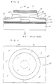
- Figs. 3 and 4 are respectively a cross-sectional view and a plane view of a second embodiment of semiconductor laser device of the invention, which is a surface emission type semiconductor laser device.
- Fig. 1 schematically illustrates a first embodiment of semiconductor laser device according to the invention, which is a quantum well type semiconductor laser device.
- Such a quantum well type semiconductor laser device may typically be prepared in a following manner.
- MOCVD metalorganic chemical vapor deposition
- an SiO2 film is formed on the nondoped InP layer 4 by means of a plasma CVD technique and processed to produce a stripe-shaped stop-etching mask by photolithography.
- the areas not covered by the mask or the lateral sides of the layers from the nondoped InP layer 4 down to the InP semi-insulating substrate 1 are chemically etched to produce a mesa section.
- a p-type InP layer 5, a p-type InGaAsP layer 6 and a semi-insulating InP layer 7 are formed on the lateral sides of or around the mesa section in a second MOCVD process in such a manner that the lateral sides of the mesa section is covered by the p-type InP layer 5 whereas the p-type InGaAsP layer 6 and the semi-insulating InP layer 7 are sequentially formed around the mesa section.
- an n-type InP layer 8 and an n-type InGaAsP layer 9 are sequentially formed on the upper surface of the prepared semiproduct to cover the nondoped InP layer 4 through the p-type InGaAsP layer 6 in a third MOCVD process.
- an n-type electrode 10 is formed on the n-type InGaAsP layer 9 and, as a mesa is formed by chemical etching, using the electrode as a mask, the p-type InGaAsP layer 6 is exposed as a stop-etching layer on the lateral sides, p-type electrodes 11 are formed on the respective surfaces of the layer.
- Fig. 2 shows a graph showing the modulation response of a quantum well type semiconductor laser device according to the invention and obtained by a simulation along with those of a conventional device using a conventional modulation technique.
- ⁇ r is defined by the thickness of the optical confinement layers and the mobility of holes and assumed to be approximately 50 psec.
- a quantum well semiconductor laser device since electrons are injected through the optical confinement layers and the barrier layer into the quantum well layer, while holes are injected directly into the quantum well layer without passing through the optical confinement layers and the barrier layer, the carrier density within the quantum well layer is directly modulated to improve the modulation response of the device.
- Figs. 3 and 4 illustrates a second embodiment of the invention, which is a surface emission type semiconductor laser device.
- Such a surface emission type semiconductor laser device may typically be prepared in a following manner.
- a semi-insulating multilayer film (multilayer reflection film) 42, a p-type doped InP lower clad layer 43, a nondoped InGaAsP active layer 44, a nondoped InP upper clad layer 45 are sequentially formed on a semiconductor InP semi-insulating substrate 1 by epitaxial growth in a first MOCVD process.
- the p-type doped InP lower clad layer 43 is 1 ⁇ m thick and doped with Zn to a concentration of approximately 5x1017cm ⁇ 3.
- the nondoped upper clad layer 45 is 0. 5 ⁇ m thick.
- an SiO2 film is formed on the nondoped InP upper clad layer 45 by plasma CVD technique and processed by photolithography to show a circular form having a diameter of 4 ⁇ m so that it may be used as an etching-resist mask.
- the areas not covered by the mask or the surrounding areas from the nondoped InP layer 45 down to the InP semi-insulating substrate 41 are chemically etched to produce a circular mesa section.
- a p-type InP surrounding lateral layer 46, a p-type InGaAsP contact layer 47 and a semi-insulating InP layer 48 for current confinement are formed on the upper surface and the lateral sides of or around the circular mesa section in a second MOCVD process using the SiO2 film as a mask for selective growth in such a manner that the circular mesa section is covered by these layers.
- the p-type InP surrounding lateral layer 46 is doped with Zn to a concentration of approximately 5x1017cm ⁇ 3.
- the semi-insulating InP layer 48 is doped with Fe.
- an n-type InP layer 49 and an n-type semi-insulating multilayer film (multilayer reflection film) 50 are sequentially formed on the upper surface of the prepared semiproduct to cover the nondoped InP layer 45 through the semi-insulating InP layer 48 in a third organometallic vapor deposition process.
- the n-type InP layer 49 shows a carrier density of approximately 1x1018cm ⁇ 3.
- the n-type semi-insulating multilayer film 50 has a structure substantially same as that of the semi-insulating film 42 except that it has a carrier density of approximately 1x1018cm ⁇ 3 and is doped to n-type.
- an n-type electrode 51 is formed on the n-type semi-insulating multilayer film 50 and, as a circular mesa is formed by chemical etching, using the electrode as a mask, the p-type InGaAsP contact layers 47 is exposed as an etching prohibiting layer, p-type electrodes 52 are formed on the respective surfaces of the p-type InGaAsP contact layer.
- the electric current injected from the p-type electrodes 52 are introduced into the non-doped InGaAsP active layer 44 through its lower surface and the lateral sides by way of the p-type doped lower clad layer 43 and the p-type InP surrounding lateral clad layer 46 without passing through the semi-insulating multi layer film 42.
- the electric current is not only evenly injected into the active layer 44 but also does not lose the high-speed response of the device, because it is confined by the semi-insulating InP layer 48 in the device where the n-type electrode 51 and the p-type electrodes 52 are not oppositely arranged.
- optical output of an above described surface emission type semiconductor laser device is emitted along a direction indicated by an arrow in Fig. 3.
- the hole injection path as disclosed above is applicable to any semiconductor laser devices other than the quantum well and the surface emission types having a configuration different from those of the embodiments provided that an n-type electrode and p-type electrodes are arranged on the upper surface of a semiconductor wafer.
- the semiconductor substrate (semi-insulating substrate) of a semiconductor laser device according to the present invention is not limited to an InP substrate but any other known substrates including GaAs substrates may also appropriately be used.
- the active layer to be used for the purpose of the present invention may be either of a single quantum well type or a multiple quantum well type and the optical confinement layers may have an SCH (Separate Confine Heterostructure) or GIN-SCH (Graded Index-Separate Confinement Heterostructure) structure.
- the remaining layers of a semiconductor laser device according to the present invention may appropriately include III-V group p-type layers containing compound semiconductor alloys, n-type layers, doped layers, nondoped layer and any combinations of them.
- n-type and p-type electrodes to be used for the purpose of the present invention may be appropriately selected from those of any known types.
- a semiconductor laser device comprises a lower optical confinement layer, an active layer and an upper optical confinement layer, said active layer being inserted between said upper and lower optical confinement layers and is characterized in that an electron injection path for injecting electrons into the active layer by way of the optical confinement layers and a hole injection path for injecting holes into the active layer without passing through the optical confinement layers are formed therein, evidently electrons are injected into the active layer by way of the optical confinement layers while holes are directly injected into the active layer without passing through the optical confinement layers to remarkably improve the modulation response and the modulation speed of the device.
- a semiconductor laser device as disclosed by the present invention can be usefully and effectively used as a optical source for optical transmission in the field of optical telecommunications and optical instrumentation because of its high-speed modulation capability.
Landscapes
- Physics & Mathematics (AREA)
- Optics & Photonics (AREA)
- Condensed Matter Physics & Semiconductors (AREA)
- General Physics & Mathematics (AREA)
- Electromagnetism (AREA)
- Chemical & Material Sciences (AREA)
- Engineering & Computer Science (AREA)
- Nanotechnology (AREA)
- Life Sciences & Earth Sciences (AREA)
- Biophysics (AREA)
- Crystallography & Structural Chemistry (AREA)
- Semiconductor Lasers (AREA)
Applications Claiming Priority (2)
| Application Number | Priority Date | Filing Date | Title |
|---|---|---|---|
| JP4105388A JPH05283802A (ja) | 1992-03-31 | 1992-03-31 | 量子井戸半導体レーザ素子 |
| JP105388/92 | 1992-03-31 |
Publications (2)
| Publication Number | Publication Date |
|---|---|
| EP0587911A1 true EP0587911A1 (en) | 1994-03-23 |
| EP0587911A4 EP0587911A4 (enExample) | 1994-08-31 |
Family
ID=14406272
Family Applications (1)
| Application Number | Title | Priority Date | Filing Date |
|---|---|---|---|
| EP93906859A Withdrawn EP0587911A1 (en) | 1992-03-31 | 1993-03-31 | Semiconductor laser device |
Country Status (4)
| Country | Link |
|---|---|
| US (1) | US5544189A (enExample) |
| EP (1) | EP0587911A1 (enExample) |
| JP (1) | JPH05283802A (enExample) |
| WO (1) | WO1993020604A1 (enExample) |
Families Citing this family (3)
| Publication number | Priority date | Publication date | Assignee | Title |
|---|---|---|---|---|
| US5789772A (en) * | 1994-07-15 | 1998-08-04 | The Whitaker Corporation | Semi-insulating surface light emitting devices |
| JP2001085789A (ja) * | 1999-09-13 | 2001-03-30 | Furukawa Electric Co Ltd:The | 面発光型半導体レーザ素子及びその製造方法 |
| TW201409881A (zh) * | 2012-08-16 | 2014-03-01 | jin-wei Xu | 可調控光學模態之垂直共振腔面射型雷射 |
Family Cites Families (8)
| Publication number | Priority date | Publication date | Assignee | Title |
|---|---|---|---|---|
| US4166278A (en) * | 1978-03-29 | 1979-08-28 | Mitsubishi Denki Kabushiki Kaisha | Semiconductor injection laser device |
| JPS6352494A (ja) * | 1986-08-22 | 1988-03-05 | Hitachi Ltd | 光電子装置の製造方法およびモジユ−ル |
| JPS6352495A (ja) * | 1986-08-22 | 1988-03-05 | Omron Tateisi Electronics Co | 半導体発光素子 |
| US4901327A (en) * | 1988-10-24 | 1990-02-13 | General Dynamics Corporation, Electronics Division | Transverse injection surface emitting laser |
| JPH02174286A (ja) * | 1988-12-27 | 1990-07-05 | Mitsubishi Electric Corp | 半導体レーザの製造方法 |
| JP2815165B2 (ja) * | 1989-01-30 | 1998-10-27 | 工業技術院長 | 二方向注入型半導体レーザ装置 |
| JPH0460522A (ja) * | 1990-06-29 | 1992-02-26 | Toshiba Corp | 半導体光増幅器 |
| US5343487A (en) * | 1992-10-01 | 1994-08-30 | Optical Concepts, Inc. | Electrical pumping scheme for vertical-cavity surface-emitting lasers |
-
1992
- 1992-03-31 JP JP4105388A patent/JPH05283802A/ja active Pending
-
1993
- 1993-03-31 WO PCT/JP1993/000405 patent/WO1993020604A1/ja not_active Ceased
- 1993-03-31 EP EP93906859A patent/EP0587911A1/en not_active Withdrawn
- 1993-03-31 US US08/157,099 patent/US5544189A/en not_active Expired - Lifetime
Also Published As
| Publication number | Publication date |
|---|---|
| WO1993020604A1 (fr) | 1993-10-14 |
| EP0587911A4 (enExample) | 1994-08-31 |
| JPH05283802A (ja) | 1993-10-29 |
| US5544189A (en) | 1996-08-06 |
Similar Documents
| Publication | Publication Date | Title |
|---|---|---|
| US6134368A (en) | Optical semiconductor device with a current blocking structure and method for making the same | |
| US5306923A (en) | Optoelectric device with a very low series resistance | |
| EP0488820B1 (en) | Optical semiconductor device | |
| EP0896406A2 (en) | Semiconductor laser device, optical communication system using the same, and method for producing compound semiconductor | |
| US6383829B1 (en) | Optical semiconductor device and method of fabricating the same | |
| CA2007383C (en) | Semiconductor optical device | |
| EP1202410A2 (en) | Semiconductor laser device | |
| US6682949B2 (en) | Semiconductor laser and production method thereof | |
| US5580818A (en) | Fabrication process for semiconductor optical device | |
| US5847415A (en) | Light emitting device having current blocking structure | |
| US8847357B2 (en) | Opto-electronic device | |
| EP0587911A1 (en) | Semiconductor laser device | |
| US6078602A (en) | Separate confinement heterostructured semiconductor laser device having high speed characteristics | |
| Furuya et al. | AlGaAs/GaAs lateral current injection multiquantum well (LCI-MQW) laser using impurity-induced disordering | |
| JP3604400B2 (ja) | 半導体レーザ素子 | |
| US7288783B2 (en) | Optical semiconductor device and method for fabricating the same | |
| JPH08236857A (ja) | 長波長半導体レーザおよびその製造方法 | |
| EP0708997B1 (en) | Electrical barrier structure for semiconductor device | |
| US6967770B2 (en) | Semiconductor optical amplifier with reduced effects of gain saturation | |
| US5539762A (en) | Article comprising a semiconductor laser with carrier stopper layer | |
| JPH01179488A (ja) | 光増幅器 | |
| JPS6237557B2 (enExample) | ||
| JPS6356977A (ja) | 半導体レ−ザ | |
| JP3096667B2 (ja) | 波長可変発光素子 | |
| KR900000021B1 (ko) | 반도체 레이저 |
Legal Events
| Date | Code | Title | Description |
|---|---|---|---|
| PUAI | Public reference made under article 153(3) epc to a published international application that has entered the european phase |
Free format text: ORIGINAL CODE: 0009012 |
|
| AK | Designated contracting states |
Kind code of ref document: A1 Designated state(s): DE FR GB |
|
| 17P | Request for examination filed |
Effective date: 19940411 |
|
| A4 | Supplementary search report drawn up and despatched | ||
| AK | Designated contracting states |
Kind code of ref document: A4 Designated state(s): DE FR GB |
|
| 17Q | First examination report despatched |
Effective date: 19950913 |
|
| STAA | Information on the status of an ep patent application or granted ep patent |
Free format text: STATUS: THE APPLICATION IS DEEMED TO BE WITHDRAWN |
|
| 18D | Application deemed to be withdrawn |
Effective date: 19960326 |