EP0586554B1 - Binärdaten-fehlerkorrektur in einem modulierten signal mit hinweissignal auf vorgegebenen grenzwert überschreitende störgeräusche - Google Patents
Binärdaten-fehlerkorrektur in einem modulierten signal mit hinweissignal auf vorgegebenen grenzwert überschreitende störgeräusche Download PDFInfo
- Publication number
- EP0586554B1 EP0586554B1 EP92912860A EP92912860A EP0586554B1 EP 0586554 B1 EP0586554 B1 EP 0586554B1 EP 92912860 A EP92912860 A EP 92912860A EP 92912860 A EP92912860 A EP 92912860A EP 0586554 B1 EP0586554 B1 EP 0586554B1
- Authority
- EP
- European Patent Office
- Prior art keywords
- signal
- noise
- bits
- error
- output
- Prior art date
- Legal status (The legal status is an assumption and is not a legal conclusion. Google has not performed a legal analysis and makes no representation as to the accuracy of the status listed.)
- Expired - Lifetime
Links
Images


Classifications
-
- H—ELECTRICITY
- H04—ELECTRIC COMMUNICATION TECHNIQUE
- H04L—TRANSMISSION OF DIGITAL INFORMATION, e.g. TELEGRAPHIC COMMUNICATION
- H04L1/00—Arrangements for detecting or preventing errors in the information received
- H04L1/004—Arrangements for detecting or preventing errors in the information received by using forward error control
- H04L1/0056—Systems characterized by the type of code used
- H04L1/0057—Block codes
-
- G—PHYSICS
- G06—COMPUTING OR CALCULATING; COUNTING
- G06F—ELECTRIC DIGITAL DATA PROCESSING
- G06F11/00—Error detection; Error correction; Monitoring
- G06F11/07—Responding to the occurrence of a fault, e.g. fault tolerance
- G06F11/08—Error detection or correction by redundancy in data representation, e.g. by using checking codes
- G06F11/10—Adding special bits or symbols to the coded information, e.g. parity check, casting out 9's or 11's
-
- H—ELECTRICITY
- H03—ELECTRONIC CIRCUITRY
- H03M—CODING; DECODING; CODE CONVERSION IN GENERAL
- H03M13/00—Coding, decoding or code conversion, for error detection or error correction; Coding theory basic assumptions; Coding bounds; Error probability evaluation methods; Channel models; Simulation or testing of codes
- H03M13/03—Error detection or forward error correction by redundancy in data representation, i.e. code words containing more digits than the source words
- H03M13/05—Error detection or forward error correction by redundancy in data representation, i.e. code words containing more digits than the source words using block codes, i.e. a predetermined number of check bits joined to a predetermined number of information bits
- H03M13/09—Error detection only, e.g. using cyclic redundancy check [CRC] codes or single parity bit
- H03M13/098—Error detection only, e.g. using cyclic redundancy check [CRC] codes or single parity bit using single parity bit
-
- H—ELECTRICITY
- H03—ELECTRONIC CIRCUITRY
- H03M—CODING; DECODING; CODE CONVERSION IN GENERAL
- H03M13/00—Coding, decoding or code conversion, for error detection or error correction; Coding theory basic assumptions; Coding bounds; Error probability evaluation methods; Channel models; Simulation or testing of codes
- H03M13/03—Error detection or forward error correction by redundancy in data representation, i.e. code words containing more digits than the source words
- H03M13/05—Error detection or forward error correction by redundancy in data representation, i.e. code words containing more digits than the source words using block codes, i.e. a predetermined number of check bits joined to a predetermined number of information bits
- H03M13/13—Linear codes
- H03M13/15—Cyclic codes, i.e. cyclic shifts of codewords produce other codewords, e.g. codes defined by a generator polynomial, Bose-Chaudhuri-Hocquenghem [BCH] codes
- H03M13/151—Cyclic codes, i.e. cyclic shifts of codewords produce other codewords, e.g. codes defined by a generator polynomial, Bose-Chaudhuri-Hocquenghem [BCH] codes using error location or error correction polynomials
-
- H—ELECTRICITY
- H03—ELECTRONIC CIRCUITRY
- H03M—CODING; DECODING; CODE CONVERSION IN GENERAL
- H03M13/00—Coding, decoding or code conversion, for error detection or error correction; Coding theory basic assumptions; Coding bounds; Error probability evaluation methods; Channel models; Simulation or testing of codes
- H03M13/03—Error detection or forward error correction by redundancy in data representation, i.e. code words containing more digits than the source words
- H03M13/05—Error detection or forward error correction by redundancy in data representation, i.e. code words containing more digits than the source words using block codes, i.e. a predetermined number of check bits joined to a predetermined number of information bits
- H03M13/13—Linear codes
- H03M13/19—Single error correction without using particular properties of the cyclic codes, e.g. Hamming codes, extended or generalised Hamming codes
-
- H—ELECTRICITY
- H03—ELECTRONIC CIRCUITRY
- H03M—CODING; DECODING; CODE CONVERSION IN GENERAL
- H03M13/00—Coding, decoding or code conversion, for error detection or error correction; Coding theory basic assumptions; Coding bounds; Error probability evaluation methods; Channel models; Simulation or testing of codes
- H03M13/25—Error detection or forward error correction by signal space coding, i.e. adding redundancy in the signal constellation, e.g. Trellis Coded Modulation [TCM]
- H03M13/251—Error detection or forward error correction by signal space coding, i.e. adding redundancy in the signal constellation, e.g. Trellis Coded Modulation [TCM] with block coding
-
- H—ELECTRICITY
- H04—ELECTRIC COMMUNICATION TECHNIQUE
- H04B—TRANSMISSION
- H04B3/00—Line transmission systems
- H04B3/54—Systems for transmission via power distribution lines
- H04B3/542—Systems for transmission via power distribution lines the information being in digital form
-
- H—ELECTRICITY
- H04—ELECTRIC COMMUNICATION TECHNIQUE
- H04L—TRANSMISSION OF DIGITAL INFORMATION, e.g. TELEGRAPHIC COMMUNICATION
- H04L1/00—Arrangements for detecting or preventing errors in the information received
- H04L1/22—Arrangements for detecting or preventing errors in the information received using redundant apparatus to increase reliability
-
- H—ELECTRICITY
- H04—ELECTRIC COMMUNICATION TECHNIQUE
- H04B—TRANSMISSION
- H04B2203/00—Indexing scheme relating to line transmission systems
- H04B2203/54—Aspects of powerline communications not already covered by H04B3/54 and its subgroups
- H04B2203/5404—Methods of transmitting or receiving signals via power distribution lines
- H04B2203/5408—Methods of transmitting or receiving signals via power distribution lines using protocols
-
- H—ELECTRICITY
- H04—ELECTRIC COMMUNICATION TECHNIQUE
- H04B—TRANSMISSION
- H04B2203/00—Indexing scheme relating to line transmission systems
- H04B2203/54—Aspects of powerline communications not already covered by H04B3/54 and its subgroups
- H04B2203/5404—Methods of transmitting or receiving signals via power distribution lines
- H04B2203/5416—Methods of transmitting or receiving signals via power distribution lines by adding signals to the wave form of the power source
-
- H—ELECTRICITY
- H04—ELECTRIC COMMUNICATION TECHNIQUE
- H04B—TRANSMISSION
- H04B2203/00—Indexing scheme relating to line transmission systems
- H04B2203/54—Aspects of powerline communications not already covered by H04B3/54 and its subgroups
- H04B2203/5404—Methods of transmitting or receiving signals via power distribution lines
- H04B2203/5425—Methods of transmitting or receiving signals via power distribution lines improving S/N by matching impedance, noise reduction, gain control
-
- H—ELECTRICITY
- H04—ELECTRIC COMMUNICATION TECHNIQUE
- H04B—TRANSMISSION
- H04B2203/00—Indexing scheme relating to line transmission systems
- H04B2203/54—Aspects of powerline communications not already covered by H04B3/54 and its subgroups
- H04B2203/5429—Applications for powerline communications
- H04B2203/5445—Local network
-
- H—ELECTRICITY
- H04—ELECTRIC COMMUNICATION TECHNIQUE
- H04B—TRANSMISSION
- H04B2203/00—Indexing scheme relating to line transmission systems
- H04B2203/54—Aspects of powerline communications not already covered by H04B3/54 and its subgroups
- H04B2203/5462—Systems for power line communications
- H04B2203/5483—Systems for power line communications using coupling circuits
-
- H—ELECTRICITY
- H04—ELECTRIC COMMUNICATION TECHNIQUE
- H04B—TRANSMISSION
- H04B2203/00—Indexing scheme relating to line transmission systems
- H04B2203/54—Aspects of powerline communications not already covered by H04B3/54 and its subgroups
- H04B2203/5462—Systems for power line communications
- H04B2203/5491—Systems for power line communications using filtering and bypassing
-
- H—ELECTRICITY
- H04—ELECTRIC COMMUNICATION TECHNIQUE
- H04B—TRANSMISSION
- H04B2203/00—Indexing scheme relating to line transmission systems
- H04B2203/54—Aspects of powerline communications not already covered by H04B3/54 and its subgroups
- H04B2203/5462—Systems for power line communications
- H04B2203/5495—Systems for power line communications having measurements and testing channel
Definitions
- the invention relates to the field of power line communications and, more particularly, transceivers enabling such communications.
- U.S. Patent No. 4,918,690 describes a system for providing sensing bidirectional communications and control. Communications between a plurality of cells enables, for example, control for switching and the like.
- the present invention provides a transceiver for power line communications which may be used with the system described in U.S. Patent No. 4,918,690.
- a major problem with power line communications is background noise including impulse noise.
- This noise originates not only from the power source and distribution network, but also from the loads.
- the noise is not constant with respect to time and moreover, it varies from place to place in a power distribution network.
- a theoretical analysis of impulse noise, particularly for a twisted pair is described in "Errors-and-Erasures Coding to Combat Impulse Noise on Digital Subscriber Loops", IEEE Transactions on Communications, Vol. 38, No. 8, August 1990, beginning at page 1145.
- the present invention employs snubbing or blanking to eradicate noise impulses. Applicant is not aware of this technique being applied to a digital system. Snubbing or blanking has been used in connection with radio receivers and its use is described in U.S. Patent No. 4,124,819.
- X-10 One commercially available system "X-10" provides sensing, control and communications over power lines. Coded patterns are transmitted twice, once in true form and a second time in complementary form on a modulated carrier. This technique provides only limited immunity to power line noise.
- the carrier detection threshold level is fixed. In selecting a threshold level for such a system, the level must be relatively high to provide some immunity from expected noise. This limits the operation of the system, for instance, where both the noise and signal are low.
- the present invention provides an adaptive carrier detection level.
- the present invention uses two channels, however, selection between one or the other (or both) channels is based on noise levels, not signal strength.
- ECC error correcting codes
- Hamming codes such as Hamming codes
- a method as claimed in claim 1 is described for detecting and correcting errors in a signal representing binary data.
- the signal is examined for anomalies, for example by detecting noise pulses which exceed certain limits.
- the datum that occurred in the binary data at the point where the noise pulse occurred is identified by a "hint" signal. This datum is subjected to verification.
- data is encoded using a (15, 11) Hamming code and a parity bit. Double errors, when detected, are corrected by using the Hamming code and by changing the state of the binary signal pointed to by the hint signal.
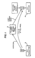
- Figure 1 is a diagram used to illustrate problems associating with power line communications.
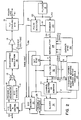
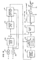
- FIG. 2 is a block diagram of the invented power line communications apparatus.
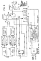
- Figure 3 is a block diagram of the pulse detector and snubber of Figure 2.
- Figure 4 illustrates several waveforms used to explain the operation of the pulse detector and snubber of Figure 3.
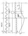
- Figure 5 illustrates several waveforms used to describe the effect of snubbing on a modulated carrier.
- Figure 6 illustrates the flow of data, Hamming code, and a parity bit in the present invention.
- Figure 7 is a diagram illustrating the implementation of a Hamming code in the present invention.
- Figure 8 is a circuit diagram of the snub hint generator of the present invention.
- FIG. 9 illustrates several waveforms used to explain the operation of the circuit of Figure 8.
- Figure 10 is a state diagram used to describe the mechanism for updating the carrier detection threshold level.
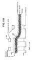
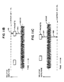
- Figure 11a illustrates a plurality of waveforms used to describe the condition when the carrier detection threshold level is above the average noise level.
- Figure 11b illustrates a plurality of waveforms used to describe the condition when the carrier detection threshold level is above the level of the carrier signal.
- Figure 11c illustrates a plurality of waveforms used to describe the condition when the carrier detection threshold level is below the noise level.
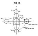
- Figure 12 is a diagram used to describe the locations of data constellations for a quadrature modulated signal.
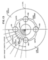
- Figure 13 is a graph similar to that of Figure 12 used to indicate the target areas where data should be located.
- Figure 14 is a block diagram of the currently preferred embodiment of a portion of the adaptive carrier detection circuit.
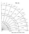
- Figure 15 is a graph illustrating the coefficient values used in the score table of Figure 14.
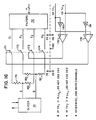
- Figure 16 is a circuit diagram of the channel selection or addition circuit of Figure 2.
- Figure 17 is a graph of the characteristics of a filter used in the pulse detector of Figure 2.
- a power line communication (PLC) apparatus which enables communications over power lines between cells or other devices.
- the apparatus may be realized either with discrete components or as an integrated circuit formed on a single substrate employing well-known complimentary metal-oxide-semiconductor (CMOS) technology or other semiconductor processing technologies.
- CMOS complimentary metal-oxide-semiconductor
- the power lines referred to are typically used to distribute 50 or 60Hz A.C. power, although in some cases higher frequencies are used such as 400Hz in aircraft or lower frequencies such as 25Hz in some rail systems.
- the power line communication signals are transmitted over the same lines that carry the power by modulating a higher frequency carrier signal. For instance, a 150kHz carrier may be used to communicate digital signals over the power lines at a baud rate of 10kB.
- a power line communication transmitter 8 is illustrated connected into a typical household electrical receptacle.
- the transmitter 8 may be embedded within the receptacle to control another outlet.
- the transmitter 8 transmits signals to a PLC receiver 10 which controls an appliance coupled into the receptacle associated with receiver 10.
- the communications path between the transmitter 8 and receiver 10, as illustrated, passes through a circuit breaker panel. This is often the case where one of the receptacles is on one branch circuit and the other on another branch circuit.
- a signal transmitted by transmitter 8 at, for example, 150kHz may be attenuated by more than 40dB before reaching the receiver 10.
- the transmitter 8 is transmitting with a one volt output, the voltage at receiver 10 will be substantially diminished.
- noise and other transients associated with power lines distribution system that make it difficult to receive and/or reconstruct signals from a PLC transmitter.
- One source of noise is an electronic dimmer which "chops" the A.C. waveform.
- Another example of noise is a switching power supply, frequently used in personal computers, which produce high frequency noise bursts (e.g., 25kHz or greater).
- Other sources of noise found in a home or commercial environment include intercoms, electric motors, televisions and numerous others. Consequently, the receiver 10 must be able to ferret out the communications signal from the noise on the power line. (although in the above discussion, a separate transmitter and receiver are shown, typically the functions of transmitting and receiving are combined into a single device.)
- the transmit section of the PLC apparatus while the lower portion of Figure 2 is the receive section.
- the transmit section is included here for clarity.
- the transmit section is not the subject of the present invention.
- This latter section receives signals over the power line 41, processes them, then couples the resultant digital signal to the I/O buffer and control circuit 10. From there, the signals are coupled over lines 40 to a cell or other device.
- the data to be transmitted which arrives from the cell over lines 40 is coupled to an error correcting code encoder 11.
- the data is encoded, in the currently preferred embodiment, with a (15,11) Hamming code, meaning that 4 bits of error correction code are appended to each 11 bit data word.
- the encoding may be done in an ordinary manner, however, since 8-bit data words are encoded, means are provided for incorporating "dummy" or placeholder bits with each byte both during encoding and decoding as will be described in conjunction with Figure 6.
- a parity bit is also transmitted with each word.
- Data is transmitted from the cell onto the power line in packets with the preamble generator 12 providing a preamble for the packets.
- the preamble is positioned in front of the packets of encoded data from the encoder 11. Consequently, the summer 13 performs a multiplexing function in that it selects either the data or preamble.
- the output of the summer 13 is coupled to a waveshaping and modulating circuit 14.
- this circuit includes a read-only-memory, digital-to-analog converter and two filters. (The filters in the integrated circuit embodiment of the present invention are switched capacitor filters.)
- the data is transmitted in its entirety on two channels, that is, there is redundancy in the transmission. All the data (including the preamble) modulates both a 118kHz carrier and a 133.7kHz carrier for PLC apparatuses designed for use in the United States. (Other carrier frequencies are used for other countries to comply with different regulations.) The frequency separation between the frequencies is discussed in conjunction with the channel selection or addition circuit 33 of Figure 16. While the data is transmitted on both channels, the receiver selects one or both channels, as will be described.
- Quadrature phase shift keying is used to modulate the carriers under most operations.
- BPSK is also used as described in the above mentioned applications.
- BPSK signaling at half the bit rate of QPSK signaling, is more immune to noise than QPSK but slower.
- the BPSK signaling scheme has the same receiver structure as QPSK, but uses only a two-point subset of the four-point QPSK signaling constellation.
- the BPSK signaling scheme communicates one bit of digital information in every signaling baud period. (Date bit rate and baud rate are equal.)
- the QPSK signaling scheme communicates two bits of digital information in every signaling baud period (data bit rate is twice the baud rate).
- the signaling baud rates for BPSK and QPSK signaling determined by physical parameters of the receiver filters are the same. In some of the examples below BPSK is discussed since it is easier to understand of the present invention when the bit rate is equal to the baud rate.
- the output of the waveshaping and modulation circuit 14 is coupled to an amplifier 15 and from there to the power line 41 through a power line coupling network 16.
- the amplifier 15 and network 16 are fabricated from discrete components.
- Filters 18 again comprise switched capacitor filters for the integrated circuit embodiment.
- the filters 18 comprise a high pass filter and a low pass filter.
- the high pass filter has a cut-off frequency of approximately 90-110kHz, and the low pass filter, a cut-off frequency of approximately 320kHz.
- the filters 18 thus pass the modulated carriers and additionally the filters 18 pass certain noise.
- the pulse detector 20 receives the output of the filters 18 (node 42).
- the detector 20 detects anomalies in the waveform such as noise pulses or other excursions of the waveform above or below certain threshold levels. For example, the pulse detector 20 detects noise associated with a light dimmer and other sources of noise pulses.
- the pulse detector 20 provides a snubber control signal to a snubber 22 on line 61.
- the snubber 22 blanks or snubs the signals from filters 18 for predetermined periods when a pulse representing a disturbance (noise pulse) is present in the received signal.
- the pulse detector 20 and snubber 22 are described in conjunction with Figure 3.
- the output of the snubber 22 which is the main received signal path is coupled to demodulation 28 on line 64.
- the carrier synchronization circuit 26 provides COS ⁇ c1, SIN ⁇ c1, COS ⁇ c2 and SIN ⁇ c2 to the demodulator 28.
- Four signals are coupled from the demodulator 28 to the circuit 26 (two for each channel). As mentioned above, two carriers are used and hence two channels are needed; one for the 118kHz signal and the other for the 133.7kHz signal.
- the demodulator 28 under control of the output of detector 26, demodulates the two carrier signals and provides both an in-phase and quadrature phase signal for each of the two channels to the filters 32.
- the output of the demodulator 28 is also coupled to a bit (baud) synchronization circuit 30.
- This circuit provides baud synchronization to the decoder 34 as well as other circuits.
- Circuit 30 also provides snub frame timing signals shown in Figure 9 and elsewhere.
- the demodulator 28 and bit synchronization circuit 30 are ordinary, well-known circuits except as discussed herein.
- the two channel carrier detect and adaptive carrier detect threshold circuit 29 uses an adaptive threshold level which is described in conjunction with Figures 10-15.
- the filters 32 comprise four matched filters, two for each channel. These filters may be of ordinary design for the illustrated use.
- the output of the filters 32 are coupled to the channel selection or addition circuit 33.
- This circuit receives two control (selection) signals from the circuit 29.
- the data from one channel or the other from filters 32 is selected and forwarded to the bit slicer 31, or the data in both channels is added together and forwarded to the bit slicer 31. (Note: the same data is present in both channels.)
- the noise in one channel is high, relative to noise in the other channel, the channel with the lesser noise is selected. If the noise is both channels is approximately equal, the signals in the channels are added. Details of this circuit are described in conjunction with Figure 16.
- the output from circuit 33 is coupled to the slicer 31 where the waveform is converted to a digital form in an ordinary manner under control of the bit synchronization signal.
- the output of circuit 33 is shown by the waveform on line 96 of Figure 5.
- the slicer 31 provides the binary 1 or 0 levels by detecting the signal level at, for example, time 100. (This diagram shows BPSK for purposes of explanation. In the QPSK case two signals are forwarded from the channel selection circuit 33 to the slicer 31 and the slicer outputs two bits per signaling baud.)
- the signal from slicer 31 is coupled to the preamble decoder 35 where the preamble is stripped off.
- the output of decoder 35 is coupled to the ECC decoder 34.
- One novelty of the present invention is the use of a "hint" from the pulse detector 20 which permits correction of a second transmission error in each byte under certain conditions.
- the position along the modulated waveform where an unsnubbed noise pulse occurs provides the hint as to where an error may have occurred in the data.
- a hint signal is transmitted on line 36 to the decoder 34 allowing the decoder to know where in the data stream the noise pulse occurred, and thus, where it is likely that an error may have occurred.
- the use of the hint in connection with the decoder 34 is described in conjunction with Figures 3 through 9.
- the decoded data is coupled from the decoder 34 to the input/output buffer and control circuit 10 and from there to the cell or other device over lines 40.
- DSP digital signal processing
- FIG 3 the pulse detector 20 and snubber 22 of Figure 2 are shown in detail.
- the input to the snubber 22 of Figure 2 (node 43), is shown in Figure 3 on the right edge of the figure.
- Node 43 is coupled to a delay circuit 73 to delay the modulated carriers for reasons which will be explained.
- the delayed signal is the output signal on line 64.
- This signal is snubbed through an analog switch 63; that is, the received signal (carriers and noise pulses) are selectively blanked under control of the snub control (SNUBCTL) signal which signal operates the switch 63.
- SNUBCTL snub control
- the input to the pulse detector 20 (node 42) of Figure 2 is shown in the upper left comer of Figure 3.
- Node 42 is coupled to the inputs of filters 44 and 45.
- the high pass filter 44 has a cut-off frequency of approximately 150kHz hence, the output of filter 44 consists approximately of the band 150-320kHz (this band excludes the carriers).
- the output of the filter 44 is coupled to a positive envelope detector 47 and a negative envelope detector 48. Also, this filters output is coupled directly to a window comparator 53.
- the outputs of the positive and negative envelope detectors provide envelope threshold signals which are proportional to the background noise. Signals at the output of the filter 44 which are greater than the envelopes by a certain amount (either in the positive or negative sense) are detected within the window comparator 53.
- a signal occurs at the output of comparator 53 whenever the output of the filter 44 exceeds by the certain amount the threshold levels established by either the positive or negative envelope detectors.
- the positive and negative envelope detectors along with the window comparator as a full wave rectifier with a threshold level established by the background signal. What is occurring is that the threshold levels are established by the noise; pulses which are greater than the established threshold levels are detected and provided an output to one terminal of OR gate 56.
- the detectors 47 and 48 have an approximately 850 microsecond charging time constant and a 6.8 millisecond discharging time constant; detectors 50 and 51 have an approximately 150 microsecond charging time constant and a 300 microsecond discharging time constant.
- the low pass notch filter 45 in the currently preferred embodiment, provides a low pass filter which significantly attenuates (25dB or greater) signals above 200kHz. The reason for this filter will be described shortly.
- the output of filter 45 is processed in a similar manner to the output of filter 44. Specifically, filter 45's output is coupled to a positive envelope detector 50, a negative envelope detector 51 and a window comparator 54. Once again, pulses exceeding the threshold levels established by detectors 50 and 51 by the certain amount, produce signals from comparator 54; these signals are coupled to the other terminal of the OR gate 56. However, in this case the carrier signal of received packets set the threshold levels.
- the pulse detector is to blank the modulated carriers when a noise pulse occurs, it would seem that the output of window comparator 53 is all that is needed. It has been found however, that continuous interference may occur at 200-400kHz since this is the carrier frequency range associated with some power line intercoms. If an intercom is in use, pulses occurring at 200kHz and above, raise the threshold levels established by detectors 47 and 48, substantially preventing the detection of any noise pulses.
- the circuit of Figure 3 is adaptive in that it compensates for the existence of the intercom disturbance at 200kHz or above.
- the intercom signals as shown by Figure 17, are significantly attenuated by the filter 45.
- the threshold levels established by the detectors 50 and 51 are primarily set by the signals below 200kHz. Consequently, when the intercom signal is present, the output of comparator 54 substantially controls the snubbing through the OR gate 56. This is less desirable than using the output of comparator 53, but is a substantial improvement over losing all snubbing during the presence of the intercom signal.
- this threshold level is high. For this case, noise exceeding (by a factor of 4) the threshold levels established by the carrier signals in comparator 54 is detected.
- the output of the OR gate 56 (SNUBTRY) is coupled to one input terminal of an AND gate 57.
- the output of the AND gate is coupled to the RST terminal of a flip-flop 59.
- the Q/output of this flip-flop is the snub control (SNUBCTL) signal on line 61.
- the S terminal of flip-flop 59 is coupled to the output of a counter 67 through line 72.
- the clock terminal of the flip-flop 59 receives a high frequency (higher than the baud rate) clocking signal. The clocking signal is used throughout the apparatus and is not shown in Figure 2.
- the flip-flop 59 is used to extend the period of the signals from gate 56.
- two pulses 80 and 81 are shown on line 74 which, for purposes of explanation, are assumed to be noise (the modulated carrier is not shown in this drawing).
- a typical pulse includes ringing and thus there is a tail extending from the main source of energy.
- waveform 82 should be used to snub the pulse 80.
- Line 76 illustrates the output of the gate 56. This output has a main pulse 84 associated with the peak level of the noise pulse and one or more additional pulses 85 that occur if the tail of the noise is detected.
- the width is selectable in the range from 30 to 45 microseconds.
- the 30 to 45 microsecond period is not sufficiently long when compared to the baud rate to disturb the detection of a bit or bits which is partially snubbed with one SNUBCTL signal.
- the input to the S terminal of the flip-flop 59 (line 72) determines when SNUBCTL ends; this input is provided by the counter 67.
- the counter 67 receives a 5-bit word from the multiplexer 66. These bits designate one of four times (30, 35, 40 or 45 microseconds). Two bits received from the cell selected one of the four times. An additional signal is used to indicate whether the apparatus is to be used in the United States or Europe to adjust the five bit value due to different clock frequencies.
- the five bit output of the multiplexer 66 is coupled to the counter 67. Counter 67 is enabled and reset when the Q/output from flip-flop 59 goes high; this output is coupled through a rising edge detector 70. Counting occurs under control of a clock signal.
- the main clock signal which is relatively fast, is divided down by the divider 69 before being coupled to the counter 67.
- the period of the counting is a function of the five bit input from MUX 66. Once a predetermined count is reached in the counter 67, a signal on line 72 sets the flip-flop 59, ending the snubbing. In this way, the duration of the snubbing pulses are user selected as 30, 35, 40 or 45 microseconds. (One of these periods may be used as a default period if no selection signals are received by the multiplexer 66.)
- the SNUBCTL signal will not be in time coincidence with the beginning of the noise pulse because of delays in the filters 44 or 45 and other circuits. This is shown on line 76 of Figure 4 by time 83. To compensate for this, the modulated carriers, along with the embedded unwanted noise pulses, are delayed by the delay circuit 73. The delayed noise pulses are shown on line 78 of Figure 4. Line 79 again illustrates the SNUBCTL signal and as can be seen, snubbing occurs in time coincidence with the beginning of the pulse 80 of line 78.
- each SNUBCTL pulse results in a hold-off period of a fixed duration during which another SNUBCTL pulse is prohibited.
- This fixed duration measured from the beginning of the SNUBCTL pulse in the currently preferred embodiment, is approximately 100 microseconds. This period is shown in Figure 4.
- FIG. 5 the effect of the snubbing on a received signal is illustrated for a BPSK case.
- a single noise pulse is shown on line 92 which is assumed to occur with a carrier.
- Waveform 93 shows the modulated carrier during two baud intervals; the first baud interval is modulated with a binary 0 and the second baud interval is modulated with a binary 1. (Note the phase shift in the carrier between the first and second baud time.)
- Line 94 illustrates the SNUBCTL signal generated as described above.
- On line 95 the effect of the snubbing signal on the demodulation signal is shown. During the period 99 there is no signal to detect because the carrier signal is interrupted by the switch 63 of Figure 3.
- the detected signal is illustrated on line 96 at the output of filters 32.
- the binary 0 is detected at time 100 by the slicer 31.
- the binary 1 following this binary 0 should cause the signal to follow the waveform indicated by the dotted line 97, assuming no disturbance occurred and no snubbing occurred.
- the actual waveform on line 96 falls short of its expected amplitude by the amount 98. Nonetheless, a binary 1 is detectable since the voltage represented by 98 is relatively small compared to the total magnitude of the waveform 97. If, on the other hand, a hold-off period was not implemented, additional energy may be lost from the modulated signal from more snubbing, and the binary 1 may not be detectable.
- two or more snubbing pulses may be used during a single frame in some systems.
- the relative amplitudes shown in Figure 5 are for purposes of explanation and are not necessarily representative of actual amplitude.
- the amplitude of the disturbance causing pulse is often much larger than the modulated carriers. This is particularly true for the examples set out in Figure 1 where the transmitter is far from the receiver and the source of the noise close to the receiver.
- the energy associated with the disturbance pulses is often sufficiently large (if not snubbed) to prevent the correct detection of the binary data.
- the snub hint generator includes an AND gate 112; the output of this gate is coupled to the reset terminal of the flip-flop 113.
- the Q/ output of the flip-flop 113 is coupled to the D input of the flip-flop 114.
- the Q output of flip-flop 114 is coupled to the D terminal of the flip-flop 115.
- the Q output of flip-flop 118 provides the snub hint on line 36 of Figure 2.
- the inputs from Figure 3 to the AND gate 115 are the SNUBTRY signal, the SNUBCTL signal (line 61) which is coupled to an inverting terminal and the SNUBENABLE signal which is also coupled to an inverting terminal.
- the SNUBFRAME signal is coupled to the S terminal of the flip-flop 113 and the CE terminal of the flip-flop 114.
- the main clock from Figure 3 is coupled to the clock terminals of flip-flops 113 and 114.
- the baud clock from Figure 3 is coupled to the flip-flop 115.
- the flip-flop 113 in essence, provides an asynchronous reset controlled by the output of gate 112.
- the flip-flops 114 and 115 resynchronize the hint signal to bring it into the baud boundary so that it can be used by the ECC decoder.
- the top waveform illustrates received signal at the snub switch; two bits for data X and Y are used for purposes of explanation.
- the relationship between the baud clock and snub frame signal is shown in Figure 9.
- the SNUBFRAME signal is coupled from the bit synchronization circuit 30 of Figure 2 to the snubber 22. As can be seen, the SNUBFRAME signals occur before each baud clock.
- the SNUBTRY waveform (the output of the OR gate 56 of Figure 3) indicates that during the X frame two disturbances are detected as indicated by the pulses 117 and 118. When the first pulse occurs, the SNUBENABLE signal (output of flip-flop 60 of Figure 3) drops in potential as indicated at the trailing edge 119 of the enable signal.
- a SNUBCTL signal (line 60 of Figure 3) is generated as indicated in Figure 9.
- the flip-flop 113 With the second SNUBTRY pulse 118, the flip-flop 113 is reset and line 120 rises in potential.
- the output of flip-flop 113 is clocked into the flip-flop 114 as indicated by the waveform in Figure 9.
- the flip-flop 115 synchronizes the output of flip-flop 114 with the baud clock, thereby providing the snub hint for the frame X.
- data received at the ECC decoder for frame X occurs at the same time as the snub hint for frame X.
- the encoder 11 encodes data with a Hamming code and a decoder 34 decodes the data.
- the output of a cell 100 is illustrated by an 8-bit digital word 104. These 8 bits are transmitted to a power line communications apparatus 101 such as shown in Figure 2. Once received, three bits 105 are attached to, or placed within, the 8-bit word. The bits 011 become the most significant three bits in an 11-bit data word. These bits are placeholder or dummy bits and are only used to permit use of an available (15,11) Hamming code. This Hamming code operates on 11-bit words and provides a four bit Hamming section. The four bits can detect and correct a single error in the 11 bits.
- the 11 bits comprising the 8-bit word (the real data) and the three placeholder bits are encoded through encoder 109 employing the well-known (15, 11) Hamming code. This results in 15 bits: three placeholder bits, the data (8 bits), and the 4-bit Hamming code 106. Additionally, a parity bit 107 is added to supplement the Hamming code, thereby providing detecting (but not correction) of double bit errors. Before data is transmitted onto the receiver 102, the three placeholder bits are stripped from the word. Thus, only 13 bits are transmitted.
- the particular placeholder bits (011) are selected to maximize the number of transitions (and minimize D.C. drift) in the coded output sequence.
- the same 3 bit code as the previously used for placeholder bits are again placed in the same position in the word. That is, for the example used, 011 shown as three bits 108 become the most significant three bits of an 11-bit data word. All the transceivers in a given system, of course, must use the same placeholder bits and place them in the same relative position prior to encoding and decoding.
- the ordinary Hamming decoder 110 can operate upon the 11 bit data word and the four Hamming code bits in an ordinary manner.
- the output of the decoder 110 includes the three placeholder bits which are stripped from the word.
- the Hamming code and parity bits also are not needed after decoding, therefore, only the 8-bit word is transmitted to the cell 103. (Note: Other parity bits or other encoding may be used between the cells and their respective transceivers independent of the Hamming code and parity bit used between the transceivers.)
- the encoder 11 includes means for adding the three placeholder bits for calculating the Hamming code, and means for removing the placeholder bits prior to the summation that occurs at summer 13.
- the decoder 34 includes means for adding the three placeholder bits prior to decoding, and means for removing the placeholder bits after decoding and prior to coupling the data to the I/O buffer and control circuit 10.
- QSPK encoder 11 interlaces the 13 coded bits from two words. (If the bits in the two words are numbered consecutively 1-26, the bits in the interlaced words are 1, 13, 2, 14, 3, 15).
- the decoder 34 "de-interlaces" the words into their original, non-interlaced order. Consequently, for example, the "01" state represents a "0" in one word and a "1" in the next word. The reason this is done is to avoid having the loss of data for one baud period causing two errors in one word. Rather, the loss is associated with two words. This gives the Hamming code a better chance at correcting infrequent single errors. Also a "hint" for a particular baud period applies to two bits, one in each word for this interlacing.
- the (15, 11) Hamming code permits the detection and correction of a single error per word, as mentioned.
- a parity bit as used in the currently preferred embodiment, a second error can be detected in each word.
- the second error cannot be corrected without other coding.
- the hint on line 36 of Figure 2 is used along with the parity bit to correct a second error, if one occurs.
- an ordinary circuit within decoder 34 examines the data (with the placeholder bits) and the Hamming code bits to determine if an error is present in the word. Also the data is checked to determine if the parity is correct. This is shown by Hamming and parity check in block 112. Block 113 illustrates what occurs if both the Hamming and parity checks indicate that the data is correct. In this instance, it is assumed that the data word is correct. For this case, even if a hint is available for one or more bits in the word, it is ignored since it is assumed that the pulse generating the hint did not corrupt the binary data.
- block 118 shows the case where the Hamming check is bad and the parity check is good. Under these conditions, there must be an even number of errors; it is assumed that there are two errors.
- the hint is used. If there is no hint, the data is not changed. (Higher levels of protocol deal with these errors - for example a cyclic redundancy code (CRC) is used.) If there is one or more hints, then one of the bits associated with a hint signal is inverted. It is now assumed that there is only a single error. The Hamming code is used to correct the remaining error (block 120). If the hint points to the parity bit, after correcting the parity bit, both the Hamming check and parity check will be bad.
- CRC cyclic redundancy code
- one of the hints may be used.
- Other uses of more than one hint are possible, for example, if two hints are generated both hints could be used for certain coding that detects and corrects multiple errors.
- the detection of noise pulses is used to generate the hint signal.
- the hint signal may be generated where other means are used to identify anomalies in the waveform. For instance, in a phase lock loop, frequently used in the demodulation process, abrupt changes in phase in the loop can be detected and used to generate a hint signal. Alternately, the snubbing signal itself may be used to generate the hint signal. Note from Figure 5, waveform 96, that once snubbing occurs the noise margin decreases as indicated by the difference between the expected waveform 97 and the actual waveform 98. Consequently, there is a greater likelihood that a misdetection will occur for a snubbed signal.
- the hint signal can be generated for datum which is snubbed.
- the hint signal may be used in ways different than that described above to verify the data.
- each byte can be transmitted twice with each transmission occurring at a different time. The received redundant bytes can then be compared. If they are the same, it can be assumed the data is correct. On the other hand, if there is a mismatch, and a hint signal is generated, the state of the bit associated with the hint signal can be changed and the bytes again compared to see of the suspected error is corrected.
- the two channel carrier detect and adaptive carrier detect threshold circuit 29 includes a carrier detect mechanism having two sections; one for each channel. This mechanism uses well-known principles and for this reason it is not set forth in detail. This is also true for the carrier synchronization circuit 26. What is novel, however, is the adaptive carrier detection threshold level; it automatically changes level depending on noise conditions. This adaptive carrier detection threshold level is generated within circuit 29 of Figure 2. In summary, this adaptive threshold is generated using unsupervised learning implemented by the equations shown in Figure 10 and data quality estimator the specific coefficients of which are shown in Figure 15.
- circuitry is employed to generate an independent carrier detection threshold level for each channel.
- the circuit 29 of Figure 2 implements the state diagram of Figure 10.
- a circuit determines if the received signal is greater than a stored carrier detection threshold level. On initialization this level is set to a maximum value as indicated by line 136. If the received signal is greater than the carrier detection threshold level, presumably a carrier is present and as indicated by line 133, the carrier detection threshold level is held constant (block 135). Carrier detection occurs within this same circuit 29, but is not shown in Figure 10. If on the other hand, the received signal is less than the carrier detection threshold level, (indicating no carrier or threshold level too high) the threshold level is updated as indicated by line 132 and block 134 and as explained below.
- the average noise level for the n+1 sample is computed as shown by equation 138 of Figure 10 from the average noise level found for the n th sample and the magnitude of the noise for the n th sample. This magnitude is a real function of both the real and imaginary components of the demodulated and filtered received signal.
- the multiplication factor 1/64 shall be discussed later.
- the sample rate is the baud rate. (The circuit operates on the assumption that traffic is relatively light, therefore, there will be enough time without carrier presence to allow the threshold level to be established relative to the background signal or noise. Put another way, the received signal of Figure 10 is composed of background noise a sufficiently large amount of the time such that the threshold level is set by it and not the carrier.)
- the threshold level When no carrier is present, the threshold level is able to track the noise level. For instance, as indicated by arrow 143, as the noise drops, so does the carrier detection threshold level.
- the rate at which the threshold level tracks the average noise is determined by the multiplication factor which is shown as 1/64 in equation 138. As can be readily seen in Figure 11a, the threshold level remains above the average noise because of the constant (k) of equation 137.
- the state diagram of Figure 10 can be latched into two undesirable states; one shown in Figure 11b and the other in Figure 11c.
- the carrier detection threshold level is above the level of the carrier as indicated by arrow 145 and that the signal level of the carrier is substantially above the noise level as indicated by arrow 144.
- This condition can occur on initialization or other reset when the threshold level is set to a maximum value. In this condition the packets are not recognized by the carrier detect function because the carrier detect threshold is too high. Assuming gaps exist between packets, eventually the average noise estimator N AVG of Figure 10 will drift down due to the action of equation 138 bringing the carrier detect threshold (equation 137) down also.
- the drift rate is determined by the coefficient 1/64 used in equation 138 which controls how rapidly the noise estimator N AVG is driven to match the actual received noise, N MAG .
- the data constellations can be readily viewed on an oscilloscope.
- the noise will be centered about the graph's origin as indicated by line 154.
- the phase angles associated with the noise are random and therefore the noise signal will be distributed in a circular symmetric manner about the origin.
- the present invention utilizes the principles illustrated in Figure 12 to determine if noise rather than data is present.
- This is shown in Figure 13 by the diagram which resembles a dart board.
- the inner-most circle represents one half the average (received) signal level (at the output of filters 32), the next circle the average signal level while the outer circle represents twice the average signal level.
- the data points should appear within the constellations 150, 151, 152 and 153.
- the circuit in effect gives high scores to signals which appear in these constellations and low scores to signals appearing outside the constellations.
- the scoring over many baud period is averaged and used to detect and correct the condition of Figure 11c.
- each quadrant is broken into eight segments and the various zones are assigned coefficient values stored in a look-up table. The specific values assigned are shown in the "score" table of Figure 15.
- the circuit shown in Figure 14 is realized with a microprocessor using digital signal processing once the I and P signals are digitized.
- a Texas Instrument TMS-32020 is used.
- Each channel includes one of the circuits shown in Figure 14. Each of these circuits receive its respective in-phase and quadrature phase signals. These signals are coupled to analog-to-digital converters 157 and 158, respectively. (In practice, a single converter is used with the input and output multiplexed to provide two outputs).
- the phase angle is computed for the complex number represented by the output of the converters. While numerous known algorithms may be employed, in the currently preferred embodiment, a set of linear comparisons are used to classify the phase angle into one of 32 values. These 32 values are represented by a 5-bit digital word at the output of the compute phase angle means 159. This 5-bit word is used as a look-up to the constant table ROM 160. The constant table provides the sine and cosine of the angle.
- the magnitude computation means 166 is used to compute the magnitude of the complex quantity represented by the I (in-phase) and Q (quadrature) data for the channel. This is done using the sine values (K 1 ) and cosine values (K 2 ) from table 160
- each magnitude from means 161 is compared to twice the average magnitude, the average magnitude and one half the average magnitude.
- the results of this comparison are encoded into a 2-bit word which, along with the phase angle, provide a look-up (address) to a score table (ROM) 164.
- This score table is programmed with the values shown in Figure 15. Only a single quadrant is shown in Figure 15, the other quadrants have values which are in mirror correspondence to those shown in Figure 15.
- the first of the conditions shown for comparator 163 that is satisfied for a given magnitude is the correct one. That is, if a magnitude is greater than twice the average magnitude (computed from the last 16 magnitudes) only the values beyond the outer most circle of Figure 15 apply. (This magnitude, of course, is also greater than the average or 1/2 the average magnitude.) Also, by default, if a magnitude is less than 1/2 the average magnitude, the values within the inner most circle apply. Thus, by way of example, if the average magnitude is 7, and the current magnitude is 3 at an angle of 16.9°, the value from table 164 is -.454.
- the score table 164 provides a 16-bit output and is averaged over 64 samples in the averager 165.
- the output of the averager 165 may be looked at as being an indicator of signal-to-noise ratio although it is not precisely this quantity.
- the output of the averager 165 is compared to the quantity 0 (in analog or digital form) as indicated in Figure 14 by the comparator 166. If the value is greater than 0, an output occurs from the comparator 166 indicating "data". If no output is present there is only noise in the channel.
- This output after inversion is gated through the AND gate 167 if the carrier detect signal is high. An output from gate 167 indicates a latched state. This signal causes a reset to a higher value of the carrier detect threshold level (see line 136 of Figure 10), thereby raising the threshold level and breaking the latched condition of Figure 11c. This frees the circuit 29 and allows it to proceed to the condition shown in Figure 11b and from there the threshold value is recomputed until the carrier signal is detected.
- the circuit of Figure 14 applies for the BPSK case.
- the same score table is used, even though for BPSK the data constellations are only present on the real axis.
- a separate table with different coefficients may be used which gives low scores along the entirety of the quadrature axis to optimize the system for BPSK. This will provide a faster recognition time for BPSK than is provided with the table shown in Figure 15.
- two channels of the same data are coupled to the channel selection or addition circuit 33. There, one of two channel is selected or the channels are combined. It is the channel with the least noise that is selected, this is not necessarily the channel with the strongest signal strength. If the noise in both channels is relatively close, data in the channels is summed. The selection or summing has the effect of reducing transmission error since in power lines most of the errors are caused by noise.
- the circuit 33 is shown coupled between the filters 32 and slicer 31 in Figures 2 and 16. (The circuitry above dotted line 192 of Figure 16 is in circuit 33; the circuitry below the dotted line 192 is in circuit 29.)
- the circuit of Figure 16 receives the carrier detection threshold level for the two channels.
- the threshold level may require scaling, amplification or buffering before being applied to the circuit of Figure 16 as is well know in the art.
- circuits shown in Figure 16 are analog components. It will be appreciated that the circuit of Figure 16 may be realized as a digital circuit as well.
- the threshold level for the first channel is coupled to the negative input terminal of a comparator 176 and to an amplifier 190.
- Amplifier 190 provides a gain (k) of 1.4; hence, 1.4 times this threshold level for the first channel is coupled to the positive input terminal of the comparator 175.
- the output of comparator 175, controls switches 173 and 174.
- the output of the comparator 176 controls switches 171 and 172.
- the resistors 179 and 182 are coupled in series between the in-phase lines of the channels while the resistors 180 and 181 are coupled in series between the quadrature lines of the channels. Resistors 179, 180, 181 and 182 are all of equal resistance. The junction between resistors 179 and 182 provides the final in-phase signal, while the junction between resistors 180 and 181 provides the final quadrature signal.
- the frequency separation between the two channels should be less than 25kHz.
- the switching signals (both fundamental frequency and harmonics) from the switched power supplies will always be separated by at least 25kHz. If a harmonic from a switched power supply were, for instance, at 118kHz (one carrier frequency) thereby distorting the data in one channel, the next higher harmonic from that power supply will fall above 133.3kHz (the other carrier frequency) thereby permitting the second channel to be used. Therefore, the frequency spacing between the two channels should be less than the fundamental frequency of the noise source to optimize the benefit of the two channel approach.
Landscapes
- Engineering & Computer Science (AREA)
- Physics & Mathematics (AREA)
- Theoretical Computer Science (AREA)
- Probability & Statistics with Applications (AREA)
- Computer Networks & Wireless Communication (AREA)
- Signal Processing (AREA)
- Mathematical Physics (AREA)
- General Physics & Mathematics (AREA)
- Algebra (AREA)
- General Engineering & Computer Science (AREA)
- Quality & Reliability (AREA)
- Pure & Applied Mathematics (AREA)
- Power Engineering (AREA)
- Detection And Correction Of Errors (AREA)
- Detection And Prevention Of Errors In Transmission (AREA)
- Error Detection And Correction (AREA)
- Dc Digital Transmission (AREA)
- Cable Transmission Systems, Equalization Of Radio And Reduction Of Echo (AREA)
- Digital Transmission Methods That Use Modulated Carrier Waves (AREA)
Claims (1)
- In einer Einrichtung zum Erfassen binärer Daten in einem über eine Stromversorgungsleitung übermittelten modulierten Signal, in dem eine vorgegebene Gruppe von Bits einen Fehlerkorrekturcode zum Korrigieren eines Signalfehlers und ein Paritätsbit umfaßt, ein verbessertes Verfahren zum Erfassen und Korrigieren zweier Fehler, aufweisend die Schritte:Feststellen, ob ein Einzelfehler in jeder der Gruppen von Bits vorhanden ist;Korrigieren des Einzelfehlers unter Verwendung des Fehlerkorrekturcodes, sofern ein Einzelfehler erfaßt wurde;Feststellen, ob Doppelfehler in einer der Gruppen von Bits vorhanden sind;Überprüfen des modulierten Signal auf Rauschimpulse, welche bestimmte Grenzen überschreiten;Bestimmen, welche der Bits in den Gruppen von Bits an dem Punkt in dem modulierten Signal erfaßt worden sind, an dem die Rauschimpulse auftraten; undKorrigieren der Doppelfehler, indem der Fehlerkorrekturcode zum Korrigieren eines der Fehler verwendet wird und indem die Zustände des an demjenigen Punkt im modulierten Signal erfaßten Bits geändert werden, an dem die Rauschimpulse auftraten, um den anderen der Fehler zu korrigieren.
Applications Claiming Priority (3)
| Application Number | Priority Date | Filing Date | Title |
|---|---|---|---|
| US698602 | 1991-05-10 | ||
| US07/698,602 US5195098A (en) | 1991-05-10 | 1991-05-10 | Binary data error correction using hint signal |
| PCT/US1992/003829 WO1992021086A1 (en) | 1991-05-10 | 1992-05-08 | Binary data error correction using hint signal |
Publications (3)
| Publication Number | Publication Date |
|---|---|
| EP0586554A1 EP0586554A1 (de) | 1994-03-16 |
| EP0586554A4 EP0586554A4 (en) | 1995-10-18 |
| EP0586554B1 true EP0586554B1 (de) | 1998-10-28 |
Family
ID=24805926
Family Applications (1)
| Application Number | Title | Priority Date | Filing Date |
|---|---|---|---|
| EP92912860A Expired - Lifetime EP0586554B1 (de) | 1991-05-10 | 1992-05-08 | Binärdaten-fehlerkorrektur in einem modulierten signal mit hinweissignal auf vorgegebenen grenzwert überschreitende störgeräusche |
Country Status (8)
| Country | Link |
|---|---|
| US (1) | US5195098A (de) |
| EP (1) | EP0586554B1 (de) |
| JP (1) | JP3259228B2 (de) |
| AT (1) | ATE172803T1 (de) |
| AU (1) | AU2005592A (de) |
| DE (1) | DE69227455T2 (de) |
| GB (1) | GB2271919B (de) |
| WO (1) | WO1992021086A1 (de) |
Families Citing this family (28)
| Publication number | Priority date | Publication date | Assignee | Title |
|---|---|---|---|---|
| US5289476A (en) * | 1991-05-10 | 1994-02-22 | Echelon Corporation | Transmission mode detection in a modulated communication system |
| GB9213818D0 (en) * | 1992-06-30 | 1992-08-12 | Inmos Ltd | Digital signal comparison circuitry |
| JPH07273695A (ja) * | 1994-01-24 | 1995-10-20 | Yair Maryanka | 直流導線を介する音声、音楽、映像、データの伝送 |
| US5463662A (en) * | 1994-04-08 | 1995-10-31 | Echelon Corporation | Apparatus and method for reducing errors in data caused by noise through use of blanking |
| AU2276995A (en) * | 1994-04-08 | 1995-10-30 | Echelon Corporation | Method and apparatus for robust communications based upon angular modulation |
| US5666468A (en) * | 1994-12-02 | 1997-09-09 | Grumman Corporation | Neural network binary code recognizer |
| US5818821A (en) | 1994-12-30 | 1998-10-06 | Intelogis, Inc. | Universal lan power line carrier repeater system and method |
| US6473450B1 (en) | 1995-12-29 | 2002-10-29 | Echelon Corporation | Adaptive reference pattern for spread spectrum detection |
| US5748671A (en) * | 1995-12-29 | 1998-05-05 | Echelon Corporation | Adaptive reference pattern for spread spectrum detection |
| US5923680A (en) * | 1997-06-05 | 1999-07-13 | Northern Telecom Limited | Error correction in a digital transmission system |
| US6295625B1 (en) | 1999-01-27 | 2001-09-25 | Echelon Corporation | Error correcting using signal anomaly as a hint |
| US6424250B1 (en) * | 1999-03-08 | 2002-07-23 | General Electric Company | Communication system utilizing modified geometric harmonic modulation |
| US6456192B1 (en) | 2000-04-19 | 2002-09-24 | Phonex Broadband Corporation | Method and system for power line null detection and automatic frequency and gain control |
| DE10053948A1 (de) * | 2000-10-31 | 2002-05-16 | Siemens Ag | Verfahren zum Vermeiden von Kommunikations-Kollisionen zwischen Co-existierenden PLC-Systemen bei der Nutzung eines allen PLC-Systemen gemeinsamen physikalischen Übertragungsmediums und Anordnung zur Durchführung des Verfahrens |
| US6459392B1 (en) | 2001-01-19 | 2002-10-01 | International Business Machines Corporation | Technique for encoding a sequence of periodic byte values with vertical correlation |
| US7289861B2 (en) * | 2003-01-28 | 2007-10-30 | Fisher-Rosemount Systems, Inc. | Process control system with an embedded safety system |
| US7865251B2 (en) * | 2003-01-28 | 2011-01-04 | Fisher-Rosemount Systems, Inc. | Method for intercontroller communications in a safety instrumented system or a process control system |
| ES2235614B1 (es) * | 2003-07-31 | 2006-10-16 | Fagor, S. Coop. | Circuito de control seguro ante fallos para aparatos electrodomesticos. |
| US20050212760A1 (en) * | 2004-03-23 | 2005-09-29 | Marvit David L | Gesture based user interface supporting preexisting symbols |
| US7609784B1 (en) * | 2004-04-26 | 2009-10-27 | Dgi Creations, Llc | Signal decoding method and apparatus with dynamic noise threshold |
| US8898036B2 (en) * | 2007-08-06 | 2014-11-25 | Rosemount Inc. | Process variable transmitter with acceleration sensor |
| US8212379B2 (en) * | 2009-03-06 | 2012-07-03 | Amperion, Inc. | Station communications over electrical transmission lines |
| US9207670B2 (en) | 2011-03-21 | 2015-12-08 | Rosemount Inc. | Degrading sensor detection implemented within a transmitter |
| US9052240B2 (en) | 2012-06-29 | 2015-06-09 | Rosemount Inc. | Industrial process temperature transmitter with sensor stress diagnostics |
| US9602122B2 (en) * | 2012-09-28 | 2017-03-21 | Rosemount Inc. | Process variable measurement noise diagnostic |
| US10547326B2 (en) | 2017-01-12 | 2020-01-28 | Proton World International N.V. | Error correction in a flash memory |
| US11424865B2 (en) | 2020-12-10 | 2022-08-23 | Fisher-Rosemount Systems, Inc. | Variable-level integrity checks for communications in process control environments |
| KR102387463B1 (ko) * | 2021-10-21 | 2022-04-15 | 삼성전자주식회사 | 메모리 장치, 전자 장치 및 메모리 장치의 동작 방법 |
Family Cites Families (5)
| Publication number | Priority date | Publication date | Assignee | Title |
|---|---|---|---|---|
| US3656107A (en) * | 1970-10-23 | 1972-04-11 | Ibm | Automatic double error detection and correction apparatus |
| US4319357A (en) * | 1979-12-14 | 1982-03-09 | International Business Machines Corp. | Double error correction using single error correcting code |
| US4675668A (en) * | 1982-12-30 | 1987-06-23 | Sharp Kabushiki Kaisha | Data transmission system over building wiring |
| JPS6468842A (en) * | 1987-09-10 | 1989-03-14 | Motorola Japan | Error detecting and correcting circuit |
| US4965800A (en) * | 1988-10-11 | 1990-10-23 | Farnbach William A | Digital signal fault detector |
-
1991
- 1991-05-10 US US07/698,602 patent/US5195098A/en not_active Expired - Lifetime
-
1992
- 1992-05-08 EP EP92912860A patent/EP0586554B1/de not_active Expired - Lifetime
- 1992-05-08 AU AU20055/92A patent/AU2005592A/en not_active Abandoned
- 1992-05-08 AT AT92912860T patent/ATE172803T1/de not_active IP Right Cessation
- 1992-05-08 JP JP50009393A patent/JP3259228B2/ja not_active Expired - Lifetime
- 1992-05-08 DE DE69227455T patent/DE69227455T2/de not_active Expired - Fee Related
- 1992-05-08 WO PCT/US1992/003829 patent/WO1992021086A1/en not_active Ceased
- 1992-05-08 GB GB9322082A patent/GB2271919B/en not_active Expired - Fee Related
Non-Patent Citations (1)
| Title |
|---|
| IEEE Transactions on Communications, Vol.24, January 1976, pages 106-112. * |
Also Published As
| Publication number | Publication date |
|---|---|
| GB9322082D0 (en) | 1994-02-09 |
| JP3259228B2 (ja) | 2002-02-25 |
| US5195098A (en) | 1993-03-16 |
| EP0586554A4 (en) | 1995-10-18 |
| DE69227455D1 (de) | 1998-12-03 |
| WO1992021086A1 (en) | 1992-11-26 |
| GB2271919B (en) | 1995-10-11 |
| GB2271919A (en) | 1994-04-27 |
| DE69227455T2 (de) | 1999-07-08 |
| AU2005592A (en) | 1992-12-30 |
| ATE172803T1 (de) | 1998-11-15 |
| EP0586554A1 (de) | 1994-03-16 |
| JPH06507766A (ja) | 1994-09-01 |
Similar Documents
| Publication | Publication Date | Title |
|---|---|---|
| US5355114A (en) | Reconstruction of signals using redundant channels | |
| EP0586554B1 (de) | Binärdaten-fehlerkorrektur in einem modulierten signal mit hinweissignal auf vorgegebenen grenzwert überschreitende störgeräusche | |
| US5260974A (en) | Adaptive carrier detection | |
| US5210518A (en) | Apparatus and method for reducing errors in data caused by noise | |
| US4969207A (en) | Radio receiver with reception deterioration compensation | |
| US5289476A (en) | Transmission mode detection in a modulated communication system | |
| US5553081A (en) | Apparatus and method for detecting a signal in a communications system | |
| EP0723720B1 (de) | Digitale kommunikationseinrichtung unter verwendung einer vierfachen differenzfrequenzumtastung | |
| EP0396049A2 (de) | Vielfachträger-Hochgeschwindigkeitsmodem | |
| US7046653B2 (en) | Diversity communication system and method of operation thereof | |
| WO1994006229A1 (en) | Adaptive threshold in a spread spectrum communications system | |
| WO1998010554A3 (en) | Improvements in, or relating to, multi-carrier transmission systems | |
| CN105591990B (zh) | 一种脉冲干扰的抑制方法 | |
| US5090026A (en) | Gmsk narrowband modem | |
| WO1993012584A1 (en) | Inbound communications using electricity distribution network | |
| Vinck et al. | Coding and modulation for power-line communications | |
| US4726029A (en) | Error-correcting modem | |
| US7352691B2 (en) | Double difference phase detection | |
| US4809298A (en) | Radio data transmission system | |
| US6021160A (en) | Training method for non-nyquist transmission system and training data transmission apparatus for non-nyquist transmission system | |
| EP1535439B1 (de) | Rauschenausgeglichene quadratur-amplitudenmodulation-detektion | |
| CA2286522C (en) | Diversity communication system and method of operation thereof | |
| US4752943A (en) | Frequency of occurrence retraining decision circuit | |
| Fines et al. | A comparison study of low bit rate DE-QPSK, TCM 8-ary PSK and 16-ary DE-QAM fully digital demodulators operating over a land mobile satellite link | |
| EP0045923B1 (de) | Digitaler Empfänger für Signale mit differentieller Vierphasenmodulation |
Legal Events
| Date | Code | Title | Description |
|---|---|---|---|
| PUAI | Public reference made under article 153(3) epc to a published international application that has entered the european phase |
Free format text: ORIGINAL CODE: 0009012 |
|
| 17P | Request for examination filed |
Effective date: 19931202 |
|
| AK | Designated contracting states |
Kind code of ref document: A1 Designated state(s): AT BE CH DE DK ES FR GR IT LI LU MC NL SE |
|
| A4 | Supplementary search report drawn up and despatched | ||
| AK | Designated contracting states |
Kind code of ref document: A4 Designated state(s): AT BE CH DE DK ES FR GR IT LI LU MC NL SE |
|
| 17Q | First examination report despatched |
Effective date: 19970221 |
|
| GRAG | Despatch of communication of intention to grant |
Free format text: ORIGINAL CODE: EPIDOS AGRA |
|
| GRAG | Despatch of communication of intention to grant |
Free format text: ORIGINAL CODE: EPIDOS AGRA |
|
| GRAG | Despatch of communication of intention to grant |
Free format text: ORIGINAL CODE: EPIDOS AGRA |
|
| GRAH | Despatch of communication of intention to grant a patent |
Free format text: ORIGINAL CODE: EPIDOS IGRA |
|
| GRAH | Despatch of communication of intention to grant a patent |
Free format text: ORIGINAL CODE: EPIDOS IGRA |
|
| GRAA | (expected) grant |
Free format text: ORIGINAL CODE: 0009210 |
|
| AK | Designated contracting states |
Kind code of ref document: B1 Designated state(s): AT BE CH DE DK ES FR GR IT LI LU MC NL SE |
|
| PG25 | Lapsed in a contracting state [announced via postgrant information from national office to epo] |
Ref country code: NL Free format text: LAPSE BECAUSE OF FAILURE TO SUBMIT A TRANSLATION OF THE DESCRIPTION OR TO PAY THE FEE WITHIN THE PRESCRIBED TIME-LIMIT Effective date: 19981028 Ref country code: LI Free format text: LAPSE BECAUSE OF FAILURE TO SUBMIT A TRANSLATION OF THE DESCRIPTION OR TO PAY THE FEE WITHIN THE PRESCRIBED TIME-LIMIT Effective date: 19981028 Ref country code: IT Free format text: LAPSE BECAUSE OF FAILURE TO SUBMIT A TRANSLATION OF THE DESCRIPTION OR TO PAY THE FEE WITHIN THE PRE;WARNING: LAPSES OF ITALIAN PATENTS WITH EFFECTIVE DATE BEFORE 2007 MAY HAVE OCCURRED AT ANY TIME BEFORE 2007. THE CORRECT EFFECTIVE DATE MAY BE DIFFERENT FROM THE ONE RECORDED.SCRIBED TIME-LIMIT Effective date: 19981028 Ref country code: GR Free format text: LAPSE BECAUSE OF NON-PAYMENT OF DUE FEES Effective date: 19981028 Ref country code: ES Free format text: THE PATENT HAS BEEN ANNULLED BY A DECISION OF A NATIONAL AUTHORITY Effective date: 19981028 Ref country code: CH Free format text: LAPSE BECAUSE OF FAILURE TO SUBMIT A TRANSLATION OF THE DESCRIPTION OR TO PAY THE FEE WITHIN THE PRESCRIBED TIME-LIMIT Effective date: 19981028 Ref country code: BE Free format text: LAPSE BECAUSE OF FAILURE TO SUBMIT A TRANSLATION OF THE DESCRIPTION OR TO PAY THE FEE WITHIN THE PRESCRIBED TIME-LIMIT Effective date: 19981028 Ref country code: AT Free format text: LAPSE BECAUSE OF FAILURE TO SUBMIT A TRANSLATION OF THE DESCRIPTION OR TO PAY THE FEE WITHIN THE PRESCRIBED TIME-LIMIT Effective date: 19981028 |
|
| REF | Corresponds to: |
Ref document number: 172803 Country of ref document: AT Date of ref document: 19981115 Kind code of ref document: T |
|
| REG | Reference to a national code |
Ref country code: CH Ref legal event code: EP |
|
| REF | Corresponds to: |
Ref document number: 69227455 Country of ref document: DE Date of ref document: 19981203 |
|
| ET | Fr: translation filed | ||
| PG25 | Lapsed in a contracting state [announced via postgrant information from national office to epo] |
Ref country code: DK Free format text: LAPSE BECAUSE OF FAILURE TO SUBMIT A TRANSLATION OF THE DESCRIPTION OR TO PAY THE FEE WITHIN THE PRESCRIBED TIME-LIMIT Effective date: 19990128 |
|
| NLV1 | Nl: lapsed or annulled due to failure to fulfill the requirements of art. 29p and 29m of the patents act | ||
| REG | Reference to a national code |
Ref country code: CH Ref legal event code: PL |
|
| PG25 | Lapsed in a contracting state [announced via postgrant information from national office to epo] |
Ref country code: LU Free format text: LAPSE BECAUSE OF NON-PAYMENT OF DUE FEES Effective date: 19990508 |
|
| PLBE | No opposition filed within time limit |
Free format text: ORIGINAL CODE: 0009261 |
|
| STAA | Information on the status of an ep patent application or granted ep patent |
Free format text: STATUS: NO OPPOSITION FILED WITHIN TIME LIMIT |
|
| 26N | No opposition filed | ||
| PG25 | Lapsed in a contracting state [announced via postgrant information from national office to epo] |
Ref country code: MC Free format text: LAPSE BECAUSE OF NON-PAYMENT OF DUE FEES Effective date: 19991130 |
|
| PGFP | Annual fee paid to national office [announced via postgrant information from national office to epo] |
Ref country code: SE Payment date: 20090528 Year of fee payment: 18 Ref country code: FR Payment date: 20090518 Year of fee payment: 18 Ref country code: DE Payment date: 20090528 Year of fee payment: 18 |
|
| EUG | Se: european patent has lapsed | ||
| REG | Reference to a national code |
Ref country code: FR Ref legal event code: ST Effective date: 20110131 |
|
| PG25 | Lapsed in a contracting state [announced via postgrant information from national office to epo] |
Ref country code: SE Free format text: LAPSE BECAUSE OF NON-PAYMENT OF DUE FEES Effective date: 20100509 |
|
| PG25 | Lapsed in a contracting state [announced via postgrant information from national office to epo] |
Ref country code: DE Free format text: LAPSE BECAUSE OF NON-PAYMENT OF DUE FEES Effective date: 20101201 |
|
| PG25 | Lapsed in a contracting state [announced via postgrant information from national office to epo] |
Ref country code: FR Free format text: LAPSE BECAUSE OF NON-PAYMENT OF DUE FEES Effective date: 20100531 |