EP0583877A1 - Improved semiconductor bond pad structure and method - Google Patents
Improved semiconductor bond pad structure and method Download PDFInfo
- Publication number
- EP0583877A1 EP0583877A1 EP93305371A EP93305371A EP0583877A1 EP 0583877 A1 EP0583877 A1 EP 0583877A1 EP 93305371 A EP93305371 A EP 93305371A EP 93305371 A EP93305371 A EP 93305371A EP 0583877 A1 EP0583877 A1 EP 0583877A1
- Authority
- EP
- European Patent Office
- Prior art keywords
- region
- conductive
- underlying
- layer
- conductive layer
- Prior art date
- Legal status (The legal status is an assumption and is not a legal conclusion. Google has not performed a legal analysis and makes no representation as to the accuracy of the status listed.)
- Granted
Links
Images

Classifications
-
- H—ELECTRICITY
- H01—ELECTRIC ELEMENTS
- H01L—SEMICONDUCTOR DEVICES NOT COVERED BY CLASS H10
- H01L24/00—Arrangements for connecting or disconnecting semiconductor or solid-state bodies; Methods or apparatus related thereto
- H01L24/01—Means for bonding being attached to, or being formed on, the surface to be connected, e.g. chip-to-package, die-attach, "first-level" interconnects; Manufacturing methods related thereto
- H01L24/02—Bonding areas ; Manufacturing methods related thereto
- H01L24/04—Structure, shape, material or disposition of the bonding areas prior to the connecting process
- H01L24/05—Structure, shape, material or disposition of the bonding areas prior to the connecting process of an individual bonding area
-
- H—ELECTRICITY
- H01—ELECTRIC ELEMENTS
- H01L—SEMICONDUCTOR DEVICES NOT COVERED BY CLASS H10
- H01L24/00—Arrangements for connecting or disconnecting semiconductor or solid-state bodies; Methods or apparatus related thereto
- H01L24/01—Means for bonding being attached to, or being formed on, the surface to be connected, e.g. chip-to-package, die-attach, "first-level" interconnects; Manufacturing methods related thereto
- H01L24/02—Bonding areas ; Manufacturing methods related thereto
- H01L24/03—Manufacturing methods
-
- H—ELECTRICITY
- H01—ELECTRIC ELEMENTS
- H01L—SEMICONDUCTOR DEVICES NOT COVERED BY CLASS H10
- H01L24/00—Arrangements for connecting or disconnecting semiconductor or solid-state bodies; Methods or apparatus related thereto
- H01L24/01—Means for bonding being attached to, or being formed on, the surface to be connected, e.g. chip-to-package, die-attach, "first-level" interconnects; Manufacturing methods related thereto
- H01L24/42—Wire connectors; Manufacturing methods related thereto
- H01L24/47—Structure, shape, material or disposition of the wire connectors after the connecting process
- H01L24/48—Structure, shape, material or disposition of the wire connectors after the connecting process of an individual wire connector
-
- H—ELECTRICITY
- H01—ELECTRIC ELEMENTS
- H01L—SEMICONDUCTOR DEVICES NOT COVERED BY CLASS H10
- H01L2224/00—Indexing scheme for arrangements for connecting or disconnecting semiconductor or solid-state bodies and methods related thereto as covered by H01L24/00
- H01L2224/01—Means for bonding being attached to, or being formed on, the surface to be connected, e.g. chip-to-package, die-attach, "first-level" interconnects; Manufacturing methods related thereto
- H01L2224/02—Bonding areas; Manufacturing methods related thereto
- H01L2224/03—Manufacturing methods
- H01L2224/0347—Manufacturing methods using a lift-off mask
-
- H—ELECTRICITY
- H01—ELECTRIC ELEMENTS
- H01L—SEMICONDUCTOR DEVICES NOT COVERED BY CLASS H10
- H01L2224/00—Indexing scheme for arrangements for connecting or disconnecting semiconductor or solid-state bodies and methods related thereto as covered by H01L24/00
- H01L2224/01—Means for bonding being attached to, or being formed on, the surface to be connected, e.g. chip-to-package, die-attach, "first-level" interconnects; Manufacturing methods related thereto
- H01L2224/02—Bonding areas; Manufacturing methods related thereto
- H01L2224/04—Structure, shape, material or disposition of the bonding areas prior to the connecting process
- H01L2224/04042—Bonding areas specifically adapted for wire connectors, e.g. wirebond pads
-
- H—ELECTRICITY
- H01—ELECTRIC ELEMENTS
- H01L—SEMICONDUCTOR DEVICES NOT COVERED BY CLASS H10
- H01L2224/00—Indexing scheme for arrangements for connecting or disconnecting semiconductor or solid-state bodies and methods related thereto as covered by H01L24/00
- H01L2224/01—Means for bonding being attached to, or being formed on, the surface to be connected, e.g. chip-to-package, die-attach, "first-level" interconnects; Manufacturing methods related thereto
- H01L2224/02—Bonding areas; Manufacturing methods related thereto
- H01L2224/04—Structure, shape, material or disposition of the bonding areas prior to the connecting process
- H01L2224/05—Structure, shape, material or disposition of the bonding areas prior to the connecting process of an individual bonding area
- H01L2224/05001—Internal layers
- H01L2224/05075—Plural internal layers
- H01L2224/0508—Plural internal layers being stacked
- H01L2224/05082—Two-layer arrangements
-
- H—ELECTRICITY
- H01—ELECTRIC ELEMENTS
- H01L—SEMICONDUCTOR DEVICES NOT COVERED BY CLASS H10
- H01L2224/00—Indexing scheme for arrangements for connecting or disconnecting semiconductor or solid-state bodies and methods related thereto as covered by H01L24/00
- H01L2224/01—Means for bonding being attached to, or being formed on, the surface to be connected, e.g. chip-to-package, die-attach, "first-level" interconnects; Manufacturing methods related thereto
- H01L2224/02—Bonding areas; Manufacturing methods related thereto
- H01L2224/04—Structure, shape, material or disposition of the bonding areas prior to the connecting process
- H01L2224/05—Structure, shape, material or disposition of the bonding areas prior to the connecting process of an individual bonding area
- H01L2224/05001—Internal layers
- H01L2224/05099—Material
- H01L2224/05186—Material with a principal constituent of the material being a non metallic, non metalloid inorganic material
- H01L2224/05187—Ceramics, e.g. crystalline carbides, nitrides or oxides
-
- H—ELECTRICITY
- H01—ELECTRIC ELEMENTS
- H01L—SEMICONDUCTOR DEVICES NOT COVERED BY CLASS H10
- H01L2224/00—Indexing scheme for arrangements for connecting or disconnecting semiconductor or solid-state bodies and methods related thereto as covered by H01L24/00
- H01L2224/01—Means for bonding being attached to, or being formed on, the surface to be connected, e.g. chip-to-package, die-attach, "first-level" interconnects; Manufacturing methods related thereto
- H01L2224/02—Bonding areas; Manufacturing methods related thereto
- H01L2224/04—Structure, shape, material or disposition of the bonding areas prior to the connecting process
- H01L2224/05—Structure, shape, material or disposition of the bonding areas prior to the connecting process of an individual bonding area
- H01L2224/0554—External layer
- H01L2224/0555—Shape
- H01L2224/05556—Shape in side view
- H01L2224/05558—Shape in side view conformal layer on a patterned surface
-
- H—ELECTRICITY
- H01—ELECTRIC ELEMENTS
- H01L—SEMICONDUCTOR DEVICES NOT COVERED BY CLASS H10
- H01L2224/00—Indexing scheme for arrangements for connecting or disconnecting semiconductor or solid-state bodies and methods related thereto as covered by H01L24/00
- H01L2224/01—Means for bonding being attached to, or being formed on, the surface to be connected, e.g. chip-to-package, die-attach, "first-level" interconnects; Manufacturing methods related thereto
- H01L2224/02—Bonding areas; Manufacturing methods related thereto
- H01L2224/04—Structure, shape, material or disposition of the bonding areas prior to the connecting process
- H01L2224/05—Structure, shape, material or disposition of the bonding areas prior to the connecting process of an individual bonding area
- H01L2224/0554—External layer
- H01L2224/05599—Material
- H01L2224/056—Material with a principal constituent of the material being a metal or a metalloid, e.g. boron [B], silicon [Si], germanium [Ge], arsenic [As], antimony [Sb], tellurium [Te] and polonium [Po], and alloys thereof
- H01L2224/05617—Material with a principal constituent of the material being a metal or a metalloid, e.g. boron [B], silicon [Si], germanium [Ge], arsenic [As], antimony [Sb], tellurium [Te] and polonium [Po], and alloys thereof the principal constituent melting at a temperature of greater than or equal to 400°C and less than 950°C
- H01L2224/05624—Aluminium [Al] as principal constituent
-
- H—ELECTRICITY
- H01—ELECTRIC ELEMENTS
- H01L—SEMICONDUCTOR DEVICES NOT COVERED BY CLASS H10
- H01L2224/00—Indexing scheme for arrangements for connecting or disconnecting semiconductor or solid-state bodies and methods related thereto as covered by H01L24/00
- H01L2224/01—Means for bonding being attached to, or being formed on, the surface to be connected, e.g. chip-to-package, die-attach, "first-level" interconnects; Manufacturing methods related thereto
- H01L2224/02—Bonding areas; Manufacturing methods related thereto
- H01L2224/04—Structure, shape, material or disposition of the bonding areas prior to the connecting process
- H01L2224/05—Structure, shape, material or disposition of the bonding areas prior to the connecting process of an individual bonding area
- H01L2224/0554—External layer
- H01L2224/05599—Material
- H01L2224/056—Material with a principal constituent of the material being a metal or a metalloid, e.g. boron [B], silicon [Si], germanium [Ge], arsenic [As], antimony [Sb], tellurium [Te] and polonium [Po], and alloys thereof
- H01L2224/05663—Material with a principal constituent of the material being a metal or a metalloid, e.g. boron [B], silicon [Si], germanium [Ge], arsenic [As], antimony [Sb], tellurium [Te] and polonium [Po], and alloys thereof the principal constituent melting at a temperature of greater than 1550°C
- H01L2224/05666—Titanium [Ti] as principal constituent
-
- H—ELECTRICITY
- H01—ELECTRIC ELEMENTS
- H01L—SEMICONDUCTOR DEVICES NOT COVERED BY CLASS H10
- H01L2224/00—Indexing scheme for arrangements for connecting or disconnecting semiconductor or solid-state bodies and methods related thereto as covered by H01L24/00
- H01L2224/01—Means for bonding being attached to, or being formed on, the surface to be connected, e.g. chip-to-package, die-attach, "first-level" interconnects; Manufacturing methods related thereto
- H01L2224/02—Bonding areas; Manufacturing methods related thereto
- H01L2224/04—Structure, shape, material or disposition of the bonding areas prior to the connecting process
- H01L2224/05—Structure, shape, material or disposition of the bonding areas prior to the connecting process of an individual bonding area
- H01L2224/0554—External layer
- H01L2224/05599—Material
- H01L2224/056—Material with a principal constituent of the material being a metal or a metalloid, e.g. boron [B], silicon [Si], germanium [Ge], arsenic [As], antimony [Sb], tellurium [Te] and polonium [Po], and alloys thereof
- H01L2224/05663—Material with a principal constituent of the material being a metal or a metalloid, e.g. boron [B], silicon [Si], germanium [Ge], arsenic [As], antimony [Sb], tellurium [Te] and polonium [Po], and alloys thereof the principal constituent melting at a temperature of greater than 1550°C
- H01L2224/05684—Tungsten [W] as principal constituent
-
- H—ELECTRICITY
- H01—ELECTRIC ELEMENTS
- H01L—SEMICONDUCTOR DEVICES NOT COVERED BY CLASS H10
- H01L2224/00—Indexing scheme for arrangements for connecting or disconnecting semiconductor or solid-state bodies and methods related thereto as covered by H01L24/00
- H01L2224/01—Means for bonding being attached to, or being formed on, the surface to be connected, e.g. chip-to-package, die-attach, "first-level" interconnects; Manufacturing methods related thereto
- H01L2224/42—Wire connectors; Manufacturing methods related thereto
- H01L2224/47—Structure, shape, material or disposition of the wire connectors after the connecting process
- H01L2224/48—Structure, shape, material or disposition of the wire connectors after the connecting process of an individual wire connector
- H01L2224/484—Connecting portions
- H01L2224/48463—Connecting portions the connecting portion on the bonding area of the semiconductor or solid-state body being a ball bond
-
- H—ELECTRICITY
- H01—ELECTRIC ELEMENTS
- H01L—SEMICONDUCTOR DEVICES NOT COVERED BY CLASS H10
- H01L2924/00—Indexing scheme for arrangements or methods for connecting or disconnecting semiconductor or solid-state bodies as covered by H01L24/00
- H01L2924/0001—Technical content checked by a classifier
- H01L2924/00014—Technical content checked by a classifier the subject-matter covered by the group, the symbol of which is combined with the symbol of this group, being disclosed without further technical details
-
- H—ELECTRICITY
- H01—ELECTRIC ELEMENTS
- H01L—SEMICONDUCTOR DEVICES NOT COVERED BY CLASS H10
- H01L2924/00—Indexing scheme for arrangements or methods for connecting or disconnecting semiconductor or solid-state bodies as covered by H01L24/00
- H01L2924/01—Chemical elements
- H01L2924/01005—Boron [B]
-
- H—ELECTRICITY
- H01—ELECTRIC ELEMENTS
- H01L—SEMICONDUCTOR DEVICES NOT COVERED BY CLASS H10
- H01L2924/00—Indexing scheme for arrangements or methods for connecting or disconnecting semiconductor or solid-state bodies as covered by H01L24/00
- H01L2924/01—Chemical elements
- H01L2924/01013—Aluminum [Al]
-
- H—ELECTRICITY
- H01—ELECTRIC ELEMENTS
- H01L—SEMICONDUCTOR DEVICES NOT COVERED BY CLASS H10
- H01L2924/00—Indexing scheme for arrangements or methods for connecting or disconnecting semiconductor or solid-state bodies as covered by H01L24/00
- H01L2924/01—Chemical elements
- H01L2924/01014—Silicon [Si]
-
- H—ELECTRICITY
- H01—ELECTRIC ELEMENTS
- H01L—SEMICONDUCTOR DEVICES NOT COVERED BY CLASS H10
- H01L2924/00—Indexing scheme for arrangements or methods for connecting or disconnecting semiconductor or solid-state bodies as covered by H01L24/00
- H01L2924/01—Chemical elements
- H01L2924/01022—Titanium [Ti]
-
- H—ELECTRICITY
- H01—ELECTRIC ELEMENTS
- H01L—SEMICONDUCTOR DEVICES NOT COVERED BY CLASS H10
- H01L2924/00—Indexing scheme for arrangements or methods for connecting or disconnecting semiconductor or solid-state bodies as covered by H01L24/00
- H01L2924/01—Chemical elements
- H01L2924/01074—Tungsten [W]
-
- H—ELECTRICITY
- H01—ELECTRIC ELEMENTS
- H01L—SEMICONDUCTOR DEVICES NOT COVERED BY CLASS H10
- H01L2924/00—Indexing scheme for arrangements or methods for connecting or disconnecting semiconductor or solid-state bodies as covered by H01L24/00
- H01L2924/049—Nitrides composed of metals from groups of the periodic table
- H01L2924/0494—4th Group
- H01L2924/04941—TiN
-
- H—ELECTRICITY
- H01—ELECTRIC ELEMENTS
- H01L—SEMICONDUCTOR DEVICES NOT COVERED BY CLASS H10
- H01L2924/00—Indexing scheme for arrangements or methods for connecting or disconnecting semiconductor or solid-state bodies as covered by H01L24/00
- H01L2924/10—Details of semiconductor or other solid state devices to be connected
- H01L2924/11—Device type
- H01L2924/14—Integrated circuits
Definitions
- the present invention relates generally to semiconductor integrated circuits, and more specifically to formation of a bond pad structure for such circuits.
- an integrated circuit device After an integrated circuit device has completed the fabrication process, it is usually assembled into a package to be utilized on a printed circuit board as part of a larger circuit.
- a metal bond is formed at the bonding pad of the device with a lead extending to the inner lead of the package lead frame.
- bond pad lift off may occur. This problem results when the large, heavy bond is placed on top of layers which have not formed a strong adhesion to the underlying layers.
- barrier layer of a material such as titanium nitride. This barrier layer is utilized to prevent the aluminum from spiking into any underlying conductive layers during later fabrication steps.
- the barrier layer which is usually titanium nitride, does not form a strong adhesion to the oxide underlying the bond pad, and may separate during the bonding process.
- a method for forming an improved bonding pad structure is formed by depositing a barrier layer over an underlying region of a semiconductor device, and then depositing a first conductive layer over the barrier layer. The barrier layer and conductive layer are then patterned and etched to define a conductive region. In a preferred embodiment, the conductive region is formed in the shape of a grid. A second conductive layer is deposited over the conductive region and a portion of the exposed underlying region. The second conductive layer makes a good adhesive contact with the underlying region, thus preventing bond pad lift off.
- Figure 1 depicts a prior art method for forming a bond in an integrated circuit.
- a bond is formed over an underlying region 10 in an integrated circuit.
- Underlying region 10 may be either a semiconductor substrate or an underlying insulating layer.
- Underlying region 10 is typically field oxide in the peripheral region of the integrated circuit.
- a barrier layer 12 is deposited over the device, followed by a first conductive layer 14 .
- a second conductive layer 16 may later be deposited over first conductive layer 14 .
- a bond 18 is then formed from second conductive layer 16 to a lead in the package used to house the integrated circuit device.
- underlying region 10 may be oxide
- barrier layer 12 may be titanium nitride
- first conductive layer 14 and second conductive layer 16 may be aluminum.
- forming bond 18 may cause the titanium nitride layer 12 to separate from the oxide layer 10 .
- Figures 2 and 3 depict a preferred method for forming an improved bond pad in an integrated circuit.
- a bond pad will be formed over an underlying region 20 in an integrated circuit.
- Underlying region 20 may be either a semiconductor substrate or an underlying insulating layer.
- a barrier layer 22 such as titanium nitride is deposited over the device, followed by a first conductive layer 24 , typically of aluminum. These are the conductive and barrier layers deposited during the typical fabrication process to form a first metal interconnect layer.
- barrier layer 22 does not adhere well to underlying layer 20 , which causes bond pad lift off problems in the prior art method as described above.
- a first insulating layer (not shown) is then deposited over first conductive layer 24 , as is typically performed during processing to form an interlevel dielectric layer.
- the device is then patterned and etched to remove a portion of the first insulating layer, leaving only residual sidewalls 28 . This step is typically performed during formation of a via between two conductive layers elsewhere in the device.
- the patterning and etching steps form a conductive region 30 which is comprised of barrier layer 22 , first conductive layer 24 and residual sidewalls 28 .
- a conductive lead typically extends from first conductive region 30 to be utilized for connection to other parts of the chip.
- a second conductive layer 26 is then deposited over conductive region 30 and exposed portions of underlying region 20 to define a bond pad.
- first conductive layer 24 may be aluminum
- barrier layer 22 may be titanium nitride
- residual sidewalls 28 may be oxide
- underlying region 20 may be oxide.
- Second conductive layer 26 may be comprised of a layer of aluminum, a layer of titanium and a layer of aluminum, a layer of titanium and a layer of aluminum and a layer of titanium nitride, a layer of tungsten, or a layer of titanium and tungsten composite.
- underlying region 20 may be polycrystalline silicon.
- first conductive layer 24 is patterned and etched to form conductive region 30 in the shape of a grid.
- Second conductive layer 26 is then deposited over conductive region 30 to form a bond pad.
- Second conductive layer 26 directly contacts underlying region 20 through the holes in the grid. In this manner, second conductive layer 26 contacts the oxide of underlying region 20 which provides a good adhesive surface.
- Second conductive layer 26 is now well attached so that lift off will not occur during bonding.
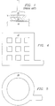
- Figures 4 and 5 depict masks utilized for patterning layers of an integrated circuit substrate to be utilized for a bond pad.
- mask 32 is utilized to form a conductive region 30 in the shape of a grid in first conductive layer 24 .
- Second conductive layer 26 is deposited over conductive region 30 and directly contacts underlying region 20 around the sides of conductive region 30 and also through the holes in the grid.
- a grid pattern allows enough of first conductive layer 24 to remain after the etching process so that first conductive layer 24 may be probe tested in a normal manner before the deposition of second conductive layer 26 and provides surface interconnect for electrical contact between first conductive layer 24 and second conductive layer 26 .
- mask 34 is utilized to form a conductive region 30 in the shape of a ring.
- a larger area of second conductive layer 26 will directly contact underlying region 20 thus further improving the adhesiveness among the layers.
- the area of first conductive layer 24 has decreased making probing more difficult.
- Other shapes, such as rectangles, may be used as a mask to pattern first conductive layer 24 .
- the method described above, and the structure formed thereby provides for an improved bonding pad by improving the adhesiveness among underlying layers of an integrated circuit device.
- an improved bond pad is formed.
- a third conductive layer may be deposited over the device while maintaining the improved adhesion between the layers.
- the present invention may provide a method, wherein the first insulating layer is comprised of oxide.
- the present invention may provide a method, wherein the barrier layer is comprised of titanium nitride.
- the present invention may provide a method, wherein the first conductive layer is comprised of polycrystaline silicon.
- the present invention may provide a method, wherein the first conductive layer is comprised of metal.
- the metal may be aluminum.
- the present invention may provide a method, wherein the second insulating layer is comprised of oxide.
- the present invention may provide a bond pad structure, wherein the sidewall regions are comprised of oxide.
- the present invention may provide a bond pad structure wherein the barrier region is comprised of titanium nitride.
- the present invention may provide a bond pad structure, wherein the conductive region is comprised of metal.
- the metal may be aluminum.
Abstract
Description
- The present invention relates generally to semiconductor integrated circuits, and more specifically to formation of a bond pad structure for such circuits.
- After an integrated circuit device has completed the fabrication process, it is usually assembled into a package to be utilized on a printed circuit board as part of a larger circuit. In order for the inner leads of the package to make electrical contact with the bonding pads of the fabricated device, a metal bond is formed at the bonding pad of the device with a lead extending to the inner lead of the package lead frame.
- During the formation of a bond, bond pad lift off may occur. This problem results when the large, heavy bond is placed on top of layers which have not formed a strong adhesion to the underlying layers. During formation of aluminum interconnect, it is common to form an underlying barrier layer of a material such as titanium nitride. This barrier layer is utilized to prevent the aluminum from spiking into any underlying conductive layers during later fabrication steps. However, the barrier layer, which is usually titanium nitride, does not form a strong adhesion to the oxide underlying the bond pad, and may separate during the bonding process.
- Therefore, it would be desirable to provide a method for forming an improved bond pad structure whereby a bond may be formed at a bonding pad which is resistant to layer separation at the bond pad.
- A method is disclosed for forming an improved bonding pad structure. A bond pad structure is formed by depositing a barrier layer over an underlying region of a semiconductor device, and then depositing a first conductive layer over the barrier layer. The barrier layer and conductive layer are then patterned and etched to define a conductive region. In a preferred embodiment, the conductive region is formed in the shape of a grid. A second conductive layer is deposited over the conductive region and a portion of the exposed underlying region. The second conductive layer makes a good adhesive contact with the underlying region, thus preventing bond pad lift off.
- The novel features believed characteristic of the invention are set forth in the appended claims. The invention itself however, as well as a preferred mode of use, and further objects and advantages thereof, will best be understood by reference to the following detailed description of an illustrative embodiment when read in conjunction with the accompanying drawings, wherein:
- Figure 1 is a sectional view of an integrated circuit illustrating a wire lead bonded to an integrated circuit substrate according to the prior art;
- Figure 2 is a sectional view of an integrated circuit taken along the line A--A in Figure 3, illustrating a wire lead bonded to an integrated circuit substrate according to the present invention;
- Figure 3 is a sectional view of an integrated circuit taken along the line B--B in Figure 2, illustrating a wire lead bonded to an integrated circuit substrate according to the present invention; and
- Figures 4 and 5 are top views of masks utilized for patterning layers of an integrated circuit substrate.
- The process steps and structures described below do not form a complete process flow for manufacturing integrated circuits. The present invention can be practiced in conjunction with integrated circuit fabrication techniques currently used in the art, and only so much of the commonly practiced process steps are included as are necessary for an understanding of the present invention. The figures representing cross-sections of portions of an integrated circuit during fabrication are not drawn to scale, but instead are drawn so as to illustrate the important features of the invention.
- Figure 1 depicts a prior art method for forming a bond in an integrated circuit. Referring to Figure 1, a bond is formed over an
underlying region 10 in an integrated circuit. Underlyingregion 10 may be either a semiconductor substrate or an underlying insulating layer. Underlyingregion 10 is typically field oxide in the peripheral region of the integrated circuit. Abarrier layer 12 is deposited over the device, followed by a firstconductive layer 14. A secondconductive layer 16 may later be deposited over firstconductive layer 14. Abond 18 is then formed from secondconductive layer 16 to a lead in the package used to house the integrated circuit device. - In one prior art embodiment,
underlying region 10 may be oxide,barrier layer 12 may be titanium nitride, and firstconductive layer 14 and secondconductive layer 16 may be aluminum. Those skilled in the art will appreciate that formingbond 18 may cause thetitanium nitride layer 12 to separate from theoxide layer 10. - Figures 2 and 3 depict a preferred method for forming an improved bond pad in an integrated circuit. Referring to Figure 2, a bond pad will be formed over an
underlying region 20 in an integrated circuit. Underlyingregion 20 may be either a semiconductor substrate or an underlying insulating layer. Abarrier layer 22, such as titanium nitride is deposited over the device, followed by a firstconductive layer 24, typically of aluminum. These are the conductive and barrier layers deposited during the typical fabrication process to form a first metal interconnect layer. As known in the art,barrier layer 22 does not adhere well to underlyinglayer 20, which causes bond pad lift off problems in the prior art method as described above. - A first insulating layer (not shown) is then deposited over first
conductive layer 24, as is typically performed during processing to form an interlevel dielectric layer. The device is then patterned and etched to remove a portion of the first insulating layer, leaving onlyresidual sidewalls 28. This step is typically performed during formation of a via between two conductive layers elsewhere in the device. The patterning and etching steps form aconductive region 30 which is comprised ofbarrier layer 22, firstconductive layer 24 andresidual sidewalls 28. Those skilled in the art will appreciate that a conductive lead typically extends from firstconductive region 30 to be utilized for connection to other parts of the chip. A secondconductive layer 26 is then deposited overconductive region 30 and exposed portions ofunderlying region 20 to define a bond pad. A bond will be made to secondconductive layer 26. In one embodiment, firstconductive layer 24 may be aluminum,barrier layer 22 may be titanium nitride,residual sidewalls 28 may be oxide, andunderlying region 20 may be oxide. Secondconductive layer 26 may be comprised of a layer of aluminum, a layer of titanium and a layer of aluminum, a layer of titanium and a layer of aluminum and a layer of titanium nitride, a layer of tungsten, or a layer of titanium and tungsten composite. Alternatively,underlying region 20 may be polycrystalline silicon. - Referring now to Figure 3, there is depicted a top view of a bond pad in accordance with the present invention. In a preferred embodiment, first
conductive layer 24 is patterned and etched to formconductive region 30 in the shape of a grid. Secondconductive layer 26 is then deposited overconductive region 30 to form a bond pad. Secondconductive layer 26 directly contacts underlyingregion 20 through the holes in the grid. In this manner, secondconductive layer 26 contacts the oxide ofunderlying region 20 which provides a good adhesive surface. Secondconductive layer 26 is now well attached so that lift off will not occur during bonding. - Figures 4 and 5 depict masks utilized for patterning layers of an integrated circuit substrate to be utilized for a bond pad. Referring to Figure 4, in a preferred embodiment of the present invention,
mask 32 is utilized to form aconductive region 30 in the shape of a grid in firstconductive layer 24. Secondconductive layer 26 is deposited overconductive region 30 and directly contacts underlyingregion 20 around the sides ofconductive region 30 and also through the holes in the grid. A grid pattern allows enough of firstconductive layer 24 to remain after the etching process so that firstconductive layer 24 may be probe tested in a normal manner before the deposition of secondconductive layer 26 and provides surface interconnect for electrical contact between firstconductive layer 24 and secondconductive layer 26. - Referring now to Figure 5, in one embodiment of the present invention,
mask 34 is utilized to form aconductive region 30 in the shape of a ring. In this embodiment, a larger area of secondconductive layer 26 will directly contact underlyingregion 20 thus further improving the adhesiveness among the layers. However, the area of firstconductive layer 24 has decreased making probing more difficult. Other shapes, such as rectangles, may be used as a mask to pattern firstconductive layer 24. - As will be appreciated by those skilled in the art, the method described above, and the structure formed thereby, provides for an improved bonding pad by improving the adhesiveness among underlying layers of an integrated circuit device. By patterning and etching a first
conductive layer 24 to expose a portion of the underlying oxide layer and then depositing a secondconductive layer 26 over conductive regions formed from the firstconductive layer 24, an improved bond pad is formed. - In an alternate embodiment, a third conductive layer may be deposited over the device while maintaining the improved adhesion between the layers.
- While the invention has been particularly shown and described with reference to a preferred embodiment, it will be understood by those skilled in the art that various changes in form and detail may be made therein without departing from the spirit and scope of the invention.
- The present invention may provide a method, wherein the first insulating layer is comprised of oxide.
- The present invention may provide a method, wherein the barrier layer is comprised of titanium nitride.
- The present invention may provide a method, wherein the first conductive layer is comprised of polycrystaline silicon.
- The present invention may provide a method, wherein the first conductive layer is comprised of metal.
- The metal may be aluminum.
- The present invention may provide a method, wherein the second insulating layer is comprised of oxide.
- The present invention may provide a bond pad structure, wherein the sidewall regions are comprised of oxide.
- The present invention may provide a bond pad structure wherein the barrier region is comprised of titanium nitride.
- The present invention may provide a bond pad structure, wherein the conductive region is comprised of metal.
- The metal may be aluminum.
Claims (13)
- A method for forming a bonding pad for an integrated circuit, comprising the steps of:
depositing a barrier layer over an underlying region of a semiconductor device;
depositing a first conductive layer over the barrier layer;
patterning and etching the first conductive layer and the barrier layer to define at least one conductive region, wherein a portion of the underlying region is exposed; and
depositing a second conductive layer over the first conductive layer, wherein the second conductive layer defines a bond pad and contacts the at least one conductive region and the exposed underlying region. - The method according to Claim 1, further comprising, after the step of patterning and etching the first conductive layer:
depositing a first insulating layer over of the at least one conductive region; and
performing an etch through the first insulating layer to form residual sidewalls along vertical sides of each conductive region. - The method according to Claim 2, wherein the step of performing an etch exposes an upper surface of the at least one conductive region and part of the exposed portion of the underlying region.
- The method according to Claim 1, wherein the step of patterning and etching the first conductive layer and the barrier layer further comprises the step of patterning and etching such layers so that the conductive region forms the shape of a grid.
- The method according to Claim 1, wherein the step of patterning and etching the first conductive layer and the barrier layer further comprises the step of patterning and etching such layers so that the conductive region forms the shape of a polygon.
- The method according to Claim 1, wherein the step of patterning and etching the first conductive layer and the barrier layer further comprises the step of patterning and etching such layers so that the conductive region forms the shape of a ring.
- The method according to Claim 1, wherein the underlying region comprises a second insulating layer.
- A bond pad structure in an integrated circuit, comprising:
a semiconductor device having an underlying region;
a conductive region deposited over the semiconductor device; and
at least one barrier region, wherein a portion of the conductive region is in direct contact with the underlying region and further wherein the remaining conductive region is separated from the underlying region by the barrier region. - The bond pad structure according to Claim 8, wherein the underlying region is oxide.
- The bond pad structure according to Claim 8, further comprising insulating sidewall regions surrounding the remaining conductive region separated from the underlying region by the barrier region.
- The bond pad structure according to Claim 8, wherein the remaining conductive region separated from the underlying region by the barrier region forms the shape of a grid.
- The bond pad structure according to Claim 8, wherein the remaining conductive region separated from the underlying region by the barrier region forms the shape of a polygon.
- The bond pad structure according to Claim 8 wherein the remaining conductive region separated from the underlying region by the barrier region forms the shape of a ring.
Applications Claiming Priority (2)
| Application Number | Priority Date | Filing Date | Title |
|---|---|---|---|
| US07/919,949 US5309025A (en) | 1992-07-27 | 1992-07-27 | Semiconductor bond pad structure and method |
| US919949 | 1992-07-27 |
Publications (2)
| Publication Number | Publication Date |
|---|---|
| EP0583877A1 true EP0583877A1 (en) | 1994-02-23 |
| EP0583877B1 EP0583877B1 (en) | 1997-11-19 |
Family
ID=25442921
Family Applications (1)
| Application Number | Title | Priority Date | Filing Date |
|---|---|---|---|
| EP93305371A Expired - Lifetime EP0583877B1 (en) | 1992-07-27 | 1993-07-08 | Bond pad structure of an integrated circuit and manufacturing method thereof |
Country Status (4)
| Country | Link |
|---|---|
| US (2) | US5309025A (en) |
| EP (1) | EP0583877B1 (en) |
| JP (1) | JP3453170B2 (en) |
| DE (1) | DE69315278T2 (en) |
Families Citing this family (22)
| Publication number | Priority date | Publication date | Assignee | Title |
|---|---|---|---|---|
| JPH0730012A (en) * | 1993-07-09 | 1995-01-31 | Fujitsu Ltd | Semiconductor device |
| US5723822A (en) * | 1995-03-24 | 1998-03-03 | Integrated Device Technology, Inc. | Structure for fabricating a bonding pad having improved adhesion to an underlying structure |
| US5703408A (en) * | 1995-04-10 | 1997-12-30 | United Microelectronics Corporation | Bonding pad structure and method thereof |
| US5707894A (en) * | 1995-10-27 | 1998-01-13 | United Microelectronics Corporation | Bonding pad structure and method thereof |
| US6049135A (en) * | 1996-05-28 | 2000-04-11 | Kabushiki Kaisha Toshiba | Bed structure underlying electrode pad of semiconductor device and method for manufacturing same |
| US5700735A (en) * | 1996-08-22 | 1997-12-23 | Taiwan Semiconductor Manufacturing Company, Ltd. | Method of forming bond pad structure for the via plug process |
| JPH10223497A (en) * | 1997-01-31 | 1998-08-21 | Shin Etsu Handotai Co Ltd | Manufacture of laminated substrate |
| US6143396A (en) * | 1997-05-01 | 2000-11-07 | Texas Instruments Incorporated | System and method for reinforcing a bond pad |
| KR100230428B1 (en) * | 1997-06-24 | 1999-11-15 | 윤종용 | Semiconductor device comprising a multi-conductive pad and method for manufacturing the same |
| WO1999038204A1 (en) * | 1998-01-23 | 1999-07-29 | Rohm Co., Ltd. | Damascene interconnection and semiconductor device |
| US5985765A (en) * | 1998-05-11 | 1999-11-16 | Taiwan Semiconductor Manufacturing Company, Ltd. | Method for reducing bonding pad loss using a capping layer when etching bonding pad passivation openings |
| US6163074A (en) | 1998-06-24 | 2000-12-19 | Samsung Electronics Co., Ltd. | Integrated circuit bonding pads including intermediate closed conductive layers having spaced apart insulating islands therein |
| US6552438B2 (en) | 1998-06-24 | 2003-04-22 | Samsung Electronics Co. | Integrated circuit bonding pads including conductive layers with arrays of unaligned spaced apart insulating islands therein and methods of forming same |
| US6187680B1 (en) | 1998-10-07 | 2001-02-13 | International Business Machines Corporation | Method/structure for creating aluminum wirebound pad on copper BEOL |
| US6191023B1 (en) * | 1999-11-18 | 2001-02-20 | Taiwan Semiconductor Manufacturing Company | Method of improving copper pad adhesion |
| US6365970B1 (en) | 1999-12-10 | 2002-04-02 | Silicon Integrated Systems Corporation | Bond pad structure and its method of fabricating |
| KR100400047B1 (en) * | 2001-11-19 | 2003-09-29 | 삼성전자주식회사 | Bonding pad structure of semiconductor device and method for forming thereof |
| US6877534B1 (en) | 2002-11-06 | 2005-04-12 | Collins L. Hendrickson, Jr. | Debris collection stand |
| TWI262347B (en) * | 2004-08-02 | 2006-09-21 | Hannstar Display Corp | Electrical conducting structure and liquid crystal display device comprising the same |
| DE602004032539D1 (en) * | 2004-09-08 | 2011-06-16 | St Microelectronics Srl | Lateral MOS array and method of making same |
| US7573115B2 (en) * | 2006-11-13 | 2009-08-11 | International Business Machines Corporation | Structure and method for enhancing resistance to fracture of bonding pads |
| US8030778B2 (en) * | 2007-07-06 | 2011-10-04 | United Microelectronics Corp. | Integrated circuit structure and manufacturing method thereof |
Citations (7)
| Publication number | Priority date | Publication date | Assignee | Title |
|---|---|---|---|---|
| EP0177251A1 (en) * | 1984-09-25 | 1986-04-09 | Nec Corporation | A semiconductor device having a reliable bonding pad structure |
| EP0337064A2 (en) * | 1988-04-15 | 1989-10-18 | International Business Machines Corporation | Alloy layer and metallurgy structure for establishing electrical contact |
| US4963511A (en) * | 1987-11-30 | 1990-10-16 | Texas Instruments Incorporated | Method of reducing tungsten selectivity to a contact sidewall |
| EP0395072A2 (en) * | 1989-04-27 | 1990-10-31 | Kabushiki Kaisha Toshiba | Bonding pad used in semiconductor device |
| EP0418777A2 (en) * | 1989-09-19 | 1991-03-27 | Fujitsu Limited | Wafer scale semiconductor device |
| EP0488186A1 (en) * | 1990-11-29 | 1992-06-03 | Kabushiki Kaisha Toshiba | Shape of bonding pad of semiconductor device bonded by wire bonding method |
| EP0490506A1 (en) * | 1990-11-24 | 1992-06-17 | Nec Corporation | Semiconductor device having a bonding pad |
Family Cites Families (14)
| Publication number | Priority date | Publication date | Assignee | Title |
|---|---|---|---|---|
| JPS61144851A (en) * | 1984-12-19 | 1986-07-02 | Hitachi Ltd | Semiconductor device |
| US4705606A (en) * | 1985-01-31 | 1987-11-10 | Gould Inc. | Thin-film electrical connections for integrated circuits |
| JPS61225837A (en) * | 1985-03-29 | 1986-10-07 | Fujitsu Ltd | Layer connection of semiconductor device |
| JPS62174934A (en) * | 1986-01-28 | 1987-07-31 | Mitsubishi Electric Corp | Semiconductor device and manufacture thereof |
| JPS6310542A (en) * | 1986-07-01 | 1988-01-18 | Nec Corp | Semiconductor device |
| JPS63283040A (en) * | 1987-05-15 | 1988-11-18 | Toshiba Corp | Semiconductor device |
| JPH01308036A (en) * | 1988-06-07 | 1989-12-12 | Toshiba Corp | Bonding pad and manufacture thereof |
| JPH02132836A (en) * | 1988-11-14 | 1990-05-22 | Seiko Epson Corp | Semiconductor device |
| JPH03235381A (en) * | 1990-02-13 | 1991-10-21 | Fujitsu Ltd | Manufacture of semiconductor device |
| US5189506A (en) * | 1990-06-29 | 1993-02-23 | International Business Machines Corporation | Triple self-aligned metallurgy for semiconductor devices |
| US5149671A (en) * | 1990-12-03 | 1992-09-22 | Grumman Aerospace Corporation | Method for forming multilayer indium bump contact |
| JPH04288843A (en) * | 1991-03-07 | 1992-10-13 | Mitsubishi Electric Corp | Semiconductor device |
| US5316976A (en) * | 1992-07-08 | 1994-05-31 | National Semiconductor Corporation | Crater prevention technique for semiconductor processing |
| US5248903A (en) * | 1992-09-18 | 1993-09-28 | Lsi Logic Corporation | Composite bond pads for semiconductor devices |
-
1992
- 1992-07-27 US US07/919,949 patent/US5309025A/en not_active Expired - Lifetime
-
1993
- 1993-07-08 DE DE69315278T patent/DE69315278T2/en not_active Expired - Fee Related
- 1993-07-08 EP EP93305371A patent/EP0583877B1/en not_active Expired - Lifetime
- 1993-07-27 JP JP18522393A patent/JP3453170B2/en not_active Expired - Fee Related
-
1994
- 1994-01-14 US US08/182,845 patent/US5403777A/en not_active Expired - Lifetime
Patent Citations (7)
| Publication number | Priority date | Publication date | Assignee | Title |
|---|---|---|---|---|
| EP0177251A1 (en) * | 1984-09-25 | 1986-04-09 | Nec Corporation | A semiconductor device having a reliable bonding pad structure |
| US4963511A (en) * | 1987-11-30 | 1990-10-16 | Texas Instruments Incorporated | Method of reducing tungsten selectivity to a contact sidewall |
| EP0337064A2 (en) * | 1988-04-15 | 1989-10-18 | International Business Machines Corporation | Alloy layer and metallurgy structure for establishing electrical contact |
| EP0395072A2 (en) * | 1989-04-27 | 1990-10-31 | Kabushiki Kaisha Toshiba | Bonding pad used in semiconductor device |
| EP0418777A2 (en) * | 1989-09-19 | 1991-03-27 | Fujitsu Limited | Wafer scale semiconductor device |
| EP0490506A1 (en) * | 1990-11-24 | 1992-06-17 | Nec Corporation | Semiconductor device having a bonding pad |
| EP0488186A1 (en) * | 1990-11-29 | 1992-06-03 | Kabushiki Kaisha Toshiba | Shape of bonding pad of semiconductor device bonded by wire bonding method |
Also Published As
| Publication number | Publication date |
|---|---|
| JP3453170B2 (en) | 2003-10-06 |
| EP0583877B1 (en) | 1997-11-19 |
| DE69315278T2 (en) | 1998-04-02 |
| US5403777A (en) | 1995-04-04 |
| US5309025A (en) | 1994-05-03 |
| JPH06204281A (en) | 1994-07-22 |
| DE69315278D1 (en) | 1998-01-02 |
Similar Documents
| Publication | Publication Date | Title |
|---|---|---|
| EP0583877B1 (en) | Bond pad structure of an integrated circuit and manufacturing method thereof | |
| US5834365A (en) | Method of forming a bonding pad | |
| US5707894A (en) | Bonding pad structure and method thereof | |
| US5470793A (en) | Method of via formation for the multilevel interconnect integrated circuits | |
| US6444295B1 (en) | Method for improving integrated circuits bonding firmness | |
| US5723822A (en) | Structure for fabricating a bonding pad having improved adhesion to an underlying structure | |
| US20020005568A1 (en) | Semiconductor device and method for manufacturing | |
| US6306750B1 (en) | Bonding pad structure to prevent inter-metal dielectric cracking and to improve bondability | |
| US20020084513A1 (en) | Integrated circuits and methods for their fabrication | |
| EP1609179B1 (en) | Internally reinforced bond pads | |
| EP0540312B1 (en) | Bump electrode structure and semiconductor chip having the same | |
| US6084312A (en) | Semiconductor devices having double pad structure | |
| KR100691051B1 (en) | Dual damascene bond pad structure for lowering stress and allowing circuitry under pads and a process to form the same | |
| EP0899788A2 (en) | Semiconductor device and method with improved flat surface | |
| EP0547906B1 (en) | Method for forming contact vias in integrated circuits | |
| EP1003209A1 (en) | Process for manufacturing semiconductor device | |
| US5915201A (en) | Trench surrounded metal pattern | |
| EP0056908A2 (en) | Semiconductor device | |
| CA2634599C (en) | Thinned image sensor with trench-insulated contact terminals | |
| EP0415526A2 (en) | Semiconductor device having wiring layers | |
| JPH03268385A (en) | Solder bump and manufacture thereof | |
| JPS62136857A (en) | Manufacture of semiconductor device | |
| JP2822879B2 (en) | Semiconductor device manufacturing method and etching method | |
| JP2739842B2 (en) | Method for manufacturing semiconductor device | |
| KR100313530B1 (en) | Pad forming method for semiconductor device |
Legal Events
| Date | Code | Title | Description |
|---|---|---|---|
| PUAI | Public reference made under article 153(3) epc to a published international application that has entered the european phase |
Free format text: ORIGINAL CODE: 0009012 |
|
| AK | Designated contracting states |
Kind code of ref document: A1 Designated state(s): DE FR GB IT |
|
| 17P | Request for examination filed |
Effective date: 19940818 |
|
| 17Q | First examination report despatched |
Effective date: 19960425 |
|
| GRAG | Despatch of communication of intention to grant |
Free format text: ORIGINAL CODE: EPIDOS AGRA |
|
| GRAH | Despatch of communication of intention to grant a patent |
Free format text: ORIGINAL CODE: EPIDOS IGRA |
|
| GRAH | Despatch of communication of intention to grant a patent |
Free format text: ORIGINAL CODE: EPIDOS IGRA |
|
| GRAA | (expected) grant |
Free format text: ORIGINAL CODE: 0009210 |
|
| AK | Designated contracting states |
Kind code of ref document: B1 Designated state(s): DE FR GB IT |
|
| REF | Corresponds to: |
Ref document number: 69315278 Country of ref document: DE Date of ref document: 19980102 |
|
| ITF | It: translation for a ep patent filed |
Owner name: PORTA CHECCACCI E BOTTI S.R.L. |
|
| ET | Fr: translation filed | ||
| PGFP | Annual fee paid to national office [announced via postgrant information from national office to epo] |
Ref country code: GB Payment date: 19980629 Year of fee payment: 6 |
|
| PGFP | Annual fee paid to national office [announced via postgrant information from national office to epo] |
Ref country code: FR Payment date: 19980709 Year of fee payment: 6 |
|
| PGFP | Annual fee paid to national office [announced via postgrant information from national office to epo] |
Ref country code: DE Payment date: 19980720 Year of fee payment: 6 |
|
| PLBE | No opposition filed within time limit |
Free format text: ORIGINAL CODE: 0009261 |
|
| STAA | Information on the status of an ep patent application or granted ep patent |
Free format text: STATUS: NO OPPOSITION FILED WITHIN TIME LIMIT |
|
| 26N | No opposition filed | ||
| PG25 | Lapsed in a contracting state [announced via postgrant information from national office to epo] |
Ref country code: GB Free format text: LAPSE BECAUSE OF NON-PAYMENT OF DUE FEES Effective date: 19990708 |
|
| PG25 | Lapsed in a contracting state [announced via postgrant information from national office to epo] |
Ref country code: FR Free format text: THE PATENT HAS BEEN ANNULLED BY A DECISION OF A NATIONAL AUTHORITY Effective date: 19990731 |
|
| GBPC | Gb: european patent ceased through non-payment of renewal fee |
Effective date: 19990708 |
|
| PG25 | Lapsed in a contracting state [announced via postgrant information from national office to epo] |
Ref country code: DE Free format text: LAPSE BECAUSE OF NON-PAYMENT OF DUE FEES Effective date: 20000503 |
|
| REG | Reference to a national code |
Ref country code: FR Ref legal event code: ST |
|
| PG25 | Lapsed in a contracting state [announced via postgrant information from national office to epo] |
Ref country code: IT Free format text: LAPSE BECAUSE OF NON-PAYMENT OF DUE FEES;WARNING: LAPSES OF ITALIAN PATENTS WITH EFFECTIVE DATE BEFORE 2007 MAY HAVE OCCURRED AT ANY TIME BEFORE 2007. THE CORRECT EFFECTIVE DATE MAY BE DIFFERENT FROM THE ONE RECORDED. Effective date: 20050708 |