EP0580294B1 - Automatic frequency control circuit - Google Patents
Automatic frequency control circuit Download PDFInfo
- Publication number
- EP0580294B1 EP0580294B1 EP93304891A EP93304891A EP0580294B1 EP 0580294 B1 EP0580294 B1 EP 0580294B1 EP 93304891 A EP93304891 A EP 93304891A EP 93304891 A EP93304891 A EP 93304891A EP 0580294 B1 EP0580294 B1 EP 0580294B1
- Authority
- EP
- European Patent Office
- Prior art keywords
- frequency
- signal
- receiver
- count
- value
- Prior art date
- Legal status (The legal status is an assumption and is not a legal conclusion. Google has not performed a legal analysis and makes no representation as to the accuracy of the status listed.)
- Expired - Lifetime
Links
- 230000010355 oscillation Effects 0.000 claims description 58
- 238000000034 method Methods 0.000 claims description 43
- 230000008569 process Effects 0.000 claims description 31
- 230000001629 suppression Effects 0.000 claims description 28
- 230000005684 electric field Effects 0.000 claims description 25
- 230000004044 response Effects 0.000 claims description 16
- 238000004904 shortening Methods 0.000 claims description 3
- 238000005562 fading Methods 0.000 description 26
- 230000005540 biological transmission Effects 0.000 description 14
- 238000012937 correction Methods 0.000 description 8
- 230000006870 function Effects 0.000 description 6
- 239000000470 constituent Substances 0.000 description 5
- 238000012545 processing Methods 0.000 description 5
- 230000010267 cellular communication Effects 0.000 description 4
- 230000000694 effects Effects 0.000 description 4
- 230000014509 gene expression Effects 0.000 description 4
- 230000000087 stabilizing effect Effects 0.000 description 4
- 230000006641 stabilisation Effects 0.000 description 3
- 238000011105 stabilization Methods 0.000 description 3
- 238000006243 chemical reaction Methods 0.000 description 2
- 230000003247 decreasing effect Effects 0.000 description 2
- 238000010586 diagram Methods 0.000 description 2
- 238000011156 evaluation Methods 0.000 description 2
- 230000007257 malfunction Effects 0.000 description 2
- 230000002035 prolonged effect Effects 0.000 description 2
- 230000002411 adverse Effects 0.000 description 1
- 230000008901 benefit Effects 0.000 description 1
- 230000008859 change Effects 0.000 description 1
- 238000004891 communication Methods 0.000 description 1
- 239000013078 crystal Substances 0.000 description 1
- 239000000284 extract Substances 0.000 description 1
- 230000007274 generation of a signal involved in cell-cell signaling Effects 0.000 description 1
- 230000010363 phase shift Effects 0.000 description 1
- 230000000630 rising effect Effects 0.000 description 1
- 238000007493 shaping process Methods 0.000 description 1
Images


Classifications
-
- H—ELECTRICITY
- H03—ELECTRONIC CIRCUITRY
- H03D—DEMODULATION OR TRANSFERENCE OF MODULATION FROM ONE CARRIER TO ANOTHER
- H03D7/00—Transference of modulation from one carrier to another, e.g. frequency-changing
- H03D7/16—Multiple-frequency-changing
-
- H—ELECTRICITY
- H03—ELECTRONIC CIRCUITRY
- H03J—TUNING RESONANT CIRCUITS; SELECTING RESONANT CIRCUITS
- H03J7/00—Automatic frequency control; Automatic scanning over a band of frequencies
- H03J7/02—Automatic frequency control
- H03J7/026—Means preventing a wrong working of the automatic frequency correction in case of fading or bad signal/noise ratio
-
- H—ELECTRICITY
- H03—ELECTRONIC CIRCUITRY
- H03J—TUNING RESONANT CIRCUITS; SELECTING RESONANT CIRCUITS
- H03J7/00—Automatic frequency control; Automatic scanning over a band of frequencies
- H03J7/02—Automatic frequency control
- H03J7/04—Automatic frequency control where the frequency control is accomplished by varying the electrical characteristics of a non-mechanically adjustable element or where the nature of the frequency controlling element is not significant
- H03J7/06—Automatic frequency control where the frequency control is accomplished by varying the electrical characteristics of a non-mechanically adjustable element or where the nature of the frequency controlling element is not significant using counters or frequency dividers
- H03J7/065—Automatic frequency control where the frequency control is accomplished by varying the electrical characteristics of a non-mechanically adjustable element or where the nature of the frequency controlling element is not significant using counters or frequency dividers the counter or frequency divider being used in a phase locked loop
Definitions
- This invention relates to an automatic frequency control (AFC) circuit used at a mobile station for digital communication and more particularly to an AFC circuit which causes the oscillation frequency of an oscillator contained in the mobile station to follow the frequency of a signal received from a base station and stabilizes it.
- AFC automatic frequency control
- Another automatic frequency control circuit is described in EP-A-0,339,647.
- the described circuit mixes a second IF signal with an oscillation signal outputted from an oscillator.
- a third IF signal is obtained having a frequency lower than the frequency of the second IF signal.
- a counter circuit counts the third IF signal.
- the frequency of the second IF signal is then adjusted on the basis of the counting of the counter circuit.
- a receiver of a mobile station adopts a superheterodyne system which requires a local oscillator to convert a reception frequency into an intermediate frequency.
- the configuration can be used which includes a high-precision reference oscillator which oscillates at a high frequency and a circuit which converts an oscillation output of the reference oscillator into a predetermined local oscillation frequency.
- a voltage-controlled and temperature-compensated crystal oscillator VC-TCXO
- a circuit such as a multiplying circuit, or a phase locked loop (PLL) synthesizer can be used.
- the intermediate frequency signal provided by making frequency conversion of a signal received from the base station shifts from the predetermined frequency. If the frequency of the intermediate frequency signal shifts from the predetermined value, the received data cannot accurately be demodulated and the transmission frequency from the mobile station becomes incorrect.
- an AFC circuit is used at the mobile station to remove or correct the deviation of the local oscillation frequency.
- the receiver has first intermediate frequency F IF1 and second intermediate frequency F IF2 as intermediate frequencies.
- the control object value of the oscillation frequency of the reference oscillator i.e. the reference frequency is F 0 and that the first and second local oscillation frequencies provided by performing steps such as multiplying the value are F L1 and F L2 respectively.
- the first and second intermediate frequencies provided by frequency conversion, F IF1 and F IF2 can be represented by the following expressions using the frequency of reception signal, i.e. the reception frequency F R :
- F IF1 F L1 - F R
- the reference frequency contains a deviation ⁇ , that is, if the reference oscillator oscillates at F 0 (1+ ⁇ ), the values of the first and second local oscillation frequencies become F L1 (1+ ⁇ ) and F L2 (1+ ⁇ ) respectively. As a result, the first and second intermediate frequencies also contain a deviation.
- F IF1 ' F L1 (1+ ⁇ ) - F R
- ⁇ appears only in the second term. Therefore, if the oscillation frequency of the reference oscillator is subjected to feedback control so that the count value D A becomes the value of the first term n/F 0 x F IF2 the reference frequency can be controlled to the object value F 0 . Based on such relationships, the AFC circuit controls the reference frequency. That is, n/F 0 x F IF2 - D A is multiplied by predetermined coefficient ⁇ to find value D B at step S22, and the value D B is used as correction data to control the reference frequency F 0 at step S23.
- the AFC circuit can stabilize the oscillation frequency of a reference oscillator such as a VC-TCXO.
- the frequency deviation allowed for a mobile station is a small value of ⁇ 200 Hz.
- the transmission frequency of the base station is an 800 MHz band, it is understood that the frequency deviation tolerance is a strict value of ⁇ 0.25 ppm.
- the reference frequency stablizing time at hand off is short: Within 130 msec at -90 dBm input and within 250 msec at -103 dBm input.
- the time for counting the second intermediate frequency generally containing a deviation, F IF2 ' is set to, for example, 100 msec counting on a margin for the time 130 msec, a frequency error exceeding the specification of ⁇ 200 Hz will occur due to fading or any other cause.
- the counting time needs only to be prolonged. However, if the time is prolonged, the stabilizing performance at hand off becomes insufficient.
- a modulation pattern needs to be random to suitably perform the control described above, that is, in-band constituents of reception frequencies need to be distributed equally with the center frequency as the center.
- frequency selective fading such as multipath fading or multifrequency fading occurs
- the high or low partial frequency constituent is lost with respect to the center frequency of the reception frequencies.
- the count value D A becomes a value lower than the center frequency.
- the delay time caused by multipath fading is 40 usec at maximum, thus the fading pitch becomes short (25 kHz) and the frequency deviation standard of ⁇ 200 Hz cannot be satisfied.
- a count error is caused by a temporary drop in the input level at fading. Since random noise in nature is counted in the period during which the input level drops, a count error occurs. If a reception signal in analog form is supplied to count processing, a count error (malfunction of digital circuit) may occur due to disorder cr incompletion of the waveform of the signal.
- an automatic frequency control circuit for use with a receiver which mixes a reception signal with a local oscillation signal to generate an intermediate frequency signal
- the automatic frequency control circuit comprising means for counting a frequency of the intermediate frequency signal for a predetermined time, means responsive to a count value by said counting means for controlling a frequency of the local oscillation signal, means for determining whether or not an error is prone to occur in the count value, and means responsive to a determination result by said determining means for executing an error suppression process for suppressing an error of the count value, characterised in that said determining means includes means for observing variations in said count values in a time series manner, and means for determining whether or not the variations obtained by observation exceed a predetermined deviation from a centre value, and said error suppression process execution means has means for handling said count values as invalid values and excluding them from a base of control of the local oscillation frequency if the variations do exceed said predetermined deviation.
- a method of controlling frequencies for use with a receiver which mixes a reception signal with a local oscillation signal to generate an intermediate frequency signal comprising the steps of: counting a frequency of the intermediate frequency signal for a predetermined time, controlling a frequency of the local oscillation signal in response to a count value provided by said counting step, determining whether or not an error is prone to occur in the count value, and executing an error suppression process for suppressing an error of the count value in response to a determination result provided by said determining step, characterised in that said determining step includes observing variations in said count values in a time series manner, and determining whether or not the variations obtained by observation exceed a predetermined deviation from a centre value, said error suppression step including handling said count values as invalid values and excluding them from a base of control of the local oscillation frequency if the variations do exceed said predetermined deviation.
- a frequency of an intermediate frequency signal is counted for the predetermined time, and the local oscillator signal frequency is controlled in response to the count value.
- the error suppression process is to suppress an error when it is prone to occur in the count value. Therefore, even if the electric field input level drops, fading occurs, or a modulation pattern deviation occurs, the invention is capable of reacting to them for accurate frequency control.
- the error suppression process is embodied by the following process: the variations in the count values are observed in a time series manner, and if the variations obtained by the observation are comparatively large, the count values are handled as invalid values and are excluded from the control base of the local oscillation frequency. Therefore, the missing of the high frequency constituent, caused by a modulation pattern deviation, fading, etc., can be overcome by executing the process.
- the error suppression process is realized as follows, for example: the variations in the count values are observed in a time series manner, and if the variations obtained by the observation are comparatively small, the observed count values comparatively distant from a predetermined centre value are excluded from the control base of the local oscillation frequency. Thus, only the count values near the centre value and comparatively worthy of trust can be used for frequency control.
- the error suppression process is embodied as follows: the variations in the count values are observed in a time series manner, and if the variations obtained by observation are comparatively large, the count values are handled as invalid values and are excluded from the control base of the local oscillation frequency; if comparatively small, the observed count values comparatively distant from a predetermined centre value are excluded from the control base of the local oscillation frequency.
- the missing of the high frequency constituent caused by a modulation pattern deviation, fading, etc., can be overcome, and only the count values near the centre value and comparatively worthy of trust can be used for frequency control.
- the error suppression process is embodied by the process of prolonging the count time if the electric field input level to the receiver is low.
- the electric field input level which is low can be overcome by executing the process.
- the process is embodied by the process of shortening the count time if the receiver is in the hand-off state. This process can be executed when high-speed frequency stabilization is required.
- the error suppression process is embodied by the following process; if the receiver is not in the hand-off state, the count time is set comparatively long; if the receiver is in the hand-off state, the count time is set in response to the specification of the time required to stabilize the frequency of the local oscillation signal at hand off within the control object range and in response to the detected electric field input level. This process is significant to the situation that the high-speed frequency stabilization is required and the electric field input level becomes low. By this process, both of these problems can be overcome.
- the error suppression process is embodied by the process using hysteresis comparison, square wave generation, and self-oscillation.
- the level of an intermediate frequency signal is compared with a threshold having a hysteresis characteristic for shaping the intermediate frequency signal to a square wave, and a signal indicating the timing of the obtained square wave is supplied to count processing.
- the threshold values are set so that they are crossed when the intermediate frequency signal has a sufficient amplitude. If the level of the intermediate frequency signal drops due to the effect of fading etc., a signal having a frequency substantially equal to the control object value of the intermediate frequency signal is supplied to count processing. Then, even if the level temporarily drops due to fading, random noise in nature is not counted, thus more accurate counting, in its turn, frequency control can be performed.
- the local oscillation signal generation means may be made up of a reference oscillator which oscillates at a predetermined reference frequency and a local oscillator which converts a frequency of an output signal of the reference oscillator into a lower frequency for generating a local oscillation signal.
- the number of local oscillation frequencies may conform to the number of intermediate frequencies.
- An output of the reference oscillator may also be used for generation of a transmission frequency.
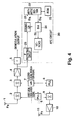
- Figure 1 shows the configuration of a mobile station according to one embodiment of the invention.
- the circuitry shown in Figure 1 comprises a receiver of a superheterodyne system, a transmitter which transmits signals to a base station, and an AFC circuit for stabilizing local oscillation frequencies at the receiver and transmitter.
- the receiver comprises a reception antenna 1, mixers 2 and 3, an amplifier 4, a code determination circuit 5, a PLL synthesizer 6, and a multiplying-by-N circuit 7.
- the reception antenna 1 is an antenna for receiving signals transmitted from the base station.
- the mixer 2 mixes a received signal with the first local oscillation signal having the first local oscillation frequency F L1 , thereby converting the received signal from the reception frequency from the base station, F R , into the first intermediate frequency F IF1 .
- the mixer 3 mixes the received signal converted into the first intermediate frequency F IF1 with the second local oscillation signal having the second local oscillation frequency F L2 , thereby converting the received signal from the first intermediate frequency F IF1 into the second intermediate frequency F IF2 .
- the amplifier 4 amplifies the signal of the second intermediate frequency F IF2 provided by the mixer 3 and sends the resultant signal to the code determination circuit 5.
- the code determination circuit 5 performs the determinition of the code transmitted from the base station based on the amplified signal, and sends the determination result to a circuit at the following stage (not shown) as demodulation output.
- the PLL synthesizer 6 makes up a first local oscillator in cooperation with a VC-TCXO 25 contained in the AFC circuit. That is, the PLL synthesizer 6 synchronizes in phase with reference frequency F 0 output from the VC-TCXO 25 for generating the first local oscillation signal having the first local oscillation frequency F L1 . Also, the multiplying-by-N circuit 7 makes up a second local oscillator in cooperation with the VC-TCXO. That is, the multiplying-by-N circuit 7 multiplies by N the period of the signal of the reference frequency F 0 output from the VC-TCXO 25, thereby generating the second local oscillation signal having the second local oscillation frequency F L2 .
- Figure 1 also shows the transmitter comprising a PLL synthesizer 8, a mixer 9, an amplifier 10, and a transmission antenna 11.
- the PLL synthesizer 8 synchronizes in phase with an output of the VC-TCXO 25 for generating an intermediate frequency signal for transmission having an intermediate frequency for transmission F IFT .
- the mixer 9 mixes the intermediate frequency signal for transmission with the first local oscillation signal, thereby generating a transmission signal having a transmission frequency F T .
- the amplifier 10 amplifies the transmission signal.
- the transmission antenna 11 is an antenna for transmitting the amplified transmission signal to the base station, etc.
- FIG. 1 further shows a received signal strength indicator (RSSI) circuit 12, an analog-to-digital (A/D) converter 13, and the AFC circuit 20.
- RSSI received signal strength indicator
- A/D analog-to-digital
- the RSSI circuit 12 monitors an output of the amplifier 4 and generates a DC voltage showing the electric field input level to the reception antenna 1, then sends the voltage to the A/D converter.
- the A/D converter converts the received DC voltage into digital data and sends the resultant digital data to an arithmetic section 22 of the AFC circuit 20.
- the arithmetic section 22 transmits the received digital data to the base station and uses it for AFC control as described below.
- the AFC circuit 20 comprises of a counter 21, the arithmetic section 22, a ROM 23, a digital-to-analog (D/A) converter, and the VC-TCXO 25.
- the counter 21 counts the frequency of the second intermediate frequency signal, namely, the second intermediate frequency generally containing a deviation, F IF2 ', for the gate time G T .
- the arithmetic section 22 reads the count result D A and performs predetermined processing described below.
- the ROM 23 is a memory which stores programs and coefficient values required for processing at the arithmetic section 22.
- the D/A converter 24 converts correction data D B output from the arithmetic section 22 into an analog signal.
- the oscillation frequency of the VC-TCXO 25 is corrected in response to the analog signal output from the D/A converter 24.
- the AFC circuit 20 applies feedback control of the oscillation frequency of the VC-TCXO 25. Since a single reference generater, namely the VC-TCXO 25 is used, the circuit configuration is simplified. Since the output of the VC-TCXO 25 is used for the generation of not only first and second local oscillation frequencies F L1 and F L2 , but also intermediate frequency for transmission F IFT , the transmission frequency F T is also made accurate by the operation of the AFC circuit.
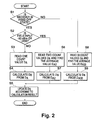
- Figure 2 shows an operation flow of the arithmetic section 22 of the mobile station according to the invention.
- the arithmetic section 22 determines whether or not the receiver is in the hand-off state at present. That is, it determines whether or not the receiver in Figure 1 moves from one radio zone (cell) to another and radio line connection is being transferred between the radio zones (cells). If the receiver is not in the hand-off state, the arithmetic section 22 executes steps S8, S9, and S5 in order.
- the average value of count values D A provided by the counter 21 is found. For example, the time average value D A30 of 30 count values D A is calculated. Assuming that it takes 100 msec to provide one count value D A , it takes 3 sec to provide 30 count values D A . Therefore, the average value D A30 is the average value for 3 sec.
- the arithmetic section 22 performs an operation of correction data D B in response to the average value D A30 .
- the operation method may be the same as the method described in Description of the Related Art.
- the correction data D B found at step S9 is output to the D/A converter 24.
- the oscillation frequency of the VC-TCXO 25 is subjected to feedback control.
- the arithmetic section 22 determines whether or not the electric field input level detected by the RSSI circuit 12 and converted into digital data by the A/D converter 13 is a predetermined value or less.
- -90 dBm should be used as the threshold value for determination in the digital cellular communication system of USA specifications, but the invention is not limited to the threshold value.
- steps S3 and S6 are input steps of count value D A ; at the former step, an average operation on the count value D A is not performed; whereas at the latter step, an average operation on two count values D A is performed.
- steps S4 and S7 are operation steps of correction data D B ; at the former step, as its base, one count value D A is used; while at the latter step, the average value D A2 found at step S6 is used.
- the total count time is selected in response to the electric field input level to meet the specification requirement for the VC-TCXO 25 stabilizing time at hand off.
- the electric field input level is -90 dBm at hand off
- the VC-TCXO 25 oscillation frequency must be stabilized within the object range within 130 msec; if it is -103 dBm, the VC-TCXO 25 oscillation frequency must be stabilized within the object range within 250 msec.
- the total count time, when the electric field input level is -90 dBm is set to 200 msec which is a value near 250 msec.
- the total count time is changed in response to the stabilization time required at hand off, thereby suppressing an error caused by a modulation pattern or fading and performing accurate reference frequency control even if the electric field input level is low, thus the S/N ratio is low.
- the reference frequency can be controlled quickly.
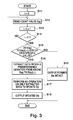
- Figure 3 shows an operation flow of an arithmetic section according to an embodiment of the invention.
- the embodiment has the same circuit configuration as the configuration in Figure 1, thus circuit parts identical with or similar to those previously described above in Figure 1 and steps identical with or similar to those previously described in Figure 2 are denoted by the same reference numerals here.
- the count time of counter 21 is set to a comparatively small value. That is, the time resulting from dividing the former gate time described in Description of the Related Art into C equal parts (C: an integer of 2 or greater) is set as the gate time of the counter 21.
- the arithmetic section 22 reads C count values of the counter 21 consecutively at steps S11 to S14, namely, reads ith count value D Ai while incrementing i by one from 0 to C-1.
- the arithmetic section 22 determines whether not the read count values D A0 to D A(C-1) center on a specific value (center value d), namely, evaluates how many pieces of the count values D A0 to D A(C-1) distribute around the center value d (concentration degree). If the concentration degree is judged to be sufficiently high as a result of the evaluation, the arithmetic section 22 extracts only data of the count values D A0 to D A(C-1) within a predetermined deviation from the center value d at step S16, uses only the extracted count values to generate correction data D B at step S17, and outputs the generated correction value D B to D/A converter 24 at step S18. If the concentration degree is judged to be low as a result of the evaluation at step 15, the arithmetic section 22 does not update correction data D B and outputs it intact to the D/A converter 24 at step 19.
- the count value containing the error is not used for reference frequency control, thereby accurately controlling the reference frequency without the effect of multipath fading, etc.
- Figure 4 shows a second configuration of a mobile station according to the invention.
- the mobile station is newly provided with an IF protecting circuit 26.
- the RSSI circuit 12 and A/D converter 13 in Figure 1 are omitted for simplicity of Figure 4.
- Circuit parts identical with or similar to those previously described with reference to Figure 1 are denoted by the same reference numerals in Figure 4 and will therefore not be discussed again.
- the IF protecting circuit has a comparison function having a hysteresis characteristic and a self-oscillating function at a predetermined second intermediate frequency F IF2 .
- Figure 4 does not show the internal configuration of the IF protecting circuit 26, those skilled in the art would be able to configure the IF protecting circuit by using parts such as a hysteresis comparator, a pulse generator, and a logic circuit, based on the description that follows.
- the IF protecting circuit 26 is a circuit provided to enable the reference frequency F 0 to be controlled accurately even if fading where the reception signal level temporarily drops occurs.
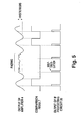
- Figure 5 shows the function and operation of the IF protecting circuit 26.
- the IF protecting circuit 26 compares an output of amplifier 4 with a predetermined threshold value.
- the comparison function of the IF protecting circuit 26 has a hysteresis characteristic. Therefore, the threshold value with which the output of the amplifier 4 is to be compared in the period during which the output of the amplifier 4 is increasing differs from that in the period during which the output is decreasing.
- the threshold value in the period during which the output of the amplifier 4 is increasing is comparatively high; that in the period during which the output is decreasing is comparatively low, as shown in Figure 5.
- the IF protecting circuit 26 While executing the comparison, the IF protecting circuit 26 self-oscillates a pulse at a frequency substantially equal to the second intermediate frequency F IF2 , and then outputs the oscillated pulse to counter 21 in synchronization with the rising edge of a square wave signal resulting from the comparison.
- the counter 21 counts pulses output from the IF protecting circuit 26, thereby detecting the second intermediate frequency F IF2 suitably.
- the output amplitude of the amplifier 4 may temporarily drop as shown in Figure 5.
- the output of the amplifier 4 does not cross threshold values, thus no square wave signal is obtained even if a hysteresis comparison is made.
- the IF protecting circuit outputs self-oscillated pulses to the counter 21.
- the self-oscillation frequency is substantially equal to the second intermediate frequency F IF2 . Therefore, even if the output amplitude of the amplifier 4 temporarily drops due to the effect of fading, randomness of the fading waveform (randomness of natural noise) does not adversely affect the count result of the counter 21.
- the IF protecting circuit 26 detects occurrence of a temporary drop in the output amplitude of the amplifier 4 when the elapsed time since the instance of the previous change of the result value of hysteresis comparison exceeds the predetermined time.
- Those skilled in the art will be able to implement the function by using a timer, etc.
- the self-oscillation output function of the IF protecting circuit 26 provides an advantage of being able to control the VC-TCXO 25 oscillation frequency more accurately as a result. Since the hardware configuration of the IF protecting circuit 26 may be very simple, the configuration and scale of the mobile station may be comparatively simple and small. Further, the IF protecting circuit 26 shapes an output of the amplifier 4 to a square wave. This means that a waveform appropriate for the following digital circuitry containing the counter 21 is provided by the IF protecting circuit 26. This suppresses a malfunction of the digital circuitry.
Landscapes
- Engineering & Computer Science (AREA)
- Power Engineering (AREA)
- Channel Selection Circuits, Automatic Tuning Circuits (AREA)
- Superheterodyne Receivers (AREA)
- Circuits Of Receivers In General (AREA)
Description
Claims (12)
- An automatic frequency control circuit (20) for use with a receiver which mixes a reception signal (FIF1) with a local oscillation signal (FL2) to generate an intermediate frequency signal (FIF2), the automatic frequency control circuit (20) comprising means (21) for counting a frequency of the intermediate frequency signal (FIF2) for a predetermined time (GT); means (22) responsive to a count value (DA) by said counting means (21) for controlling a frequency of the local oscillation signal (FL2); means for determining whether or not an error is prone to occur in the count value (DA); and means responsive to a determination result by said determining means for executing an error suppression process for suppressing an error of the count value, characterised in that said determining means includes means for observing variations in said count values (DA) in a time series manner; and means for determining whether or not the variations obtained by observation exceed a predetermined deviation from a centre value (d); and said error suppression process execution means has means for handling said count values (DA) as invalid values and excluding them from a base of control (DB) of the local oscillation frequency (FL2) if the variations do exceed said predetermined deviation.
- The automatic frequency control circuit as claimed in claim 1, wherein said error suppression process execution means has means for excluding from a base of control (DB) of the local oscillation frequency (FL2) those observed count values (DA) which fall within said predetermined deviation but which deviate from said predetermined centre value (d) to a greater extent.
- The automatic frequency control circuit as claimed in claim 1, wherein said determining means additionally comprises means (12) for detecting an electric field input level to the receiver; and said error suppression process execution means has means for prolonging said count time (GT) if the detected electric field input level is less than a predetermined value.
- The automatic frequency control circuit as claimed in claim 1, wherein said determining means additionally comprises means for detecting whether the receiver is in a hand-off state; and said error suppression process execution means has means for shortening said count time (GT) if the receiver is in said hand-off state.
- The automatic frequency control circuit as claimed in claim 1, wherein said determining means additionally comprises means for detecting whether the receiver is in a hand-off state; and said error suppression process execution means has means for setting said count time (GT) to a predetermined value if the receiver is not in said hand-off state; said determining means further including means (12) for detecting an electric field input level to the receiver if the receiver is in said hand-off state; and said error suppression process execution means further including means for setting said count time (GT) in response to a specification of time required to stabilize the frequency of the local oscillation signal (FL2) at hand off within a control object range and in response to the detected electric field input level.
- The automatic frequency control circuit as claimed in claim 1, wherein said determining means additionally comprises means (26) for comparing a level of the intermediate frequency signal (FIF2) with threshold values having a hysteresis characteristic for generating a square wave; said threshold values being set so as to be crossed if the intermediate frequency signal (FIF2) has a sufficient amplitude; and said error suppression process execution means includes means for supplying a signal indicating a timing of the square wave signal to said counting means (21) as an object of counting when a square wave signal is generated as a result of the comparison; and means for supplying a signal having a frequency substantially equal to a control target value of the intermediate frequency signal (FIF2) to said counting means (21) as an object of counting when a square wave signal is not generated as a result of the comparison.
- A method of controlling frequencies for use with a receiver which mixes a reception signal (FIF1) with a local oscillation signal (FL2) to generate an intermediate frequency signal (FIF2), the method comprising the steps of: counting a frequency of the intermediate frequency signal (FIF2) for a predetermined time (GT); controlling a frequency of the local oscillation signal (FL2) in response to a count value (DA) provided by said counting step; determining whether or not an error is prone to occur in the count value (DA); and executing an error suppression process for suppressing an error of the count value (DA) in response to a determination result provided by said determining step, characterised in that said determining step includes observing variations in said count values (DA) in a time series manner; and determining whether or not the variations obtained by observation exceed a predetermined deviation from a centre value (d), said error suppression step including handling said count values (DA) as invalid values and excluding them from a base of control (DB) of the local oscillation frequency (FL2) if the variations do exceed said predetermined deviation.
- The method as claimed in claim 7, wherein said error suppression step including excluding from a base of control (DB) of the local oscillation frequency (FL2) those observed count values (DA) which fall within said predetermined deviation but which deviate from said predetermined centre value (d) to a greater extent.
- The method as claimed in claim 7, wherein said determining step further includes detecting an electric field input level to the receiver; and said error suppression step includes prolonging said count time (GT) if the detected electric field input level is less than a predetermined value.
- The method as claimed in claim 7, wherein said determining step further includes detecting whether the receiver is in a hand-off state; and said error suppression step includes shortening said count time (GT) if the receiver is in said hand-off state.
- The method as claimed in claim 7, wherein said determining step further includes detecting whether the receiver is in a hand-off state; and said error suppression step includes setting said count time (GT) to a predetermined value if the receiver is not in said hand-off state, said determining step further including the step of detecting an electric field input level to the receiver if the receiver is in said hand-off state; and said error suppression step further including the step of setting said count time (GT) in response to a specification of time required to stabilize the frequency of the local oscillation signal (FL2) at hand off within a control object range and in response to the detected electric field input level.
- The method as claimed in claim 7, wherein said determining step further includes comparing a level of the intermediate frequency signal (FIF2) with threshold values having a hysteresis characteristic for generating a square wave; said threshold values being set so as to be crossed if the intermediate frequency signal (FIF2) has a sufficient amplitude; and said error suppression step includes supplying a signal indicating a timing of the square wave signal to a counting means as an object of counting when a square wave signal is generated as a result of the comparison; and supplying a signal having a frequency substantially equal to a control target value of the intermediate frequency signal (FIF2) to said counting means as an object of counting when a square wave signal is not generated as a result of the comparison.
Priority Applications (2)
| Application Number | Priority Date | Filing Date | Title |
|---|---|---|---|
| EP95104801A EP0663725A1 (en) | 1992-06-23 | 1993-06-23 | Automatic frequency control circuit |
| EP95104800A EP0662754A1 (en) | 1992-06-23 | 1993-06-23 | Automatic frequency control circuit |
Applications Claiming Priority (6)
| Application Number | Priority Date | Filing Date | Title |
|---|---|---|---|
| JP187410/92 | 1992-06-23 | ||
| JP18740892A JP2767518B2 (en) | 1992-06-23 | 1992-06-23 | AFC circuit |
| JP187409/92 | 1992-06-23 | ||
| JP187408/92 | 1992-06-23 | ||
| JP4187410A JP2540093B2 (en) | 1992-06-23 | 1992-06-23 | AFC circuit |
| JP4187409A JP2506027B2 (en) | 1992-06-23 | 1992-06-23 | AFC circuit |
Related Child Applications (3)
| Application Number | Title | Priority Date | Filing Date |
|---|---|---|---|
| EP95104800A Division EP0662754A1 (en) | 1992-06-23 | 1993-06-23 | Automatic frequency control circuit |
| EP95104800.8 Division-Into | 1993-06-23 | ||
| EP95104801.6 Division-Into | 1993-06-23 |
Publications (3)
| Publication Number | Publication Date |
|---|---|
| EP0580294A2 EP0580294A2 (en) | 1994-01-26 |
| EP0580294A3 EP0580294A3 (en) | 1994-03-30 |
| EP0580294B1 true EP0580294B1 (en) | 1998-04-08 |
Family
ID=27325882
Family Applications (3)
| Application Number | Title | Priority Date | Filing Date |
|---|---|---|---|
| EP93304891A Expired - Lifetime EP0580294B1 (en) | 1992-06-23 | 1993-06-23 | Automatic frequency control circuit |
| EP95104800A Ceased EP0662754A1 (en) | 1992-06-23 | 1993-06-23 | Automatic frequency control circuit |
| EP95104801A Ceased EP0663725A1 (en) | 1992-06-23 | 1993-06-23 | Automatic frequency control circuit |
Family Applications After (2)
| Application Number | Title | Priority Date | Filing Date |
|---|---|---|---|
| EP95104800A Ceased EP0662754A1 (en) | 1992-06-23 | 1993-06-23 | Automatic frequency control circuit |
| EP95104801A Ceased EP0663725A1 (en) | 1992-06-23 | 1993-06-23 | Automatic frequency control circuit |
Country Status (5)
| Country | Link |
|---|---|
| US (1) | US5513388A (en) |
| EP (3) | EP0580294B1 (en) |
| AU (3) | AU659018B2 (en) |
| CA (1) | CA2098660C (en) |
| DE (1) | DE69317825T2 (en) |
Families Citing this family (13)
| Publication number | Priority date | Publication date | Assignee | Title |
|---|---|---|---|---|
| CA2098660C (en) * | 1992-06-23 | 1999-08-03 | Gen Suganuma | Automatic frequency control circuit |
| GB2285354B (en) * | 1993-12-28 | 1998-08-05 | Nec Corp | Automatic frequency control circuit for a receiver of phase shift keying modulated signals |
| JP3268138B2 (en) * | 1994-09-29 | 2002-03-25 | 三菱電機株式会社 | Communication device, frequency synthesizer and synthesis method |
| US5701600A (en) * | 1995-07-17 | 1997-12-23 | Motorola, Inc. | Radio receiver and method of calibrating same |
| US5841396A (en) * | 1996-03-08 | 1998-11-24 | Snaptrack, Inc. | GPS receiver utilizing a communication link |
| JP2001509972A (en) * | 1996-02-23 | 2001-07-24 | マツシタ コミュニケイション インダストリアル コーポレイション オブ ユーエスエー | Method and apparatus for determining the integrity of a received signal |
| JPH1098354A (en) * | 1996-09-24 | 1998-04-14 | Matsushita Electric Ind Co Ltd | Automatic frequency control circuit |
| JP3042418B2 (en) * | 1996-09-27 | 2000-05-15 | 日本電気株式会社 | Frequency adjustment method and frequency adjustment circuit for digital receiver |
| JP3551235B2 (en) * | 1999-06-25 | 2004-08-04 | 日本電気株式会社 | AFC circuit |
| US7539170B2 (en) * | 2003-12-29 | 2009-05-26 | Research In Motion Limited | Optimized data reconnect |
| NL1029668C2 (en) * | 2005-08-02 | 2007-02-05 | Univ Eindhoven Tech | Communication system. |
| KR100895175B1 (en) * | 2007-04-04 | 2009-05-04 | 삼성전자주식회사 | Method and apparatus for synchronizing time in a communication system using gps information |
| CN107247181B (en) * | 2017-04-24 | 2019-09-03 | 西安电子科技大学 | A kind of digitization frequencies stable measurement method of total reponse time |
Family Cites Families (12)
| Publication number | Priority date | Publication date | Assignee | Title |
|---|---|---|---|---|
| US4727591A (en) * | 1986-09-04 | 1988-02-23 | Arvin Industries, Inc. | Microprocessor controlled tuning system |
| GB2199708B (en) * | 1986-11-01 | 1991-05-01 | Storno As | Digital automatic frequency control |
| JPH0744485B2 (en) * | 1987-05-22 | 1995-05-15 | 三菱電機株式会社 | Car phone equipment |
| JPS6411408A (en) * | 1987-07-03 | 1989-01-17 | Nec Corp | Automatic frequency sweeping method for frequency synthesizer type channel selecting device |
| US5014350A (en) * | 1988-04-28 | 1991-05-07 | Sanyo Electric Co., Ltd. | Apparatus for and method of improving the AFC of a television broadcast satellite receiver |
| JPH07105756B2 (en) * | 1988-06-29 | 1995-11-13 | 松下電器産業株式会社 | Mobile communication method |
| JPH07105822B2 (en) * | 1989-08-10 | 1995-11-13 | 三菱電機株式会社 | Automatic frequency controller |
| JPH0648778B2 (en) * | 1989-09-29 | 1994-06-22 | 三洋電機株式会社 | AFC method for satellite broadcasting receiver |
| US5107522A (en) * | 1990-02-05 | 1992-04-21 | Sharp Kabushiki Kaisha | Automatic frequency control circuit |
| CA2052802A1 (en) * | 1990-10-11 | 1993-04-05 | Robert R. Clappier | Fm receiver anti-fading method and system |
| US5287388A (en) * | 1991-06-25 | 1994-02-15 | Kabushiki Kaisha Toshiba | Frequency offset removal method and apparatus |
| CA2098660C (en) * | 1992-06-23 | 1999-08-03 | Gen Suganuma | Automatic frequency control circuit |
-
1993
- 1993-06-17 CA CA002098660A patent/CA2098660C/en not_active Expired - Fee Related
- 1993-06-18 US US08/080,407 patent/US5513388A/en not_active Expired - Fee Related
- 1993-06-21 AU AU41408/93A patent/AU659018B2/en not_active Ceased
- 1993-06-23 EP EP93304891A patent/EP0580294B1/en not_active Expired - Lifetime
- 1993-06-23 EP EP95104800A patent/EP0662754A1/en not_active Ceased
- 1993-06-23 DE DE69317825T patent/DE69317825T2/en not_active Expired - Fee Related
- 1993-06-23 EP EP95104801A patent/EP0663725A1/en not_active Ceased
-
1995
- 1995-02-23 AU AU13454/95A patent/AU671570B2/en not_active Ceased
- 1995-02-23 AU AU13453/95A patent/AU670896B2/en not_active Ceased
Also Published As
| Publication number | Publication date |
|---|---|
| AU670896B2 (en) | 1996-08-01 |
| AU4140893A (en) | 1994-01-06 |
| US5513388A (en) | 1996-04-30 |
| EP0663725A1 (en) | 1995-07-19 |
| CA2098660C (en) | 1999-08-03 |
| EP0662754A1 (en) | 1995-07-12 |
| EP0580294A2 (en) | 1994-01-26 |
| AU671570B2 (en) | 1996-08-29 |
| AU659018B2 (en) | 1995-05-04 |
| AU1345495A (en) | 1995-05-04 |
| DE69317825T2 (en) | 1998-08-06 |
| DE69317825D1 (en) | 1998-05-14 |
| EP0580294A3 (en) | 1994-03-30 |
| CA2098660A1 (en) | 1993-12-24 |
| AU1345395A (en) | 1995-04-27 |
Similar Documents
| Publication | Publication Date | Title |
|---|---|---|
| EP0580294B1 (en) | Automatic frequency control circuit | |
| KR100288169B1 (en) | Direct conversion receiver | |
| US7024172B1 (en) | Direct conversion receiver using a dithered local oscillator to mitigate adjacent channel coherent interference | |
| US5115515A (en) | Method and apparatus for radio communication with improved automatic frequency control | |
| US7542527B2 (en) | Frequency offset correction circuit device | |
| EP0545342B1 (en) | Method of calibrating a superheterodyne receiver | |
| GB2354650A (en) | Automatic frequency control circuit | |
| US6714263B2 (en) | Multiple conversion tuner | |
| EP1777831A1 (en) | Receiver apparatus and electronic device using the same | |
| US6034990A (en) | Digital radio transmission and reception system applying a direct modulation and demodulation method | |
| KR960015572B1 (en) | Demodulation circuit | |
| KR950009559B1 (en) | Digital automati gain control | |
| EP0789953B1 (en) | Automatic tuning of a radio transceiver | |
| US6229991B1 (en) | Method of and apparatus for automatic frequency control range extension | |
| KR100871045B1 (en) | Receiver and method for initial synchronization of a receiver with the carrier frequency of a desired channel | |
| EP0833448B1 (en) | Frequency adjusting method for use with digital receiver and frequency adjusting circuit thereof | |
| US7046968B2 (en) | Frequency correcting method for cellular phone terminal | |
| EP0599409B1 (en) | A direct conversion receiver | |
| JPH07297779A (en) | Digital radio machine provided with automatic frequency control function | |
| US5963600A (en) | Micro-controller based frequency calibration | |
| US6125267A (en) | Method for improving the tuning of a radio receiver and a radio receiver | |
| JP2540093B2 (en) | AFC circuit | |
| JP2506027B2 (en) | AFC circuit | |
| KR100460357B1 (en) | Circuit devices and unattended walkers for generating control signals | |
| US6044118A (en) | Method for adjusting the frequency of an oscillator for a receiver circuit |
Legal Events
| Date | Code | Title | Description |
|---|---|---|---|
| PUAI | Public reference made under article 153(3) epc to a published international application that has entered the european phase |
Free format text: ORIGINAL CODE: 0009012 |
|
| AK | Designated contracting states |
Kind code of ref document: A2 Designated state(s): DE FR GB IT |
|
| PUAL | Search report despatched |
Free format text: ORIGINAL CODE: 0009013 |
|
| AK | Designated contracting states |
Kind code of ref document: A3 Designated state(s): DE FR GB IT |
|
| 17P | Request for examination filed |
Effective date: 19940221 |
|
| 17Q | First examination report despatched |
Effective date: 19941108 |
|
| GRAG | Despatch of communication of intention to grant |
Free format text: ORIGINAL CODE: EPIDOS AGRA |
|
| GRAG | Despatch of communication of intention to grant |
Free format text: ORIGINAL CODE: EPIDOS AGRA |
|
| GRAH | Despatch of communication of intention to grant a patent |
Free format text: ORIGINAL CODE: EPIDOS IGRA |
|
| GRAH | Despatch of communication of intention to grant a patent |
Free format text: ORIGINAL CODE: EPIDOS IGRA |
|
| GRAH | Despatch of communication of intention to grant a patent |
Free format text: ORIGINAL CODE: EPIDOS IGRA |
|
| GRAA | (expected) grant |
Free format text: ORIGINAL CODE: 0009210 |
|
| AK | Designated contracting states |
Kind code of ref document: B1 Designated state(s): DE FR GB IT |
|
| XX | Miscellaneous (additional remarks) |
Free format text: TEILANMELDUNG 95104800.8 EINGEREICHT AM 23/06/93. |
|
| PGFP | Annual fee paid to national office [announced via postgrant information from national office to epo] |
Ref country code: GB Payment date: 19980421 Year of fee payment: 6 |
|
| PGFP | Annual fee paid to national office [announced via postgrant information from national office to epo] |
Ref country code: FR Payment date: 19980429 Year of fee payment: 6 |
|
| ITF | It: translation for a ep patent filed |
Owner name: FUMERO BREVETTI S.N.C. |
|
| REF | Corresponds to: |
Ref document number: 69317825 Country of ref document: DE Date of ref document: 19980514 |
|
| ET | Fr: translation filed | ||
| PGFP | Annual fee paid to national office [announced via postgrant information from national office to epo] |
Ref country code: DE Payment date: 19980630 Year of fee payment: 6 |
|
| PLBE | No opposition filed within time limit |
Free format text: ORIGINAL CODE: 0009261 |
|
| STAA | Information on the status of an ep patent application or granted ep patent |
Free format text: STATUS: NO OPPOSITION FILED WITHIN TIME LIMIT |
|
| 26N | No opposition filed | ||
| PG25 | Lapsed in a contracting state [announced via postgrant information from national office to epo] |
Ref country code: GB Free format text: LAPSE BECAUSE OF NON-PAYMENT OF DUE FEES Effective date: 19990623 |
|
| PG25 | Lapsed in a contracting state [announced via postgrant information from national office to epo] |
Ref country code: FR Free format text: THE PATENT HAS BEEN ANNULLED BY A DECISION OF A NATIONAL AUTHORITY Effective date: 19990630 |
|
| GBPC | Gb: european patent ceased through non-payment of renewal fee |
Effective date: 19990623 |
|
| PG25 | Lapsed in a contracting state [announced via postgrant information from national office to epo] |
Ref country code: DE Free format text: LAPSE BECAUSE OF NON-PAYMENT OF DUE FEES Effective date: 20000503 |
|
| REG | Reference to a national code |
Ref country code: FR Ref legal event code: ST |
|
| PG25 | Lapsed in a contracting state [announced via postgrant information from national office to epo] |
Ref country code: IT Free format text: LAPSE BECAUSE OF NON-PAYMENT OF DUE FEES;WARNING: LAPSES OF ITALIAN PATENTS WITH EFFECTIVE DATE BEFORE 2007 MAY HAVE OCCURRED AT ANY TIME BEFORE 2007. THE CORRECT EFFECTIVE DATE MAY BE DIFFERENT FROM THE ONE RECORDED. Effective date: 20050623 |