EP0576707A1 - Empilement pour mouvement de translation et procédé de sa production - Google Patents
Empilement pour mouvement de translation et procédé de sa production Download PDFInfo
- Publication number
- EP0576707A1 EP0576707A1 EP92111118A EP92111118A EP0576707A1 EP 0576707 A1 EP0576707 A1 EP 0576707A1 EP 92111118 A EP92111118 A EP 92111118A EP 92111118 A EP92111118 A EP 92111118A EP 0576707 A1 EP0576707 A1 EP 0576707A1
- Authority
- EP
- European Patent Office
- Prior art keywords
- stack
- disks
- translator
- individual
- electrodes
- Prior art date
- Legal status (The legal status is an assumption and is not a legal conclusion. Google has not performed a legal analysis and makes no representation as to the accuracy of the status listed.)
- Granted
Links
Images

Classifications
-
- H—ELECTRICITY
- H10—SEMICONDUCTOR DEVICES; ELECTRIC SOLID-STATE DEVICES NOT OTHERWISE PROVIDED FOR
- H10N—ELECTRIC SOLID-STATE DEVICES NOT OTHERWISE PROVIDED FOR
- H10N30/00—Piezoelectric or electrostrictive devices
- H10N30/80—Constructional details
- H10N30/87—Electrodes or interconnections, e.g. leads or terminals
- H10N30/871—Single-layered electrodes of multilayer piezoelectric or electrostrictive devices, e.g. internal electrodes
-
- H—ELECTRICITY
- H10—SEMICONDUCTOR DEVICES; ELECTRIC SOLID-STATE DEVICES NOT OTHERWISE PROVIDED FOR
- H10N—ELECTRIC SOLID-STATE DEVICES NOT OTHERWISE PROVIDED FOR
- H10N30/00—Piezoelectric or electrostrictive devices
- H10N30/01—Manufacture or treatment
- H10N30/08—Shaping or machining of piezoelectric or electrostrictive bodies
- H10N30/085—Shaping or machining of piezoelectric or electrostrictive bodies by machining
- H10N30/088—Shaping or machining of piezoelectric or electrostrictive bodies by machining by cutting or dicing
-
- H—ELECTRICITY
- H10—SEMICONDUCTOR DEVICES; ELECTRIC SOLID-STATE DEVICES NOT OTHERWISE PROVIDED FOR
- H10N—ELECTRIC SOLID-STATE DEVICES NOT OTHERWISE PROVIDED FOR
- H10N30/00—Piezoelectric or electrostrictive devices
- H10N30/80—Constructional details
- H10N30/87—Electrodes or interconnections, e.g. leads or terminals
- H10N30/872—Connection electrodes of multilayer piezoelectric or electrostrictive devices, e.g. external electrodes
Definitions
- the invention relates to a translator stack which consists of a multiplicity of piezoceramic disks which are provided with surface metallizations as electrodes. At the same time, the invention includes a method for producing a translator stack.
- All-over metallization of the opposite main surfaces necessarily leads either to complex measures for the external parallel connection of electrodes driven in the same direction (DE 321 8576) or to complex insulation measures on the component edge, e.g. in monolithic multi-layer actuators.
- the object of the invention is therefore to provide a stack structure which on the one hand reduces the outlay for external wiring or electrode insulation which arises when the main surfaces of the individual panes are metallized over the entire area, and on the other hand reduces the disadvantages described with the arrangement of the insulation strips on the main surfaces of the disks.
- the invention is intended to allow cost-effective production, in particular for small pane thicknesses ( ⁇ 0.3 mm).
- FIGS. 5 and 6 are intended to clarify the direction of the electrical field when the stack is in operation, which also means the individual stacks described below.
- the slices 1 are stacked in such a way that the area with irregular field distribution 8 is located outside the quasi-monolithic cross-section 7 and there only the function of the carrier of the metallizations 2; 5 has.
- the stack assembly is produced by gluing in such a way that galvanic contact is made between adjacent electrodes 2 and only one of these electrodes is led outwards and is connected to the other electrodes of the same polarity by an electrically conductive coating 5.
- the preferred use of the adhesive for filling the gap-shaped depressions formed during the offset stacking is subsequently described in the two examples.
- the mechanical stiffness of the cured adhesive must be negligible compared to that of the ceramic.
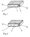
- 50 pieces of piezoceramic individual disks 1 with the dimensions 55 x 5.5 x 0.3, as shown in FIG. 1, are provided with metallizations (electrodes) 2 and then polarized.
- the disks are then stacked using a commercially available adhesive 4 and when pressure is applied.
- the adhesive 4 is dosed so that the joints created by the offset 6 are filled to about 50%.
- the side surfaces of the stack are cleaned. Subsequently, these side surfaces are metallized 5 using a sputtering process, so that all electrodes 2 which are pulled out on each side are connected to one another in an electrically conductive manner.
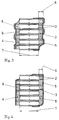
- the resulting stack with the dimensions 6 x 55 x 15 mm ( A x B x D ) (Fig. 5) is broken up into 10 individual stacks 10 of size 5 x 6 x 15 mm with a frame saw perpendicular to the side metallization 5.
- the individual stacks are wire-contacted and coated with a protective lacquer.
- the single stack expands in the field direction by approx. 20 ⁇ m.
- one or more strain gauges can be applied as strain sensors to the surfaces of the individual stacks 10 that are created during the sawing process for measurement and control purposes.
- piezoceramic foils with the dimensions 55 x 20 x 0.1 mm according to FIG. 2 metallized by a thick-film process with Ag paste with a layer thickness of 5 ⁇ m so that the insulation strips 3 (insulation on the pane surface) run parallel to the short side edges.
- the foils 1 are stacked in a staggered manner, being pressurized with an adhesive as a binder.
- the adhesive emerging from the gap between the individual foils completely fills the joints created during the offset stacking and also covers the protruding foil edges.
- the side edges of the stack are ground until the ceramic and the pulled-out electrodes 2 are ground.
- the side surfaces are metallized by a sputtering process with an Ag layer 5, which electrically connects the electrodes of the same polarity that are pulled out to one side.
- the stack with the dimensions 55.5 x 20 x 4 mm ( A x B x D ) (Fig. 6) is then in 6 individual stacks 10 of the dimensions 4 x 3 x 55.5 mm ( D x B1 x A ) disassembled. This creates a large number of individual stacks 10 with a small effective cross section (D x B1) and great effective length A.
- the translator stack performs a contraction perpendicular to the field direction (direction A) of approximately 45 ⁇ m when a direct voltage of 200 V is applied.
Applications Claiming Priority (1)
| Application Number | Priority Date | Filing Date | Title |
|---|---|---|---|
| DE4103657A DE4103657A1 (de) | 1991-02-07 | 1991-02-07 | Translatorstapel und verfahren zu dessen herstellung |
Publications (2)
| Publication Number | Publication Date |
|---|---|
| EP0576707A1 true EP0576707A1 (fr) | 1994-01-05 |
| EP0576707B1 EP0576707B1 (fr) | 1996-05-08 |
Family
ID=6424539
Family Applications (1)
| Application Number | Title | Priority Date | Filing Date |
|---|---|---|---|
| EP92111118A Expired - Lifetime EP0576707B1 (fr) | 1991-02-07 | 1992-07-01 | Empilement pour mouvement de translation et procédé de sa production |
Country Status (2)
| Country | Link |
|---|---|
| EP (1) | EP0576707B1 (fr) |
| DE (1) | DE4103657A1 (fr) |
Cited By (3)
| Publication number | Priority date | Publication date | Assignee | Title |
|---|---|---|---|---|
| WO2000034699A1 (fr) * | 1998-12-05 | 2000-06-15 | Robert Bosch Gmbh | Actionneur piezoelectrique |
| WO2003073523A2 (fr) * | 2002-02-22 | 2003-09-04 | Epcos Ag | Actionneur piezo-electrique a electrode externe structuree |
| CN110022085A (zh) * | 2019-05-21 | 2019-07-16 | 季华实验室 | 压电陶瓷叠堆同步粘接工装 |
Families Citing this family (1)
| Publication number | Priority date | Publication date | Assignee | Title |
|---|---|---|---|---|
| DE102005033463B3 (de) * | 2005-07-18 | 2007-02-01 | Siemens Ag | Piezoaktor |
Citations (2)
| Publication number | Priority date | Publication date | Assignee | Title |
|---|---|---|---|---|
| DE3330538A1 (de) * | 1983-08-24 | 1985-03-14 | Siemens AG, 1000 Berlin und 8000 München | Piezoelektrisches stellglied |
| US4978881A (en) * | 1988-07-20 | 1990-12-18 | Ngk Spark Plug Co., Ltd. | Piezoelectric actuator of lamination type |
-
1991
- 1991-02-07 DE DE4103657A patent/DE4103657A1/de not_active Withdrawn
-
1992
- 1992-07-01 EP EP92111118A patent/EP0576707B1/fr not_active Expired - Lifetime
Patent Citations (2)
| Publication number | Priority date | Publication date | Assignee | Title |
|---|---|---|---|---|
| DE3330538A1 (de) * | 1983-08-24 | 1985-03-14 | Siemens AG, 1000 Berlin und 8000 München | Piezoelektrisches stellglied |
| US4978881A (en) * | 1988-07-20 | 1990-12-18 | Ngk Spark Plug Co., Ltd. | Piezoelectric actuator of lamination type |
Non-Patent Citations (1)
| Title |
|---|
| PATENT ABSTRACTS OF JAPAN vol. 11, no. 110 (E-496)7. April 1987 & JP-A-61 258 485 ( AISAN IND CO LTD ) 15. November 1986 * |
Cited By (6)
| Publication number | Priority date | Publication date | Assignee | Title |
|---|---|---|---|---|
| WO2000034699A1 (fr) * | 1998-12-05 | 2000-06-15 | Robert Bosch Gmbh | Actionneur piezoelectrique |
| WO2003073523A2 (fr) * | 2002-02-22 | 2003-09-04 | Epcos Ag | Actionneur piezo-electrique a electrode externe structuree |
| WO2003073523A3 (fr) * | 2002-02-22 | 2004-02-19 | Epcos Ag | Actionneur piezo-electrique a electrode externe structuree |
| US7268471B2 (en) | 2002-02-22 | 2007-09-11 | Epcos Ag | Piezo actuator comprising a structured external electrode |
| CN110022085A (zh) * | 2019-05-21 | 2019-07-16 | 季华实验室 | 压电陶瓷叠堆同步粘接工装 |
| CN110022085B (zh) * | 2019-05-21 | 2020-03-27 | 季华实验室 | 压电陶瓷叠堆同步粘接工装 |
Also Published As
| Publication number | Publication date |
|---|---|
| EP0576707B1 (fr) | 1996-05-08 |
| DE4103657A1 (de) | 1992-08-13 |
Similar Documents
| Publication | Publication Date | Title |
|---|---|---|
| DE3214789C2 (fr) | ||
| EP0958620B1 (fr) | Actionneur piezo-electrique avec mise en contact d'un type nouveau et procede de fabrication dudit actionneur | |
| DE4202650C2 (de) | Piezoelektrische bimorphe Einrichtung und Verfahren zum Treiben einer piezoelektrischen bimorphen Einrichtung | |
| DE4201937C2 (de) | Piezoelektrisches laminiertes Stellglied | |
| EP1008193B1 (fr) | Procede de production d'actionneurs piezo-electriques, et actionneur piezo-electrique | |
| EP0947002A1 (fr) | Element d'entrainement ou de reglage piezo-electrique | |
| DE1208368B (de) | Piezoelektrischer Kraftmesser | |
| WO2007087912A1 (fr) | Procédé de mise en contact électrique d'un composant électronique | |
| EP0006624A2 (fr) | Méthode pour fabriquer des transducteurs ultrasoniques | |
| EP0050791B1 (fr) | Organe de réglage à commande électrique | |
| DE3330538A1 (de) | Piezoelektrisches stellglied | |
| DE3211539A1 (de) | Mehrschichten-stromschine hoher kapazitanz und verfahren zur herstellung derselben | |
| WO2005075113A1 (fr) | Convertisseur a ultrasons comportant un element convertisseur piezoelectrique, procede de fabrication de l'element convertisseur et utilisation du convertisseur a ultrasons | |
| EP0576707B1 (fr) | Empilement pour mouvement de translation et procédé de sa production | |
| DE3434729C2 (fr) | ||
| DE10021919C2 (de) | Verfahren zur Herstellung monolithischer piezokeramischer Vielschichtaktoren sowie monolithischer piezokeramischer Vielschichtaktor | |
| DE102006051080A1 (de) | Vielschichtaktoren mit Interdigitalelektroden | |
| EP0101999A1 (fr) | Coupleur piézo-électrique, en particulier un coupleur électro-mécanique d'allumage | |
| EP1129493B1 (fr) | Structure multicouche piezoceramique presentant une surface de section polygonale | |
| DE2938542C2 (de) | Signalzuführungsanordnung für ein Oberflächenwellen-Bauteil | |
| EP2054951B1 (fr) | Composant piézoélectrique | |
| EP0545391A1 (fr) | Organe d'actionnement comportant des disques céramiques ferroélectriques | |
| DE112010002244T5 (de) | Piezoelektrische gestapelte Stellanordnung | |
| DE102004056754A1 (de) | Piezoelektrisches Biegeelement | |
| DE10017331C1 (de) | Piezoelektrischer Vielschichtaktuator und Verfahren zu seiner Herstellung |
Legal Events
| Date | Code | Title | Description |
|---|---|---|---|
| PUAI | Public reference made under article 153(3) epc to a published international application that has entered the european phase |
Free format text: ORIGINAL CODE: 0009012 |
|
| AK | Designated contracting states |
Kind code of ref document: A1 Designated state(s): CH DK FR GB GR IT LI NL |
|
| 17P | Request for examination filed |
Effective date: 19940621 |
|
| 17Q | First examination report despatched |
Effective date: 19950426 |
|
| RAP1 | Party data changed (applicant data changed or rights of an application transferred) |
Owner name: TRIDELTA GMBH |
|
| GRAA | (expected) grant |
Free format text: ORIGINAL CODE: 0009210 |
|
| AK | Designated contracting states |
Kind code of ref document: B1 Designated state(s): CH DK FR GB GR IT LI NL |
|
| PG25 | Lapsed in a contracting state [announced via postgrant information from national office to epo] |
Ref country code: IT Free format text: LAPSE BECAUSE OF FAILURE TO SUBMIT A TRANSLATION OF THE DESCRIPTION OR TO PAY THE FEE WITHIN THE PRE;WARNING: LAPSES OF ITALIAN PATENTS WITH EFFECTIVE DATE BEFORE 2007 MAY HAVE OCCURRED AT ANY TIME BEFORE 2007. THE CORRECT EFFECTIVE DATE MAY BE DIFFERENT FROM THE ONE RECORDED.SCRIBED TIME-LIMIT Effective date: 19960508 Ref country code: NL Free format text: LAPSE BECAUSE OF FAILURE TO SUBMIT A TRANSLATION OF THE DESCRIPTION OR TO PAY THE FEE WITHIN THE PRESCRIBED TIME-LIMIT Effective date: 19960508 Ref country code: GB Effective date: 19960508 Ref country code: DK Effective date: 19960508 Ref country code: FR Effective date: 19960508 Ref country code: GR Free format text: LAPSE BECAUSE OF FAILURE TO SUBMIT A TRANSLATION OF THE DESCRIPTION OR TO PAY THE FEE WITHIN THE PRESCRIBED TIME-LIMIT Effective date: 19960508 |
|
| PG25 | Lapsed in a contracting state [announced via postgrant information from national office to epo] |
Ref country code: CH Effective date: 19960731 Ref country code: LI Effective date: 19960731 |
|
| GRAH | Despatch of communication of intention to grant a patent |
Free format text: ORIGINAL CODE: EPIDOS IGRA |
|
| NLV1 | Nl: lapsed or annulled due to failure to fulfill the requirements of art. 29p and 29m of the patents act | ||
| EN | Fr: translation not filed | ||
| GBV | Gb: ep patent (uk) treated as always having been void in accordance with gb section 77(7)/1977 [no translation filed] |
Effective date: 19960508 |
|
| PLBE | No opposition filed within time limit |
Free format text: ORIGINAL CODE: 0009261 |
|
| REG | Reference to a national code |
Ref country code: CH Ref legal event code: PL |
|
| STAA | Information on the status of an ep patent application or granted ep patent |
Free format text: STATUS: NO OPPOSITION FILED WITHIN TIME LIMIT |
|
| 26N | No opposition filed |