EP0576707A1 - Stack for translational movement and method of making the same - Google Patents
Stack for translational movement and method of making the same Download PDFInfo
- Publication number
- EP0576707A1 EP0576707A1 EP92111118A EP92111118A EP0576707A1 EP 0576707 A1 EP0576707 A1 EP 0576707A1 EP 92111118 A EP92111118 A EP 92111118A EP 92111118 A EP92111118 A EP 92111118A EP 0576707 A1 EP0576707 A1 EP 0576707A1
- Authority
- EP
- European Patent Office
- Prior art keywords
- stack
- disks
- translator
- individual
- electrodes
- Prior art date
- Legal status (The legal status is an assumption and is not a legal conclusion. Google has not performed a legal analysis and makes no representation as to the accuracy of the status listed.)
- Granted
Links
Images

Classifications
-
- H—ELECTRICITY
- H10—SEMICONDUCTOR DEVICES; ELECTRIC SOLID-STATE DEVICES NOT OTHERWISE PROVIDED FOR
- H10N—ELECTRIC SOLID-STATE DEVICES NOT OTHERWISE PROVIDED FOR
- H10N30/00—Piezoelectric or electrostrictive devices
- H10N30/80—Constructional details
- H10N30/87—Electrodes or interconnections, e.g. leads or terminals
- H10N30/871—Single-layered electrodes of multilayer piezoelectric or electrostrictive devices, e.g. internal electrodes
-
- H—ELECTRICITY
- H10—SEMICONDUCTOR DEVICES; ELECTRIC SOLID-STATE DEVICES NOT OTHERWISE PROVIDED FOR
- H10N—ELECTRIC SOLID-STATE DEVICES NOT OTHERWISE PROVIDED FOR
- H10N30/00—Piezoelectric or electrostrictive devices
- H10N30/01—Manufacture or treatment
- H10N30/08—Shaping or machining of piezoelectric or electrostrictive bodies
- H10N30/085—Shaping or machining of piezoelectric or electrostrictive bodies by machining
- H10N30/088—Shaping or machining of piezoelectric or electrostrictive bodies by machining by cutting or dicing
-
- H—ELECTRICITY
- H10—SEMICONDUCTOR DEVICES; ELECTRIC SOLID-STATE DEVICES NOT OTHERWISE PROVIDED FOR
- H10N—ELECTRIC SOLID-STATE DEVICES NOT OTHERWISE PROVIDED FOR
- H10N30/00—Piezoelectric or electrostrictive devices
- H10N30/80—Constructional details
- H10N30/87—Electrodes or interconnections, e.g. leads or terminals
- H10N30/872—Connection electrodes of multilayer piezoelectric or electrostrictive devices, e.g. external electrodes
Landscapes
- Engineering & Computer Science (AREA)
- Manufacturing & Machinery (AREA)
- General Electrical Machinery Utilizing Piezoelectricity, Electrostriction Or Magnetostriction (AREA)
Abstract
Description
Die Erfindung betrifft einen Translatorstapel, der aus einer Vielzahl von piezokeramischen Scheiben, die mit Oberflächenmetallisierungen als Elektroden versehen sind, besteht. Gleichzeitig beinhaltet die Erfindung ein Verfahren zum Herstellen eines Translatorstapels.The invention relates to a translator stack which consists of a multiplicity of piezoceramic disks which are provided with surface metallizations as electrodes. At the same time, the invention includes a method for producing a translator stack.
Es sind einige Möglichkeiten der Elektrodengestaltung für die einzelnen Scheiben bekannt. Ganzflächige Metallisierungen der gegenüberliegenden Hauptflächen führt notwendigerweise entweder zu aufwendigen Maßnahmen bei der äußeren Parallelschaltung gleichsinnig angesteuerter Elektroden (DE 321 8576) oder zu aufwendigen Isolationsmaßnahmen auf der Bauelementekante, z.B. bei monolithischen Vielschichtaktuatoren.There are some known electrode design options for the individual disks. All-over metallization of the opposite main surfaces necessarily leads either to complex measures for the external parallel connection of electrodes driven in the same direction (DE 321 8576) or to complex insulation measures on the component edge, e.g. in monolithic multi-layer actuators.
Um diese Nichteile zu vermeiden, wird in der DE-OS 333 0538 eine Metallisierung der Einzelscheiben derart vorgeschlagen, daß eine Flächenelektrode jeweils auf die gegenüberliegende Seitenkante herumreicht. Dies bedingt einen elektrodenfreien Streifen auf jeder Hauptfläche der Scheibe, der jeweils die Isolation der Elektroden zueinander gewährleistet.In order to avoid these non-parts, a metallization of the individual disks is proposed in DE-OS 333 0538 in such a way that a surface electrode extends around the opposite side edge. This requires an electrode-free strip on each main surface of the pane, which ensures that the electrodes are insulated from one another.
In diesen Bereichen treten beim elektrischen Ansteuern der Scheiben Felddeformationen auf, die zu einer geringeren Dehnung bzw. sogar zu Kontraktionen in Richtung der Wirkachse des Stapels führen. Die Folge davon sind hohe innere mechanische Spannungen zwischen regulär kontaktierten Gebieten, in denen das elektrische Feld parallel zur Wirkachse des Stapels verläuft, und den Gebicten der Isolierstreifen, in denen die Feldrichtung von der Wirkachse abweicht.In these areas, field deformations occur when the disks are electrically controlled, which lead to less elongation or even contractions in the direction of the effective axis of the stack. The consequence of this is high internal mechanical stresses between regularly contacted areas, in which the electric field runs parallel to the active axis of the stack, and the areas of the insulating strips, in which the field direction deviates from the active axis.
Diese mechanische Spannungen führen bei Betrieb des Translatorstapels, wie schon angedeutet, zu Energie- und Dehnungsverlusten, zu Inhomogenitäten der Dehnung über den Wirkquerschnitt, zu Verlusten an Steifigkeit und im Extremfall, z.B. bei hochdynamischem Betrieb, zur Zerstörung des Verbundes.As already indicated, these mechanical stresses lead to energy and elongation losses during operation of the translator stack, to inhomogeneities of the elongation across the effective cross section, to losses in rigidity and in extreme cases, e.g. in highly dynamic operation, to destroy the network.
Die Aufgabe der Erfindung besteht daher darin, einen Stapelaufbau anzugeben, der einerseits den Aufwand für eine äußere Verschaltung bzw. Elektkrodenisolation, der bei ganzflächiger Metallisierung der Hauptflächen der Einzelscheiben entsteht, vermindert und andererseits die beschriebenen Nachteile, die mit der Anordnung der Isolationsstreifen auf den Hauptflächen der Scheiben auftreten, vermeidet. Die Erfindung soll insbesondere für kleine Scheibendicken (<0,3 mm) eine kostengünstige Fertigung erlauben.The object of the invention is therefore to provide a stack structure which on the one hand reduces the outlay for external wiring or electrode insulation which arises when the main surfaces of the individual panes are metallized over the entire area, and on the other hand reduces the disadvantages described with the arrangement of the insulation strips on the main surfaces of the disks. The invention is intended to allow cost-effective production, in particular for small pane thicknesses (<0.3 mm).
Aufgabe der Erfindung ist es weiterhin, ein Verfahren zur Herstellung eines Translatorstapels anzugeben, das gewährleistet, daß Stapel auf effektiver Weise in den benötigten Abmessungen und Eigenschaften bereitgestellt werden können.It is also an object of the invention to provide a method for producing a translator stack which ensures that stacks can be provided in the required dimensions and properties in an effective manner.
Diese Aufgabe wird, wie in den Ansprüchen 1 bis 6 beschrieben, gelöst.This object is achieved as described in
Weitere Erläuterungen der Erfindungen gehen aus den nachfolgenden auf der Basis der Zeichnungen beschriebenen Ausführungsbeispielen hervor.Further explanations of the inventions emerge from the following exemplary embodiments described on the basis of the drawings.
Es zeigen:
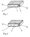
- Fig. 1:
- eine Einzelscheibe mit einer erfindungsgemäßen Metallisierung
- Fig. 2:
- eine Einzelscheibe mit einer weiteren erfindungsgemäßen Metallisierung
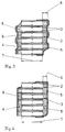
- Fig. 3:
- eine Schnittdarstellung eines erfindungsgemäßen Stapels in Trennrichtung bei Verwendung von Scheiben nach Fig. 1
- Fig. 4:
- eine Schnittdarstellung eines erfindungsgemäßen Stapels in Trennrichtung bei Verwendung von Scheiben nach Fig. 2
- Fig. 5:
- eine Prinzipdarstellung zur Trennung des ursprünglichen Stapels gemäß
Beispiel 1 und Fig. 3 - Fig. 6:
- eine Prinzipdarstellung zur Trennung des ursprünglichen Stapels gemäß
Beispiel 2 und Fig. 4.
- Fig. 1:
- a single disc with a metallization according to the invention
- Fig. 2:
- a single pane with a further metallization according to the invention
- Fig. 3:
- 2 shows a sectional illustration of a stack according to the invention in the separating direction when using disks according to FIG. 1
- Fig. 4:
- 3 shows a sectional illustration of a stack according to the invention in the separating direction when using disks according to FIG. 2
- Fig. 5:
- a schematic diagram for separating the original stack according to Example 1 and FIG. 3
- Fig. 6:
- a schematic diagram for separating the original stack according to Example 2 and FIG. 4.
Die in den Fig. 5 und 6 angedeuteten Pfeile sollen die Richtung des elektrischen Feldes bei Betrieb des Stapels verdeutlichen, wobei auch die weiter unten beschriebenen Einzelstapel gemeint sind.The arrows indicated in FIGS. 5 and 6 are intended to clarify the direction of the electrical field when the stack is in operation, which also means the individual stacks described below.
Die Stapelung der Scheiben 1 erfolgt so, daß das Gebiet mit irregulärer Feldverteilung 8 sich außerhalb des quasimonolithischen Wirkquerschnittes 7 befindet und dort nur die Funktion des Trägers der Metallisierungen 2; 5 hat.The
Die Fig. 1 und 2 zeigen dabei die zwei Möglichkeiten der Metallisierung (Elektroden), um den beabsichtigten Versatz 6 bei der Stapelung der Scheiben 1 realisieren zu können.1 and 2 show the two possibilities of metallization (electrodes) in order to be able to implement the intended
Die Herstellung des Stapelverbundes geschieht durch Verklebung und zwar derart, daß eine galvanische Kontaktgabe benachbarter Elektroden 2 erfolgt und nur eine dieser Elektroden nach außen geführt und jeweils mit den anderen herausgeführten Elektroden gleicher Polarität durch eine elektrisch leitende Beschichtung 5 miteinander verbunden wird. Die bevorzugte Verwendung des Klebers zur Füllung der beim versetzten Stapeln entstehenden spaltförmigen Vertiefungen wird anschließend in den beiden Beispielen beschrieben. Die mechanische Steifigkeit des ausgehärteten Klebers muß im Vergleich zu der der Keramik vernachlässigbar sein.The stack assembly is produced by gluing in such a way that galvanic contact is made between
Es werden 50 Stück piezokeramische Einzelscheiben 1 mit den Abmessungen 55 x 5,5 x 0,3, wie in Fig. 1 dargestellt, mit Metallisierungen (Elektroden) 2 versehen und anschließend polarisiert. Danach erfolgt die Stapelung der Scheiben unter Einsatz eines handelsüblichen Klebers 4 und bei Anwendung von Druck. Der Kleber 4 wird dabei so dosiert, daß die durch den Versatz 6 entstandenen Fugen zu etwa 50 % gefüllt werden. Nach dem Aushärten des Klebers bei 120oC erfolgt eine Reinigung der Seitenflächen des Stapels. Anschließend werden diese Seitenflächen mit einem Sputterverfahren metallisiert 5, so daß alle nach jeweils einer Seite herausgezogenen Elektroden 2 elektrisch leitend miteinander verbunden werden.50 pieces of piezoceramic
Der entstandene Stapel mit den Abmessungen 6 x 55 x 15 mm ( ![]()
![]()
Beim Anlegen einer Gleichspannung von 600 V führt der Einzelstapel eine Dehnung in Feldrichtung von ca. 20 µm aus.When a direct voltage of 600 V is applied, the single stack expands in the field direction by approx. 20 µm.
Auf die beim Trennsägen entstehenden Flächen der Einzelstapel 10 können nach einem Waschvorgang ein oder mehrere Dehnmeßstreifen als Dehnungssensor zu Meß- und Regelzwecken aufgebracht werden.After washing, one or more strain gauges can be applied as strain sensors to the surfaces of the
Es werden 40 piezokeramische Folien der Abmessung 55 x 20 x 0,1 mm gemäß Fig. 2 durch ein Dickschichtverfahren mit Ag-Paste der Schichtdicke 5 µm so metallisiert, daß die Isolationsstreifen 3 (Isolation auf der Scheibenfläche) parallel zu den kurzen Seitenkanten verlaufen.
Die Folien 1 werden wie in Fig. 4 dargestellt, versetzt gestapelt, wobei sie mit einem Kleber als Bindemittel unter Druck verfügt werden. Der aus dem Spalt zwischen den einzelnen Folien austretende Kleber füllt die beim versetzten Stapeln entstandenen Fugen voilständig und bedeckt auch die hervorstehenden Folienkanten.There are 40 piezoceramic foils with the dimensions 55 x 20 x 0.1 mm according to FIG. 2 metallized by a thick-film process with Ag paste with a layer thickness of 5 μm so that the insulation strips 3 (insulation on the pane surface) run parallel to the short side edges.
As shown in FIG. 4, the
Nach dem Aushärten des Klebers bei 120oC werden die Seitenkanten des Stapels überschliffen, bis die Keramik und die herausgezogenen Elektroden 2 angeschliffen sind. Nach einem Waschvorgang werden die Seitenflächen durch ein Sputterverfahren mit einer Ag-Schicht 5 metallisiert, die die jeweils nach einer Seite herausgezogenen Elektroden gleicher Polarität elektrisch miteinander verbindet.After the adhesive has hardened at 120 ° C., the side edges of the stack are ground until the ceramic and the pulled-out
Der Stapel mit den Abmessungen 55,5 x 20 x 4 mm ( ![]()
![]()
![]()
![]()
Nach dem Abschluß von Kontaktdrähten und Endstücken an die kleinen Seitenflächen der nun entstandenen Einzelstapel 10 werden diese polarisiert. Der Translatorstapel führt beim Anlegen einer Gleichspannung von 200 V eine Kontraktion senkrecht zur Feldrichtung (Richtung A) von etwa 45 µm aus.After the contact wires and end pieces have been terminated on the small side faces of the
Claims (6)
Applications Claiming Priority (1)
| Application Number | Priority Date | Filing Date | Title |
|---|---|---|---|
| DE4103657A DE4103657A1 (en) | 1991-02-07 | 1991-02-07 | TRANSLATOR STACK AND METHOD FOR THE PRODUCTION THEREOF |
Publications (2)
| Publication Number | Publication Date |
|---|---|
| EP0576707A1 true EP0576707A1 (en) | 1994-01-05 |
| EP0576707B1 EP0576707B1 (en) | 1996-05-08 |
Family
ID=6424539
Family Applications (1)
| Application Number | Title | Priority Date | Filing Date |
|---|---|---|---|
| EP92111118A Expired - Lifetime EP0576707B1 (en) | 1991-02-07 | 1992-07-01 | Stack for translational movement and method of making the same |
Country Status (2)
| Country | Link |
|---|---|
| EP (1) | EP0576707B1 (en) |
| DE (1) | DE4103657A1 (en) |
Cited By (3)
| Publication number | Priority date | Publication date | Assignee | Title |
|---|---|---|---|---|
| WO2000034699A1 (en) * | 1998-12-05 | 2000-06-15 | Robert Bosch Gmbh | Piezoelectric actuator |
| WO2003073523A2 (en) * | 2002-02-22 | 2003-09-04 | Epcos Ag | Piezo actuator comprising a structured external electrode |
| CN110022085A (en) * | 2019-05-21 | 2019-07-16 | 季华实验室 | Piezoelectric element synchronizes adhesive tool |
Families Citing this family (1)
| Publication number | Priority date | Publication date | Assignee | Title |
|---|---|---|---|---|
| DE102005033463B3 (en) * | 2005-07-18 | 2007-02-01 | Siemens Ag | piezo actuator |
Citations (2)
| Publication number | Priority date | Publication date | Assignee | Title |
|---|---|---|---|---|
| DE3330538A1 (en) * | 1983-08-24 | 1985-03-14 | Siemens AG, 1000 Berlin und 8000 München | Piezoelectric actuator |
| US4978881A (en) * | 1988-07-20 | 1990-12-18 | Ngk Spark Plug Co., Ltd. | Piezoelectric actuator of lamination type |
-
1991
- 1991-02-07 DE DE4103657A patent/DE4103657A1/en not_active Withdrawn
-
1992
- 1992-07-01 EP EP92111118A patent/EP0576707B1/en not_active Expired - Lifetime
Patent Citations (2)
| Publication number | Priority date | Publication date | Assignee | Title |
|---|---|---|---|---|
| DE3330538A1 (en) * | 1983-08-24 | 1985-03-14 | Siemens AG, 1000 Berlin und 8000 München | Piezoelectric actuator |
| US4978881A (en) * | 1988-07-20 | 1990-12-18 | Ngk Spark Plug Co., Ltd. | Piezoelectric actuator of lamination type |
Non-Patent Citations (1)
| Title |
|---|
| PATENT ABSTRACTS OF JAPAN vol. 11, no. 110 (E-496)7. April 1987 & JP-A-61 258 485 ( AISAN IND CO LTD ) 15. November 1986 * |
Cited By (6)
| Publication number | Priority date | Publication date | Assignee | Title |
|---|---|---|---|---|
| WO2000034699A1 (en) * | 1998-12-05 | 2000-06-15 | Robert Bosch Gmbh | Piezoelectric actuator |
| WO2003073523A2 (en) * | 2002-02-22 | 2003-09-04 | Epcos Ag | Piezo actuator comprising a structured external electrode |
| WO2003073523A3 (en) * | 2002-02-22 | 2004-02-19 | Epcos Ag | Piezo actuator comprising a structured external electrode |
| US7268471B2 (en) | 2002-02-22 | 2007-09-11 | Epcos Ag | Piezo actuator comprising a structured external electrode |
| CN110022085A (en) * | 2019-05-21 | 2019-07-16 | 季华实验室 | Piezoelectric element synchronizes adhesive tool |
| CN110022085B (en) * | 2019-05-21 | 2020-03-27 | 季华实验室 | Synchronous bonding tool for piezoelectric ceramic stacks |
Also Published As
| Publication number | Publication date |
|---|---|
| EP0576707B1 (en) | 1996-05-08 |
| DE4103657A1 (en) | 1992-08-13 |
Similar Documents
| Publication | Publication Date | Title |
|---|---|---|
| EP0958620B1 (en) | Piezo electric actuator with a new type of contacting and a method for the production thereof | |
| DE4202650C2 (en) | Piezoelectric bimorph device and method for driving a piezoelectric bimorph device | |
| DE4201937C2 (en) | Piezoelectric laminated actuator | |
| EP1008193B1 (en) | Method for the production of piezoelectric actuators and a piezoelectric actuator | |
| EP0947002A1 (en) | Piezo-electric driving or adjusting element | |
| DE1208368B (en) | Piezoelectric force meter | |
| WO2007087912A1 (en) | Method for making electrical contact with an electronic component | |
| EP0006624A2 (en) | Method for manufacturing ultrasonic transducers | |
| EP0050791B1 (en) | Electrically operated regulating unit | |
| DE3330538A1 (en) | Piezoelectric actuator | |
| WO2001084642A1 (en) | Piezo-ceramic multilayer component for measuring instruments and method for the production thereof | |
| DE3211539A1 (en) | HIGH-CAPACITY MULTI-LAYER GENERATOR AND METHOD FOR PRODUCING THE SAME | |
| WO2005075113A1 (en) | Ultrasound converter with a piezoelectric converter element, method for the production of said untrasound converter and use of said ultrasonic converter | |
| EP0576707B1 (en) | Stack for translational movement and method of making the same | |
| DE3434729C2 (en) | ||
| DE10021919C2 (en) | Process for producing monolithic piezoceramic multilayer actuators and monolithic piezoceramic multilayer actuators | |
| DE102006051080A1 (en) | Multilayer actuators with interdigital electrodes | |
| EP0101999A1 (en) | Piezo-electric coupler, in particular an electromechanical ignition coupler | |
| EP1129493B1 (en) | Piezoceramic multi-layer structure with regular polygon cross-sectional area | |
| DE2938542C2 (en) | Signal feed arrangement for a surface acoustic wave component | |
| EP2054951B1 (en) | Piezoelectric component | |
| EP0545391A1 (en) | Actuator composed of ferroelectric ceramic discs | |
| DE112010002244T5 (en) | Piezoelectric stacked actuator assembly | |
| DE102004056754A1 (en) | Piezoelectric bending unit for actuators and sensors, has two material plies that are connected to each other, where contact surface of the plies are evenly curved and geometrically compactly wound | |
| DE10017331C1 (en) | Multi-layer piezoelectric actuator e.g. for automobile, aircraft or spacecraft, has inner electrodes within piezoceramic layer stack coupled to outer electrodes via electrically conductive powder layer |
Legal Events
| Date | Code | Title | Description |
|---|---|---|---|
| PUAI | Public reference made under article 153(3) epc to a published international application that has entered the european phase |
Free format text: ORIGINAL CODE: 0009012 |
|
| AK | Designated contracting states |
Kind code of ref document: A1 Designated state(s): CH DK FR GB GR IT LI NL |
|
| 17P | Request for examination filed |
Effective date: 19940621 |
|
| 17Q | First examination report despatched |
Effective date: 19950426 |
|
| RAP1 | Party data changed (applicant data changed or rights of an application transferred) |
Owner name: TRIDELTA GMBH |
|
| GRAA | (expected) grant |
Free format text: ORIGINAL CODE: 0009210 |
|
| AK | Designated contracting states |
Kind code of ref document: B1 Designated state(s): CH DK FR GB GR IT LI NL |
|
| PG25 | Lapsed in a contracting state [announced via postgrant information from national office to epo] |
Ref country code: IT Free format text: LAPSE BECAUSE OF FAILURE TO SUBMIT A TRANSLATION OF THE DESCRIPTION OR TO PAY THE FEE WITHIN THE PRE;WARNING: LAPSES OF ITALIAN PATENTS WITH EFFECTIVE DATE BEFORE 2007 MAY HAVE OCCURRED AT ANY TIME BEFORE 2007. THE CORRECT EFFECTIVE DATE MAY BE DIFFERENT FROM THE ONE RECORDED.SCRIBED TIME-LIMIT Effective date: 19960508 Ref country code: NL Free format text: LAPSE BECAUSE OF FAILURE TO SUBMIT A TRANSLATION OF THE DESCRIPTION OR TO PAY THE FEE WITHIN THE PRESCRIBED TIME-LIMIT Effective date: 19960508 Ref country code: GB Effective date: 19960508 Ref country code: DK Effective date: 19960508 Ref country code: FR Effective date: 19960508 Ref country code: GR Free format text: LAPSE BECAUSE OF FAILURE TO SUBMIT A TRANSLATION OF THE DESCRIPTION OR TO PAY THE FEE WITHIN THE PRESCRIBED TIME-LIMIT Effective date: 19960508 |
|
| PG25 | Lapsed in a contracting state [announced via postgrant information from national office to epo] |
Ref country code: CH Effective date: 19960731 Ref country code: LI Effective date: 19960731 |
|
| GRAH | Despatch of communication of intention to grant a patent |
Free format text: ORIGINAL CODE: EPIDOS IGRA |
|
| NLV1 | Nl: lapsed or annulled due to failure to fulfill the requirements of art. 29p and 29m of the patents act | ||
| EN | Fr: translation not filed | ||
| GBV | Gb: ep patent (uk) treated as always having been void in accordance with gb section 77(7)/1977 [no translation filed] |
Effective date: 19960508 |
|
| PLBE | No opposition filed within time limit |
Free format text: ORIGINAL CODE: 0009261 |
|
| REG | Reference to a national code |
Ref country code: CH Ref legal event code: PL |
|
| STAA | Information on the status of an ep patent application or granted ep patent |
Free format text: STATUS: NO OPPOSITION FILED WITHIN TIME LIMIT |
|
| 26N | No opposition filed |