EP0574111B1 - Effets d'illumination pour un système numérique d'effets vidéo - Google Patents
Effets d'illumination pour un système numérique d'effets vidéo Download PDFInfo
- Publication number
- EP0574111B1 EP0574111B1 EP93301959A EP93301959A EP0574111B1 EP 0574111 B1 EP0574111 B1 EP 0574111B1 EP 93301959 A EP93301959 A EP 93301959A EP 93301959 A EP93301959 A EP 93301959A EP 0574111 B1 EP0574111 B1 EP 0574111B1
- Authority
- EP
- European Patent Office
- Prior art keywords
- tile
- pixel
- lighting
- pixels
- image
- Prior art date
- Legal status (The legal status is an assumption and is not a legal conclusion. Google has not performed a legal analysis and makes no representation as to the accuracy of the status listed.)
- Expired - Lifetime
Links
Images


Classifications
-
- H—ELECTRICITY
- H04—ELECTRIC COMMUNICATION TECHNIQUE
- H04N—PICTORIAL COMMUNICATION, e.g. TELEVISION
- H04N5/00—Details of television systems
- H04N5/222—Studio circuitry; Studio devices; Studio equipment
- H04N5/262—Studio circuits, e.g. for mixing, switching-over, change of character of image, other special effects ; Cameras specially adapted for the electronic generation of special effects
- H04N5/2628—Alteration of picture size, shape, position or orientation, e.g. zooming, rotation, rolling, perspective, translation
-
- G—PHYSICS
- G06—COMPUTING; CALCULATING OR COUNTING
- G06T—IMAGE DATA PROCESSING OR GENERATION, IN GENERAL
- G06T15/00—3D [Three Dimensional] image rendering
- G06T15/50—Lighting effects
- G06T15/80—Shading
- G06T15/83—Phong shading
Definitions
- This invention relates to a digital video effects system for the manipulation of pictures represented by video signals.
- it relates to the provision of lighting effects in such a system.
- the art of manipulating pictures represented by digital video signals is well established. In essence the manipulation is accomplished by: digitising an analogue video signal by sampling it and converting each sample into a binary word of, for example, 8 or 10 bits representing that sample; storing fields or frames of the digitised signal in memory; and controlling either the reading from or the writing to the memory so as to produce from each field or frame a picture that differs from that represented by the input video signal in that at least one geometrical parameter thereof is changed.
- Such geometrical parameter may, for example, comprise the location of the picture along one or more of up to three axes and/or the angular position of the picture about one or more axes.
- Other such parameters may comprise the size of the picture (in the horizontal and/or vertical direction thereof), the extent of shearing of the picture, and the perspective of the picture.
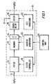
- FIG. 1 of the accompanying drawings shows in simplified block diagram form the general overview of a typical digital video effects system for effecting such manipulation of a picture.
- the general kind of apparatus now to be described with reference to Figure 1 has been embodied in a variety of known propriety items of digital video effects equipment, and the operation and construction thereof is well known to those skilled in the art.
- the digital video effects system comprises a digital video effects unit, which is designated 10 in Figure 1, and a control unit 24.
- a video signal V 1 representing a picture P 1 that is to be manipulated is input into the digital video effects unit 10 at 11.
- manipulation of the input picture P 1 is performed by controlling the read addresses to the memory 14, although write side address mapping is also known. This control of the read side addresses is effected by the address generator 20.
- a filter 12 is provided to compensate for the effects of compression.
- a filter controller 18 determines local scaling factors representative of the amount of compression for localised areas of the image, these local scaling factors being used to control the filter 12 to apply appropriate amounts of filtering to respective areas of the image.
- a pixel interpolator 14 can be provided to enable output pixel values to be computed where the address generator 20 does not generate a one-to-one mapping between a storage location in the memory 13 and the output pixels.
- a synchronisation delay 15 allows the data output from the memory 13 to be aligned with frame synchronisation information.
- a digital linear keyer 16 allows the data output from the memory 13 (which is representative of foreground information) to be keyed into the background (represented by a signal B input to keyer 16) for forming the output video V 2 of the output picture P 2 .
- a key processor 22 controls the operation of the digital linear keyer 16.
- the digital video effects unit 10 is under the control of the control unit 24 which can, but need not, be implemented as a conventional personal computer or a computer workstation with appropriate control software.
- a known example of a digital video effects system having the above architecture can perform 3D linear manipulations of high definition video with a very high video output quality.
- the known system is limited to linear manipulations of video, being unsuitable for providing video texture mapping, or free form modelling onto a non-linear surface.
- Video texture mapping is a term which derives from computer graphics where it is used to describe the mapping of an image onto a 3D surface. Originally this technique was developed for simulating surface texture, an appropriate image being mapped to give the desired effect. However, it has also been used for mapping other images to create other effects. See, for example, the colour plates in the book “Computer Graphics, Principles and Practice", Second Edition by Messrs Foley, Van Dam, Feiner and Hughes, published by Addison Wesley in 1990. In computer graphics applications, however, such video texture mapping is rarely, if ever, performed in real time.
- EP-A-0248626 discloses a video signal processing system which changes the shape of a video frame so that it appears to take the form of a three dimensional object. The system also applies shading to the object in response to an imaginary light source. The address data is processed to produce light intensity factors and the value of each pixel in each video frame is adjusted in response to a light intensity factor.
- An object of the present invention is to provide a digital video effects system which enables the generation of lighting effects in an efficient and cost effective manner.
- a digital video effects system for mapping a source video image comprising an array of pixels onto an object surface to produce an output image
- the system comprising a memory for temporarily storing an array of pixels derived from the source video image, control means for establishing a surface function defining the object surface, address means coupled to said control means for computing read addresses for mapping pixels from the memory to form output pixels representative of the source video image mapped onto the object surface, write-side lighting effect means for modifying pixels from the source video image before writing to the memory, characterised by mapping means for logically sectioning the source image into a plurality of tiles such that each tile corresponds to an array of pixels of the source image, the mapping means being responsive to surface function for computing a mapping of the tile corner coordinates onto the object surface.
- lighting processing is performed as a write-side process (i.e. it is performed on pixel values from the source video image before those values are stored in memory).
- Arranging for write-side processing in this manner enables lighting effects to be provided with a relatively small amount of hardware compared to that which would be required for read-side processing as part of a ray tracing technique.
- Write-side lighting in accordance with the invention can be applied for digital effects systems which provide mapping of a source video image onto a non-linear object surface.
- the invention is not limited to such mapping for non-linear object surfaces, and can be applied to digital video effects system providing mapping onto linear surfaces.
- the lighting effect means comprises a lighting effect processor which is responsive to lighting factors produced by a lighting factor generator.
- the lighting factor generator preferably comprises means for generating lighting factors for each pixel of each tile from mapped tile corner coordinate.
- the lighting factor generator is responsive to tile corner coordinates produced by the mapping means for generating a normal to each tile.
- the lighting factor generator preferably generates an interpolated normal for each pixel of the tiles from the surrounding tile normals.
- the lighting factor generator also computes pixel coordinates for the pixels of a tile as mapped onto the object surface by interpolation of the coordinates of the mapped tile corner points.
- the lighting factor generator preferably calculates an intensity multiplier for each pixel from the interpolated normal and coordinate of each pixel.
- the light effect means outputs pixels to a filter for filtering the pixels before storage in the memory, the filter applying variable filter characteristics in accordance with local scaling factors for the tiles to which the pixels belong.
- scale factor generating means responsive to the mapped tile corner coordinate values generated by the mapping means is provided for controlling the filter to perform appropriate filtering for respective tiles.
- the example of an image processing system in accordance with the invention to be described herein enables a source video image to be mapped in real time onto a 3D non-linear surface through the use of a ray-tracing technique.
- the object surface onto which the video image is to be mapped has to be defined.
- the object surface is defined in terms of the so-called "Bezier surfaces”.
- a Bezier curve is a two-dimensional curve constructed by forming a polynomial function from a set of control points.
- Bezier curve lies within the convex hull defined by the control points.
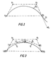
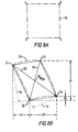
- Another important property of Bezier curves is that the tangent to the curve at an end point is along the line joining that end control point to the adjacent control point. In order, therefore, to ensure continuity between a first Bezier curve and a second Bezier curve at an end point it is merely necessary to ensure that the common end point of the two curves and the respective adjacent control points all lie on a straight line. This is illustrated in Figure 2 for the curves C 0 and C 1 and control points P 2 , P 3 , P 4 .
- FIG. 3 illustrates the generation of the control points for Bezier curves C 1 and C r , being Bezier curves formed by subdividing, by two, the Bezier curve C 0 .
- the control points for the left hand curve C 1 are L 0 , L 1 , L 2 and L 3 .
- the control points for the right hand curve C r are R 0 , R 1 , R 2 and R 3 .
- the two new Bezier curves can be generated from the original Bezier curve by simple additions and divisions by two. In a binary system, therefore, the new Bezier curves can be generated by a simple combination of additions and shift operations.
- a Bezier surface is defined by two sets of Bezier curves specified by appropriate input control points.
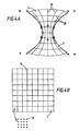
- Figure 4A shows a surface generated using this method with respect to control points represented by the small plus signs.
- the generally horizontal, gh, and generally vertical, gv, line segments in Figure 4A describe lines of constant latitude and longitude (u and v) over the surface for respective polynomials
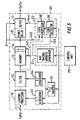
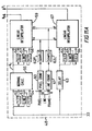
- FIG. 5 shows, in simplified block diagram form, an image processing system in accordance with the invention.
- a digital video effects unit 30 includes a video path similar to that in the prior art including a source image input 11, a filter 12, a memory 13 with a pixel interpolator 14, a synchronisation delay circuitry 15 and a digital keyer 17.
- the digital video effects unit 30 includes a lighting processor 19 which is arranged before the filter 12 and the memory 13 in the image processing path. In other words, the lighting processing is arranged as a write-side process with respect to the memory 13.
- the digital video effects unit 30 is under the control of a workstation 25.
- the workstation 25 is provided with software for defining an object onto which a source video image is to be mapped in terms of Bezier surface functions.
- the output of the workstation includes sets of co-ordinates for the Bezier control points for those surfaces (eg. the points P 0 , P 1 , P 2 and P 3 shown in Figure 2).
- a lighting factor (L.F) generator 33 is provided for controlling the operation of the lighting processor 19 .
- a scale factor (S.F) generator 34 controls the operation of the filter 12.
- the L.F and S.F generators are both responsive to a tile mapper 32.
- the tile mapper 32, and an address generator 21 and a key processor 23 for controlling the memory 13 and the keyer 17, respectively are specifically adapted to respond to Bezier control point data from the workstation 25 and will be explained in more detail hereinbelow.
- the tile mapper 32, the address generator 21 and the key processor 23 use the control points to control, respectively, the write side processing of the received images, the read-side addressing of the memory 13 and the operation of the keyer 17.
- the write-side processing of the received video images is controlled by processing the source image space as a rectangle made up of tiles t (a tile is an area of the source image space constructed from a group of individual pixels P).
- Figure 4B is a schematic representation of a simplified source image area, or space made up of an array of sub-areas in the form of 8 x 8 square tiles, t, each tile being made up of an array of 4 x 4 pixels, P.
- the tiles need not be square, and could be larger.
- the mapping of these tiles onto the desired shape is computed from the Bezier surface of the target object, specifically from the Bezier control points output by the workstation 25 as will be described later.
- the generally horizontal and generally vertical lines of constant latitude and longitude of the Bezier surface illustrated in Figure 4A could represent the mapping of the edges of the tiles of the source image space onto that surface. Note that there is a one-to-one mapping between each of the tiles of the source image space represented in Figure 4B and the corresponding mapped tiles on the Bezier surface illustrated in Figure 4A.
- tile mapper 32 of Figure 5 The purpose of the tile mapper 32 of Figure 5 is to compute the mappings of the corners of the tiles for the input space onto the target object surface.
- FIG. 6 is a schematic block diagram of the tile mapper 32, which includes control point storage 35, mapping logic 36 and mapping storage 37.
- the input to the tile mapper is in the form of an array of Bezier control points defining the target object, as output by the control unit 25. These control points are stored in control point storage 35.
- the target object will be defined in terms of a plurality of surface patches, each patch being itself defined in a Bezier surface function in terms of the control points for a constituent set of Bezier curve functions.
- the target object comprises a single patch defined in terms of a single set of sixteen control points.
- the mapping logic 36 determines, for each tile corner point in the tiled source image space, the mapping of that point into mapped space. In performing this processing, the mapping logic accesses the control points in the control point storage and stores the computed corner point mappings in the mapping storage 44.
- the mapping logic 42 processes each tile corner point in turn, computing for that corner point a mapped coordinate value. The processing of the mapping logic 42 is summarised in Figure 7.
- the mapping logic processes the tiles row-by-row, and within each row, column-by-column.
- the mapping logic starts at step 38 with treating the first, i.e. the top, horizontal edge of the top row of tiles, and selects, at step 39, the first vertical tile edge (i.e. the left hand tile edge).
- the mapping logic has selected the top left hand corner of the image.
- the mapping logic initialized variables x, y and z for accumulating the mapping for the point currently in question (i.e. initially the top left hand corner of the image).
- the mapping logic computes the mapping for the point in question by considering each control point in turn.
- the control points are stored in the memory as a two dimensional array of control points; the mapping logic 36 accessing this array of control points using variables j and k.
- the mapping logic initializes the variable j.
- the mapping logic initializes the variable k.
- the mapping logic evaluates the horizontal blending function for u and j to generate a horizontal blending value bu, and evaluates the vertical blending function for v and k to generate a vertical blending value, bv.
- the mapping logic updates the currently accumulated x, y and z values for the tile corner point in question.
- the new value for the x coordinate is computed by adding to the previous value of the variable x, the x coordinate value of the control point identified by the variables j, k multiplied by the horizontal blending value bu and the vertical blending value bv.
- the new value for the variable y is computed by adding to the previous value of the variable y, the y coordinate of the control point identified by the variables j and k multiplied by the horizontal blending value bu and the vertical blending value bv.
- the new value of the variable z is computed by adding to the previous value of the variable z, the z coordinate of the control point identified by the variables j and k multiplied by the horizontal blending value bu and the vertical blending value bv.
- the contribution of the coordinate values of each control point can be accumulated.
- the x, y and z values for that tile corner point can be stored in the mapping storage 37.
- the mapping logic determines whether there is another tile edge to be considered and if so the mapping logic determines the v value for this next tile edge and returns control to step 40 where the values for x, y and z are re-initialised for generating the mapping for this new point.
- the mapping logic continues to step along a line of tiles until the right hand edge of the last tile has been considered.
- the mapping logic then proceeds at step 47 to test whether there is another horizontal tile edge to be processed. If there is, the u value is updated accordingly and the next tile edge is considered. All of the vertical edges, including the top and the bottom edges will be processed so that mappings are generated for each corner point of the tiles of the source image space.
- mappings of corner points of the tiles are determined.
- the mapped coordinates of the corner points of the tiles are used by the lighting factor generator 33 to generate lighting factors for controlling the lighting processor 19.
- the differences between the original and mapped corner points for the tiles are used by the scaling factor generator 34 to determine local scaling factors for each of the tiles, which in turn are used to control the filter 12 for applying a degree of filtering to each tile of the source image appropriate to the compression effective for that tile as a result of the mapping.
- the lighting factor generator 33 utilizes the tile corner point generated by the tile mapper 32.
- Figure 8A shows a local area (specifically the tile labelled "ts" in Figure 4A) of the input image or picture, represented by the digital signal V 1 , prior to manipulation by mapping.
- the tile ts is square.
- the tile has corners a, b, c and d. Its edges c-d and b-a horizontal and its edges c-b and d-a are vertical.
- Figure 8B shows the tile ts of Figure 8A after manipulation as "Its".
- the positions of the corners a, b, c and d after manipulation, that is their positions in the manipulated image, are represented in Figure 8B as Ia, Ib, Ic and Id, respectively.
- Figure 8B also illustrates two vectors V1 and V2 defined with respect to pairs of corner points (Ib-Id and Ia-Ic), respectively, of the mapped tile and a normal vector N Its to the mapped tile.
- the normal N Its is defined as the dot product of the vectors V1 and V2.
- the write-side lighting processing of the present example of the invention uses the tile corner points to calculate a normal to each tile. By interpolation of the normals to each tile it is then possible to determine a normal vector for a mapping of each pixel by interpolation and to calculate lighting factors using the dot product of the calculated normals for the pixels and a lighting vector.
- N p represents a normal to a pixel on the surface of the object in question.
- L represents a lighting vector.
- the values Id, Ia, Kd and d0 ⁇ and the lighting vector L will be constant. However, new values for the normal to the pixel N and for the distance from the light source to the pixel will need to be calculated for each pixel of the image.
- the lighting factor generator 33 performs the calculation indicated by the above equation for the light intensity by calculating normals for each of the tiles from the corner points of those tiles and then interpolating between those normals to generate normals for each of the individual pixels.
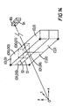
- Figure 9B represents this process in schematic terms for two dimensions, where S is the surface of the object in question, where N A , N B and N C represent normals to each of tiles A, B and C, respectively.
- N p represents a normal to a particular pixel from the tile which is computed by interpolation of the adjacent tile normals.
- Figure 9B represents the normals N A , N B and N C at the centre of the respective tiles.
- Figure 9C is a three dimensional representation of the tiles of the input image.
- the normal for tile T 00 , T 01 , T 10 , T 11 and so on, that is normals N 00 , N 01 , N 10 , N 11 , and so on, are defined at the top left corner of the corresponding tiles.
- the normals N p for each of the pixels P in each tile can be calculated by the normals at the four corners of that tile.
- the normals N p for each of the pixels in the top left hand tile can be computed by interpolating the values of the surrounding four normals N 00 , N 01 , N 10 and N 11 . The interpolation is performed in a linear manner using the displacements y and x from the top and left hand edges of the tile in question.
- normals are calculated for tiles which extend to the bottom and the right of the input video area (i.e. to the bottom and the right of the array of tiles ts shown in Figure 4B).
- the additional tiles to the right and the bottom are not shown in Figure 4B.
- a tile normal is generated for each corner of each of the tiles in the array of tiles shown in Figure 4B.
- These normals defined at the corners can then be used to compute a normal for each of the pixels within each of the tiles t shown in Figure 4B.
- a normal N p computed in this way can then be used as the normal N in the equation for light intensity mentioned above to form the dot product with the light vector L.
- the distance d from the light to the pixel also needs to be calculated for each pixel. This can also be calculated by interpolation from the coordinates of the mapping tile corner points which are output by the mapping logic 32.
- p x , p y and p z are the interpolated mapped coordinates of the pixel in question and l x , l y and l z are the coordinates of the light source.
- FIG 10 is a schematic block diagram illustrating, in more detail, the lighting factor generator 33 and the lighting processor 19.
- the lighting factor generator 33 comprises a normal/distance interpolator 48 and a lighting factor multiplier generator 49.
- the lighting processor 19 comprises a pixel multiplier 50 and a delay stage 51.
- FIG 11A is a schematic block diagram of the normal/pixel interpolator.
- the normal/pixel interpolator receives the tile corner coordinate from the tile mapper 32 and timing signals coordinated with the pixels of an input image.
- the tile coordinates need to be provided to the normal/pixel interpolator in advance of the pixels to which the interpolated values relate due to the manner of calculation of the interpolated normals and the interpolated pixel coordinates of the mapped pixels.
- the mapped tile corner coordinates are input to a normal calculation circuit 55 which forms the normal for each tile by forming the dot product of the vectors joining the opposite corner points of each tile as illustrated schematically in Figure 8B.
- the tile coordinates are supplied row by row and within each row corner by corner.
- the rate at which the tile corner coordinates are supplied depends on the number of pixels per tile. If, therefore, in the example shown in Figure 4B there are 16 pixels per tile, then a set of tile corner coordinates will be provided at one quarter of the pixel rate.
- the tile corner coordinate for each tile can be supplied simultaneously to the normal calculation circuit 55 by supplying a current tile coordinate (e.g. N 11 ) directly to the normal calculation, a second tile coordinate (e.g. N 10 ) with a one tile delay by means of a one tile delay means 52, a third pixel (e.g.
- the normal calculation circuit 55 generates the normal by computing the dot product of the vectors joining the diagonally opposite mapped tile corner point.
- This normal N c is then supplied to a linear interpolator 59.
- a linear interpolator 59 In order to compute the position of the pixels within a particular tile (e.g. tile T 00 ), it is necessary to already possess the normals for the four tile corner points of that tile.
- the tile corner points N c output by the normal calculation 55 are assumed to relate to the top left hand corner of the tile just calculated. Accordingly, a one line and one tile delay is necessary before all the corner points of a tile for which a normal has been calculated by the normal calculation unit 55 are available.
- a combination of means providing a one tile delay 56, a one line delay 57 and a further one tile delay 58 are provided in a similar manner to the delay units 52, 53 and 54 in order that the four tile corner point normals for a particular tile can be input simultaneously into the linear interpolator 59.
- the interpolation of the pixel normal for a pixel within the tile can then be calculated in accordance with the equation 7 above for the calculation of an interpolated normal N P .
- the linear interpolator 59 performs this calculation in response to x and y values supplied thereto.
- the x and y values are calculated by counting pixels along each row using a pixel counter 60 and counting the lines of pixels by a line counter 61.
- the pixel counter is clocked by a pixel count signal and is reset by a line count signal.
- the line counter is clocked by a line count signal and reset by a frame count signal. Circuits 62p and 62l sample, respectively, the lower significant bits of the counts output by the pixel counter 60 and the line counter 61, respectively.
- the circuits 62p and 62l sample the bottom two bits of the pixel and line counters whereby the values of x and y each cycle through zero, one, two, three in order to provide a linear interpolation of the normals input for the corner points of that tile. If another number of pixels where provided in each tile (e.g. 36), then the sampling circuits 62p and 62l would be arranged to sample the lower significant bits of the pixel count appropriately (e.g. modulo 6, whereby the values x and y would cycle between zero and five).
- the linear interpolator 59 outputs normals N p for respective pixels in response to the tile corner normals and the values of x and y input thereto in accordance with the equation for an interpolated normal N P referred to above.
- the tile corner coordinates are also supplied to circuitry for interpolating the mapped coordinates of the pixels of a tile.
- the tile coordinates are supplied to a delay stage 63 which provides a delay equal to that resulting from the circuitry 52, 53, 54 and 55 in the normal calculation circuitry.
- the output of the delay circuitry 63 is then supplied to a linear interpolator 67.
- delay means 64, 65 and 66 for providing a one tile delay, 64, a one line delay, 65, and a further one tile delay, 66 (compared the delay means 52, 53 and 54) the coordinates for the four mapped corners of a tile are supplied simultaneously to the linear interpolator 67.
- the linear interpolator 67 is responsive to the values of x and y output by the circuit 62p and 62l, respectively, to linearly interpolate the mapped corner points of the tile for generating mapped pixel coordinates for each pixel of the tile.
- the output pixel coordinates p i (x, y, z) are output from the normal/pixel interpolator 48 in synchronism with the corresponding normal N p for that pixel.
- Figure 11B is a schematic block diagram of the lighting factor multiplier circuit.
- the normal vector for a pixel N p is input to a circuit 68.
- the circuit 68 forms the dot product of the pixel normal N p and a lighting vector L supplied from the control unit 25.
- the interpolated pixel coordinates P i (x, y, z) are input to means for calculating the relation (Kd x Id)/(di + d0 ⁇ ). Accordingly, the circuit 69 also receives the coordinates of the light source L (x, y, z), the value of (Kd x Id) and d0 ⁇ . These values are provided from the control unit 25. The computation unit 69 then computes the relationship by computing the distance d i for the pixel in question from the coordinates of the interpolated pixel P i and the light source in accordance with the equations (8 or 9) for calculating d indicated above.
- the value of the relation (Kd x Id)/(di + d0 ⁇ ) can be calculated.
- the output of the units 68 and 69 for a pixel are supplied simultaneously to a multiplier 70 and subsequently to an adder 71, where the value Kd Ia is added (the value Kd Ia being supplied from the control unit 25) in order to generate the light intensity multiplier which forms the lighting factor for the current pixel.
- the lighting factor is used as a multiplier for multiplying the intensity of a received pixel in the pixel multiplier 50 of the pixel processor 19.
- the delay stage 51 in the received pixel line is arranged to delay received pixels by an appropriate amount such that the lighting factor for a pixel is output from the lighting factor generator 33 to the pixel multiplier 50 at the same time as the pixel concerned is supplied from the delay stage 51 to the pixel multiplier 50.
- the pixels with modified pixel intensity are output from the lighting processor 19 to the filter 12.
- the scale factor generator 34 which generates the scale factors for controlling the filter 12, uses the output of the tile mapper 32 in order to generate those scale factors.
- Figure 12 represents a local scaling factor computation means 34 which can compute a local horizontal scaling factor lh and a local vertical scaling factor lv for each tile of the source image where the tiles are mapped to form a quadrilateral which need only be generally in the shape of a parallelogram.
- a first computation section 72 computes values xv, xh, yv and yh from the coordinates of points Ia, Ib and Ic for each mapped tile, using the coordinates for those points stored in the mapping storage 44. These values, 74, are output to the second computation section 76. This second computation section computes the corresponding values of lh and lv using trigonometric relationships.
- the filter 12 is preferably a finite impulse response (FIR) filter.
- FIR finite impulse response
- the design of 2D FIR filters is known per se and therefore the preferred form of filter will not be described in great detail herein.
- a 2D FIR filter generally will comprise a plurality of multipliers supplied with respective weighting coefficients, a plurality of one sample delay elements and one line delay elements (line stores) arranged upstream or downstream or the multipliers to delay the samples of the input signal by different amounts to form the predetermined set or vertically and horizontally spaced samples, and a summing means to sum the delayed, weighted products.
- Figure 13 is a schematic representation of a suitable filter in a rather general and simplified form, the filter 12 comprising a plurality of multipliers 12M, a plurality of delay elements 12D and a summing means 12S. Respective different weighting coefficients are supplied to the multipliers 12M on lines extending from a bandwidth control means 12B.
- the bandwidth control means 12B is included in the filter 12 so that the values of the horizontal and vertical local scaling factors lh and lv can be used directly to compute appropriate values for the weighting coefficients to achieve a reduction in horizontal and vertical bandwidth of the filter 12.
- a range of sets of weighting coefficient values appropriate to all possible values of lh and lv is computed at the design stage and the bandwidth control means 82 is implemented in the form of PROM that stores a look-up table of the pre-computed sets of weighting coefficient values.
- the bandwidth control means can output appropriate values of the weighting coefficients to the multipliers 12M at each clock period in accordance with the values of lh and lv received from the local scaling factor computation means 34.
- the required reductions in horizontal and vertical bandwidths within a tile are related to the ratios of the horizontal and vertical dimensions and the amount of roll and shear of the manipulated tile compared to the unmanipulated image tile. These factors are taken into account in the design of the look-up table in the bandwidth control means 34, whereby the values lh and lv (rather than ratios computed therefrom) can be supplied directly to the bandwidth control means 34 as the horizontal and vertical local scaling factors.
- the filtering of the source image signals is arranged to be performed in real time in synchronism with the receipt of the source image samples from the lighting processor 19; the filtered source image samples being stored in the memory 13.
- delay means can be provided.
- the delay means can be inserted between the tile mapper 32 and the scale factor generation means 34, or between the scale factor generation means 34 and the filter 12.
- the required delay can be determined by one skilled in the art dependant on the specific circuit delays in any particular implementation. It can also be the case in specific implementations that no further delay is required between the tile mapper 32 and the filter 12, but alternatively that further delay means are required between the tile mapper 32 and the lighting processor 19. It is within the scope of the person skilled in the art provide appropriate timing of the signals for controlling the lighting processor 19 and the filter 12.
- the filtered image when is stored in the memory 13 in the received sequence, can then be mapped onto the target object by generating appropriate memory read addresses.
- the address generator 21 does this using a ray tracing sub-division technique known a Bezier subdivision.
- the technique used relies on the fact, mentioned earlier, that Bezier curves can easily be sub-divided into two curves by simple operations on the control points which only require additions and divisions by two.
- the purpose of the address generator 21 is to generate address data defining the location of filtered source image data in the memory 15 which can be used to generate each pixel of the object image for subsequently forming the output image.
- the process is based on the concept of generating a ray for each object image pixel and detecting whether that ray intersects the object, and if so to determine one or more storage locations in the memory 13 containing source image data to be used to form the object pixel for that ray.
- the technique involves, for each ray, recursively sub-dividing the Bezier surface or patch into quadrants.
- the control points can be used to define a convex hull which completely contains the curve.
- the address generator uses a simpler "bounding box" based on the maximum and minimum of the x and y components, respectively, of the control points.
- the so-called "bounding box” is arranged to contain the surface patch and to be aligned with the coordinate axes.
- the address generator computes whether the ray intersects this bounding box. The subdivision process continues until a desired resolution is obtained.
- each of the rays starts from an origin '0' and passes through object space.
- Figure 14 illustrates a situation where an intersection has been established for the top left bounding box from the first subdivision S1 and a second subdivision S2 has been made within this bounding box as indicated by the dotted lines. This process continues until the desired resolution or accuracy has been achieved (here at subdivision Sn), and a result sub-patch RS can be determined.
- the rays for respective pixels diverge from the origin 'O'.
- such a diverging ray system provides severe processing penalties when testing whether an intersection between a ray and a bounding box has occurred.
- the preferred embodiment of the invention uses an approximation to the diverging ray approach in which parallel rays are employed, as will be described later.
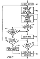
- Figure 14 is a flow diagram setting out the basic steps in the subdivision process.
- a depth value is set in a register at step 80.
- the original patch is subdivided into four sub-patches by the appropriate calculations on the original control points, and the control points for the sub-patches are stored on a stack.
- the control points (x, y and z values) for each sub-patch are variables for assembling u, v and z values for that sub-patch.
- control points for the first sub-patch on the stack are taken at step 84 and a bounding box is computed for this sub-patch.
- a test is performed to see if the current ray intersects the current bounding box. If no intersection with the bounding box is detected at step 86, this sub-patch is discarded at step 88. If it is determined at step 90 that there is a further sub-patch on the stack, the logic branches back and the control points for the next sub-patch are taken from the stack at step 84.
- the process terminates at step 92, the output of the process being the read address as derived from the u and v values stored in an output register which were accumulated for the result subpatch for which the closest intersection was detected.
- the horizontal address is generated by multiplying u by the maximum horizontal address (typically 1920 for high definition television).
- the vertical address is generated by multiplying v by the maximum vertical address (typically 1035 for high definition television).
- a test is made at step 94 as to whether the depth value for the sub-patch is less than the depth in the depth register. If it is, then a test is made at step 96 to determine whether the desired resolution has been obtained. If the tests at step 94 and step 96 are both positive, the depth for the result sub-patch is stored in the depth register at step 98 and the u and v values for the sub-patch are stored in the aforementioned output register for subsequent output in step 92. The data stored in the depth and output registers overwrite any data previously stored there.
- step 94 determines whether there is a further sub-patch to be processed. If, in step 96, it is determined that the desired resolution has not yet been obtained for a given ray intersection, the process branches back to step 82 where the current sub-patch is further subdivided into four sub-patches, the control points and the u, v and z data relating to the four sub-patches being added to the top of the stack.
- the address generator produces a key signal K o for each object image pixel, the key signal K o having a first value for object image pixels for which an intersection is found (i.e. within the object) and a second value for object image pixels for which no intersection is found (i.e. outside the object).
- the locations of the mapped samples may not correspond to exact pixel sites of the output image signal or output array. Accordingly, the spatial subdivision process is preferably performed to sub-pixel accuracy.
- the address generated by the address generation logic comprising a major address portion (e.g. 12 bits for high definition), which is used for addressing the memory 13 and a residual address portion (e.g. 4 bits) which is used for controlling a pixel interpolator 14 which is positioned after the memory 13.
- the pixel interpolator is responsive to the value of the position increment between the location in the filtered image specified by the major address portion and the exact position in the filtered image which would map onto the current object pixel, as represented by the residual address portion, to interpolate between the values of available filtered input samples or words in the memory 13.
- the pixel interpolation logic does this to produce, for each object pixel, an interpolated sample or word which corresponds to that point in the input image which, using the mapping function, would map exactly on to the selected object pixel site. That interpolated sample or word, rather than specific input samples or words, is output from the pixel interpolation means.
- a precise desired relationship (as dictated by the mapping function) is maintained between pixels of the object image and the different positions of the memory 13.
- Figures 16A and 16B illustrate this problem and the solution to the problem respectively.
- Figure 16A illustrates two adjacent cells each corresponding to a respective pixel position, with a single ray centred on the centre of each pixel.
- the edge 130 of an object passes through the pixel cells with the object defined to the bottom and right of the object edge. It can be seen that the ray in the left hand pixel position lies outside the edge of the object. The ray for the right hand pixel position, however, lies within the object.
- the result of sampling as indicated in Figure 16A would produce an output image with the left-hand pixel position being set to the background and the righth- and pixel being set to the image. This would clearly result in an aliased, or jagged, edge.
- Figure 16B illustrates the approach which was adopted in the system described in the aforementioned co-pending UK application GB-A-2,254,751.
- multiple rays are fired at the pixel position, in order to determine the percentage of the patch centred on that pixel which is contained within the object.
- 15 rays are seen to intersect the object. This information can be used in order to set that pixel to an appropriate value.
- the intensity of the adjacent object, or background needs to be ascertained.
- the edge detection and processing is performed by an edge detector 36 and an edge processor 38 in the key control processor 23.
- the output of the key control processor is in the form of an anti-aliased edge map which is superimposed on the output from the memory 13 and pixel interpolator 14 to generate an output video signal as indicated schematically in Figure 5.
- the edge detection logic operates by comparing groups of four pixel cells.
- the edge detection logic tests whether, within any group of four pixel cells there are: (a) four hits; (b) four misses; or (c) a mixture of hits and misses and/or address discontinuities.
- the edge detection logic detects that no edges occur within that group of four pixel cells. Where a mixture of hits and misses are found, it is assumed that an object background edge passes within that group of four pixel cells. Where an address discontinuity is detected, it is assumed that there is a fold or the like in the object surface. In both these latter cases, the area of four cells is then supersampled by firing more rays within that group of four cells to determine the exact path of the edge.
- the sub-division address generation process as described above with reference to Figures 14 and 15 is performed for each of the rays to determine the memory address of the appropriate source pixel (or group of source pixels where there is no exact mapping) which will determine an image value for that ray.
- the result of each of the further ray tracing operations for each pixel cell are then averaged to determine an edge value for that pixel cell. It is these averaged pixel cell values which are then output to form the edge map to be superimposed on the output image data in the keyer 17.
- the edge detector 36 includes control logic for performing the comparison of the groups of four pixel cells as described above with reference to Figure 17. In order that it may compare the addresses generated by the address generator 21, it receives the addresses output by the address generator via the address bus 133 (see Figure 5). The edge detector produces an edge key signal K e having a first value for pixels corresponding to an edge, and a second value for other pixels.
- the edge processor 38 comprises circuitry for performing the ray trace and sub-division processing as described above with reference to Figure 15 but for a plurality of rays within a pixel cell identified as being on an edge by the edge detector 36.
- the edge processor 38 receives the output of the filter 12 via data path 141.
- the edge processor receives background information over the bus 145 (see Figure 5) in order that background-object edge supersampling may be performed.
- the edge processor further determines individual intensity values for the constituent rays, these being collated and processed to generate a composite intensity value for each pixel cell. These pixel cell values are aligned so that they may be output over a data bus 144 to be keyed with the output pixels from the pixel interpolator 14 and for merging with the background information to generate the composite output picture.
- FIG 17 is a schematic overview of the keyer 17 of Figure 5.
- the keyer receives as input, background information B representative of background information for forming the background of the output image 0I, the object image pixels of the object image 0, the edge pixels of the edge image EDGE, a key signal K o for the object image, and a key signal K e for the edge image.
- the key signal for the object image K o is in the form of one's and zero's defining a mask identifying which pixels of the object image 0 and which pixels from the background are to be displayed on the screen.
- the key signal K o is used to control a gate 150 for gating the object image 0.
- the inverse of the signal K o is used to control a gate 152 for gating the background image information.
- the output of the gates 150 and 152 are combined in an adder 154 to generate the basic output signal on a line 156.
- the edge image EDGE is superimposed on the output of the adder 154.
- the key signal K e is used for controlling a gate 158 to gate the edge signal EDGE.
- An inverter 157 inverts the signal K e , the inverted signal being used to control a gate 160 for gating the output of the adder 154 on the line 156.
- the output of the gates 158 and 160 are added in an adder 162 to produce the output image on the line 164.
- the effect of the keyer shown in Figure 17 is to superimpose the object image 0 on the background in accordance with the mask defined by signal K o , and then, on the result of that superimposition, to further superimpose the edge pixels defined by the signals EDGE in accordance with the key signal K e .
- the tile normals are assumed to be defined at one corner of a tile, in alternative embodiments the tile normals could be interpreted to be at the centre of a tile. However, in such a case, the interpolation of pixels adjacent to the edge of the active picture area could be generating further normals for tiles outside the active image area by extrapolation.
Claims (9)
- Système d'effets vidéo numérique pour projeter une image vidéo source (V1) comportant un réseau d'éléments d'image sur une surface objet pour produire une image de sortie, le système comportant une mémoire (13) pour mémoriser temporairement un réseau d'éléments d'image prélevé de l'image vidéo source, des moyens de commande (24) pour établir une fonction de surface définissant la surface objet, des moyens d'adresse (20) reliés auxdits moyens de commande pour calculer des adresses de lecture pour projeter des éléments d'image à partir de la mémoire pour former des éléments d'image de sortie représentatifs de l'image vidéo source projetée sur la surface objet, des moyens d'effets d'illumination côté écriture (33, 19) pour modifier des éléments d'image provenant de l'image vidéo source avant écriture dans la mémoire, caractérisé par des moyens de projection (32) pour séparer logiquement l'image source en une pluralité de carrés de telle sorte que chaque carré corresponde à un réseau d'éléments d'image de l'image source, les moyens de projection étant sensibles à la fonction de surface pour calculer une projection des coordonnées de sommet de carré sur la surface objet.
- Système selon la revendication 1, dans lequel les moyens d'effets d'illumination comportent un processeur d'effets d'illumination (19) sensibles à des facteurs d'illumination produits par un générateur de facteurs d'illumination (33) pour modifier sélectivement l'intensité d'éléments d'image provenant de l'image source, le générateur de facteurs d'illumination comprenant des moyens (48, 49) pour générer un facteur de modification d'intensité d'élément d'image pour chaque élément d'image de l'image source à partir des coordonnées de carré projeté générées par les moyens de projection.
- Système selon la revendication 2, dans lequel le générateur de facteurs d'illumination comporte des moyens (48) pour déterminer une normale pour chaque carré en calculant le produit vectoriel de deux vecteurs, dont chacun est défini par rapport aux coordonnées projetées des sommets diamétralement opposés du carré.
- Système selon la revendication 2 ou la revendication 3, dans lequel le générateur de facteurs d'illumination comporte des moyens (48) pour déterminer des normales pour chaque élément d'image projetée par interpolation d'une pluralité de normales de carré.
- Système selon l'une quelconque des revendications 2 à 4, dans lequel le générateur de facteurs d'illumination comporte des moyens (48) pour déterminer la distance entre un élément d'image et une source lumineuse à partir des coordonnées de l'élément d'image projeté sur la surface objet et des coordonnées de la source lumineuse.
- Système selon la revendication 5, dans lequel le générateur de facteurs d'illumination comporte des moyens (48) pour déterminer des coordonnées projetées pour des éléments d'image en interpolant les coordonnées de sommet de carré projetées pour le carré auquel appartient l'élément d'image.
- Système selon l'une quelconque des revendications 2 à 6, dans lequel le facteur de modification d'intensité d'élément d'image (IF) est défini par :
 - N.L représente le produit scalaire d'une normale d'élément d'image interpolée N et d'un vecteur d'illumination L;- Id représente l'intensité d'une source lumineuse diffuse;- Ia représente l'intensité d'une source lumineuse ambiante;- Kd représente un coefficient de détection;- d représente la distance entre un élément d'image et une source lumineuse; et- d0̸ représente une constante.
 - Système selon l'une quelconque des revendications précédentes, dans lequel les moyens d'effets d'illumination délivrent des éléments d'image à un filtre (12) pour filtrer les éléments d'image avant écriture dans la mémoire, le filtre appliquant des caractéristiques de filtrage variables conformément à des facteurs de proportionnalité locaux pour les carrés auxquels appartiennent les éléments d'image.
- Système selon la revendication 8, comportant des moyens de génération de facteurs de proportionnalité (32) sensibles aux valeurs de coordonnées des sommets de carré pour générer les facteurs de proportionnalité du filtre pour des carrés respectifs.
Applications Claiming Priority (4)
| Application Number | Priority Date | Filing Date | Title |
|---|---|---|---|
| GB9208929 | 1992-04-24 | ||
| GB9208929A GB2267007B (en) | 1992-04-24 | 1992-04-24 | Video special effect apparatus and method |
| GB9215817A GB2266425B (en) | 1992-04-24 | 1992-07-24 | Digital video effects system |
| GB9215817 | 1992-07-24 |
Publications (2)
| Publication Number | Publication Date |
|---|---|
| EP0574111A1 EP0574111A1 (fr) | 1993-12-15 |
| EP0574111B1 true EP0574111B1 (fr) | 1997-10-01 |
Family
ID=26300773
Family Applications (1)
| Application Number | Title | Priority Date | Filing Date |
|---|---|---|---|
| EP93301959A Expired - Lifetime EP0574111B1 (fr) | 1992-04-24 | 1993-03-15 | Effets d'illumination pour un système numérique d'effets vidéo |
Country Status (4)
| Country | Link |
|---|---|
| US (1) | US5461706A (fr) |
| EP (1) | EP0574111B1 (fr) |
| JP (1) | JP3190762B2 (fr) |
| DE (1) | DE69314231T2 (fr) |
Families Citing this family (25)
| Publication number | Priority date | Publication date | Assignee | Title |
|---|---|---|---|---|
| EP0707420A1 (fr) * | 1994-09-15 | 1996-04-17 | Avesco Plc | Système à effets spéciaux tridimensionnels |
| US5765561A (en) | 1994-10-07 | 1998-06-16 | Medical Media Systems | Video-based surgical targeting system |
| US6151404A (en) | 1995-06-01 | 2000-11-21 | Medical Media Systems | Anatomical visualization system |
| US5737506A (en) * | 1995-06-01 | 1998-04-07 | Medical Media Systems | Anatomical visualization system |
| US6702736B2 (en) * | 1995-07-24 | 2004-03-09 | David T. Chen | Anatomical visualization system |
| US5776050A (en) | 1995-07-24 | 1998-07-07 | Medical Media Systems | Anatomical visualization system |
| WO1997008660A1 (fr) * | 1995-08-25 | 1997-03-06 | Gmd-Forschungszentrum Informationstechnik Gmbh | Procede de traitement d'images destine a la simulation d'une structure en relief et dispositif associe |
| US5825908A (en) * | 1995-12-29 | 1998-10-20 | Medical Media Systems | Anatomical visualization and measurement system |
| US6064408A (en) * | 1998-04-28 | 2000-05-16 | Sun Microsystems, Inc. | Method, apparatus and computer program product for eliminating edge conditions from an area image processing operations on tiled image data |
| US6621509B1 (en) | 1999-01-08 | 2003-09-16 | Ati International Srl | Method and apparatus for providing a three dimensional graphical user interface |
| US6583793B1 (en) * | 1999-01-08 | 2003-06-24 | Ati International Srl | Method and apparatus for mapping live video on to three dimensional objects |
| US6331852B1 (en) * | 1999-01-08 | 2001-12-18 | Ati International Srl | Method and apparatus for providing a three dimensional object on live video |
| US6377270B1 (en) * | 1999-07-30 | 2002-04-23 | Microsoft Corporation | Method and system for transforming color coordinates by direct calculation |
| US6828983B1 (en) * | 2000-05-12 | 2004-12-07 | S3 Graphics Co., Ltd. | Selective super-sampling/adaptive anti-aliasing of complex 3D data |
| US6766281B1 (en) * | 2000-05-12 | 2004-07-20 | S3 Graphics Co., Ltd. | Matched texture filter design for rendering multi-rate data samples |
| US6690960B2 (en) | 2000-12-21 | 2004-02-10 | David T. Chen | Video-based surgical targeting system |
| US7456851B2 (en) * | 2003-05-20 | 2008-11-25 | Honeywell International Inc. | Method and apparatus for spatial compensation for pixel pattern on LCD displays |
| US7502024B2 (en) * | 2003-09-25 | 2009-03-10 | Honeywell International Inc. | Texture based circular arc generation |
| US7197170B2 (en) * | 2003-11-10 | 2007-03-27 | M2S, Inc. | Anatomical visualization and measurement system |
| US20060098010A1 (en) * | 2004-03-09 | 2006-05-11 | Jeff Dwyer | Anatomical visualization and measurement system |
| US7702137B2 (en) | 2004-11-10 | 2010-04-20 | M2S, Inc. | Anatomical visualization and measurement system |
| US7619639B1 (en) * | 2005-09-12 | 2009-11-17 | Nvidia Corporation | Adaptive scaling using a programmable video engine |
| US8294731B2 (en) * | 2005-11-15 | 2012-10-23 | Advanced Micro Devices, Inc. | Buffer management in vector graphics hardware |
| CN101647270A (zh) | 2007-04-11 | 2010-02-10 | 汤姆森许可贸易公司 | 用于增强数字视频效果(dve)的方法和装置 |
| US11790593B2 (en) * | 2020-03-13 | 2023-10-17 | Advanced Micro Devices, Inc. | Ray-tracing multi-sample anti-aliasing |
Family Cites Families (10)
| Publication number | Priority date | Publication date | Assignee | Title |
|---|---|---|---|---|
| US4796201A (en) * | 1985-04-30 | 1989-01-03 | Wake Warren K | Stored program controlled system for creating and printing graphics bearing packaging |
| CA1274919C (fr) * | 1985-07-27 | 1990-10-02 | Methode et dispositif de formage de surfaces galbees | |
| US5239628A (en) * | 1985-11-13 | 1993-08-24 | Sony Corporation | System for asynchronously generating data block processing start signal upon the occurrence of processing end signal block start signal |
| GB8613447D0 (en) * | 1986-06-03 | 1986-07-09 | Quantel Ltd | Video image processing systems |
| US4935879A (en) * | 1987-08-05 | 1990-06-19 | Daikin Industries, Ltd. | Texture mapping apparatus and method |
| US5255352A (en) * | 1989-08-03 | 1993-10-19 | Computer Design, Inc. | Mapping of two-dimensional surface detail on three-dimensional surfaces |
| US5175808A (en) * | 1989-09-12 | 1992-12-29 | Pixar | Method and apparatus for non-affine image warping |
| US5271093A (en) * | 1989-10-17 | 1993-12-14 | Mitsubishi Denki Kabushiki Kaisha | Video display apparatus for filling the interior shapes of contour |
| GB2254751B (en) * | 1991-04-09 | 1994-11-09 | Sony Broadcast & Communication | Digital video effects system |
| JP2973573B2 (ja) * | 1991-04-12 | 1999-11-08 | ソニー株式会社 | 画像変換装置 |
-
1993
- 1993-03-15 EP EP93301959A patent/EP0574111B1/fr not_active Expired - Lifetime
- 1993-03-15 DE DE69314231T patent/DE69314231T2/de not_active Expired - Lifetime
- 1993-03-29 US US08/038,642 patent/US5461706A/en not_active Expired - Lifetime
- 1993-04-26 JP JP09966793A patent/JP3190762B2/ja not_active Expired - Fee Related
Also Published As
| Publication number | Publication date |
|---|---|
| US5461706A (en) | 1995-10-24 |
| JPH0750810A (ja) | 1995-02-21 |
| DE69314231D1 (de) | 1997-11-06 |
| DE69314231T2 (de) | 1998-03-05 |
| JP3190762B2 (ja) | 2001-07-23 |
| EP0574111A1 (fr) | 1993-12-15 |
Similar Documents
| Publication | Publication Date | Title |
|---|---|---|
| EP0574111B1 (fr) | Effets d'illumination pour un système numérique d'effets vidéo | |
| US6204857B1 (en) | Method and apparatus for effective level of detail selection | |
| US4667236A (en) | Television perspective effects system | |
| Stein et al. | Sorting and hardware assisted rendering for volume visualization | |
| CA1254655A (fr) | Methode de correction globale de la distorsion pour systeme informatise de generation d'images | |
| US5410644A (en) | 3D video special effects system | |
| US4343037A (en) | Visual display systems of the computer generated image type | |
| JP2508513B2 (ja) | 画像発生装置 | |
| US4985854A (en) | Method for rapid generation of photo-realistic imagery | |
| US5053762A (en) | Page turn simulator | |
| EP0225029B1 (fr) | Traitement de signal image | |
| EP0447195B1 (fr) | Interpolation de pixels dans un espace en perspective | |
| GB2266425A (en) | Lighting effects for digital video effects system | |
| KR100567204B1 (ko) | 픽셀 당 mip 매핑 및 3선형 필터링 방법 및 장치 | |
| EP0465108B1 (fr) | Représentation météorologique tridimensionnelle pour simulation radar digitale de terrain | |
| JPH05507166A (ja) | イメージ発生装置 | |
| US7324107B2 (en) | Single level MIP filtering algorithm for anisotropic texturing | |
| EP0248626B1 (fr) | Traitement de signal vidéo | |
| US5854632A (en) | Apparatus and method for simulating specular reflection in a computer graphics/imaging system | |
| GB2157910A (en) | Improvements in or relating to video signal processing systems | |
| Coquillart et al. | Shaded display of digital maps | |
| EP0377639B1 (fr) | Interpolation quadratique pour la production d'images ombrees | |
| EP0656609B1 (fr) | Traitement d'image | |
| KR100429092B1 (ko) | 그래픽영상처리방법및장치 | |
| GB2254751A (en) | Digital video effects; ray tracing for mapping a 2-d image onto a 3-d surface |
Legal Events
| Date | Code | Title | Description |
|---|---|---|---|
| PUAI | Public reference made under article 153(3) epc to a published international application that has entered the european phase |
Free format text: ORIGINAL CODE: 0009012 |
|
| AK | Designated contracting states |
Kind code of ref document: A1 Designated state(s): DE FR |
|
| RAP3 | Party data changed (applicant data changed or rights of an application transferred) |
Owner name: SONY UNITED KINGDOM LIMITED |
|
| 17P | Request for examination filed |
Effective date: 19940516 |
|
| 17Q | First examination report despatched |
Effective date: 19960312 |
|
| GRAG | Despatch of communication of intention to grant |
Free format text: ORIGINAL CODE: EPIDOS AGRA |
|
| GRAH | Despatch of communication of intention to grant a patent |
Free format text: ORIGINAL CODE: EPIDOS IGRA |
|
| GRAH | Despatch of communication of intention to grant a patent |
Free format text: ORIGINAL CODE: EPIDOS IGRA |
|
| GRAA | (expected) grant |
Free format text: ORIGINAL CODE: 0009210 |
|
| AK | Designated contracting states |
Kind code of ref document: B1 Designated state(s): DE FR |
|
| REF | Corresponds to: |
Ref document number: 69314231 Country of ref document: DE Date of ref document: 19971106 |
|
| ET | Fr: translation filed | ||
| PLBE | No opposition filed within time limit |
Free format text: ORIGINAL CODE: 0009261 |
|
| STAA | Information on the status of an ep patent application or granted ep patent |
Free format text: STATUS: NO OPPOSITION FILED WITHIN TIME LIMIT |
|
| 26N | No opposition filed | ||
| PGFP | Annual fee paid to national office [announced via postgrant information from national office to epo] |
Ref country code: FR Payment date: 20100402 Year of fee payment: 18 |
|
| PGFP | Annual fee paid to national office [announced via postgrant information from national office to epo] |
Ref country code: DE Payment date: 20100419 Year of fee payment: 18 |
|
| REG | Reference to a national code |
Ref country code: FR Ref legal event code: ST Effective date: 20111130 |
|
| PG25 | Lapsed in a contracting state [announced via postgrant information from national office to epo] |
Ref country code: FR Free format text: LAPSE BECAUSE OF NON-PAYMENT OF DUE FEES Effective date: 20110331 Ref country code: DE Free format text: LAPSE BECAUSE OF NON-PAYMENT OF DUE FEES Effective date: 20111001 |
|
| REG | Reference to a national code |
Ref country code: DE Ref legal event code: R119 Ref document number: 69314231 Country of ref document: DE Effective date: 20111001 |