EP0573696A1 - Taktwiedergewinnungsverfahren und -system - Google Patents
Taktwiedergewinnungsverfahren und -system Download PDFInfo
- Publication number
- EP0573696A1 EP0573696A1 EP92117163A EP92117163A EP0573696A1 EP 0573696 A1 EP0573696 A1 EP 0573696A1 EP 92117163 A EP92117163 A EP 92117163A EP 92117163 A EP92117163 A EP 92117163A EP 0573696 A1 EP0573696 A1 EP 0573696A1
- Authority
- EP
- European Patent Office
- Prior art keywords
- samples
- signal
- corrected
- pulse amplitude
- phase difference
- Prior art date
- Legal status (The legal status is an assumption and is not a legal conclusion. Google has not performed a legal analysis and makes no representation as to the accuracy of the status listed.)
- Granted
Links
Images

Classifications
-
- H—ELECTRICITY
- H04—ELECTRIC COMMUNICATION TECHNIQUE
- H04L—TRANSMISSION OF DIGITAL INFORMATION, e.g. TELEGRAPHIC COMMUNICATION
- H04L7/00—Arrangements for synchronising receiver with transmitter
- H04L7/0016—Arrangements for synchronising receiver with transmitter correction of synchronization errors
- H04L7/002—Arrangements for synchronising receiver with transmitter correction of synchronization errors correction by interpolation
- H04L7/0029—Arrangements for synchronising receiver with transmitter correction of synchronization errors correction by interpolation interpolation of received data signal
-
- H—ELECTRICITY
- H04—ELECTRIC COMMUNICATION TECHNIQUE
- H04L—TRANSMISSION OF DIGITAL INFORMATION, e.g. TELEGRAPHIC COMMUNICATION
- H04L7/00—Arrangements for synchronising receiver with transmitter
- H04L7/0054—Detection of the synchronisation error by features other than the received signal transition
- H04L7/007—Detection of the synchronisation error by features other than the received signal transition detection of error based on maximum signal power, e.g. peak value, maximizing autocorrelation
-
- H—ELECTRICITY
- H04—ELECTRIC COMMUNICATION TECHNIQUE
- H04L—TRANSMISSION OF DIGITAL INFORMATION, e.g. TELEGRAPHIC COMMUNICATION
- H04L7/00—Arrangements for synchronising receiver with transmitter
- H04L7/02—Speed or phase control by the received code signals, the signals containing no special synchronisation information
- H04L7/027—Speed or phase control by the received code signals, the signals containing no special synchronisation information extracting the synchronising or clock signal from the received signal spectrum, e.g. by using a resonant or bandpass circuit
Definitions
- the present invention relates to a timing recovery method and system for a communication system which utilizes pulse amplitude modulation (PAM).
- PAM pulse amplitude modulation
- an analog-to-digital converter is utilized to convert a received continuous time signal into a discrete-time format.
- One problem which is encountered in this type of system is that the local receiver clock and the remote transmitter clock are asynchronous. If the receiver clock is slower than the transmitter clock, after a long enough period of time, one sample of the received continuous time signal will be lost. On the other hand, if the local receiver clock is faster than the remote transmitter clock, after a long enough period of time, an extra sample of the received continuous time signal will be obtained.
- the problem of synchronizing the local receiver clock to the remote transmitter clock is an important problem in many telecommunication systems. The present invention solves this problem in a communication system which utilizes pulse amplitude modulation.
- PAM is discussed in some detail below to facilitate the understanding of the present invention. First baseband PAM is discussed and then passband PAM is discussed.
- Baseband PAM is commonly used for metallic media, such as twisted wire pairs, where the signal spectrum is allowed to extend down to zero frequency (d.c.).
- Passband PAM is commonly used with transmission media with a highly constrained bandwidth such as radio. It uses two sinusoidal carrier signals of the same frequency, but with a ninety degree phase difference,which are modulated by the real and imaginary parts of a complex-valued baseband signal. Special cases of passband PAM are the commonly used phase-shift keying (PSK), amplitude and phase modulation (AM-PM) and quadrature amplitude modulation (QAM). See, for example, Edward A. Lee and David G. Mesershmitt, "Digital Communication", 1988, Kluwer Academic Publishers, Boston (hereinafter "Lee et at.”) page 146.
- PSK phase-shift keying
- AM-PM amplitude and phase modulation
- QAM quadrature amplitude modulation
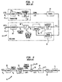
- FIG 1 A baseband communication system is shown in FIG 1 (see Lee et at, page 148).
- the baseband system 10 of FIG 1 includes a transmitter 12 and a receiver 14. At the transmitter 12, an incoming stream of bits B k is coded by a coder 16 into a stream of symbols A k .
- the alphabet is the set of symbols that are available for transmission.
- a baseband signal has a real-valued alphabet that is simply a list of real numbers, for example A k assumes values from the alphabet ⁇ -3, -1, +1, +3 ⁇ .
- the coder 16 in the baseband transmitter 12 can, for example, map pairs of bits from the set ⁇ 00, 01, 10, 11 ⁇ into one of four levels from the alphabet ⁇ -3, -1, 1, 3 ⁇ .
- the coder 16 may map multiple bits into a single data symbol, there is a distinction between the “symbol rate” and the “bit rate”.
- the “symbol rate” is also called the "baud rate”. If for example, the coder maps two bits into each symbol, the symbol rate is one-half of the bit rate.
- the symbols A k are applied to a transmit filter 18.
- the transmit filter 18 produces a continuous-time signal s(t) for transmission over the continuous time channel 20.
- the impulse response g(t) of the transmit filter 18 is called the pulse shape.
- PAM pulse amplitude modulated
- Baseband PAM and its generalization to passband are among the most common signaling methods.
- a variety of techniques including QAM, PSK, BPSK, PRK, QPSK, DPSK and AM-PM are special cases of PAM. See Lee et al, pages 149-150.
- the signal R(t) which is received via the channel 20 is processed by a receiver filter 21 with an impulse response f(t) to produce the output signal Q(t).
- the received signal R(t) is also processed by a timing recovery circuit 22 which recovers a clock for use by the sampler 24.
- the signal Q(t) is sampled by the sampler circuit 24.
- the samples Q k outputted by the sampler 24 are processed by a decision device 26 to form the reconstructed symbols ⁇ k .
- the symbols are decoded by a decoder 28 to form the reconstructed bit stream B ⁇ k .
- the passband strategy is now considered.
- the passband strategy is considered using a discrete time signal representation.
- the passband strategy is to construct a signal s(nT) where s(nT) is the discrete time analog to s(t) and where 1/T is the sampling rate.
- the signal s(nT) is in this case complex and contains information in both its real and imaginary parts.
- the signal s(nT) is modulated using a complex-valued carrier to obtain a modulated signal z(nT).
- a transmitter 30 for accomplishing this is schematically illustrated in FIG 2 (see Lee et al, page 170).
- a complex-valued alphabet is best described by plotting the alphabet as a set of points in a complex plane. Such a plot is called a signal constellation. Two popular constellations are illustrated in FI 3A and FIG 3B.
- the complex symbols 2a(kT) are processed by the transmit filter 34.
- the transmit filter 34 of FIG 2 has a transfer function h(nT).
- the output of the transmit filter 34 is the complex baseband signal
- the signal z(nT) is complex valued, so that it cannot be transmitted over a real-valued channel. However, all of the signal information is contained in the real part of the signal, which can be transmitted over a real-valued channel.
- the ⁇ 2 ⁇ factor insures that the power of x(nT) is the same as the power in s(nT).
- Timing in the discrete-time transmitter 30 of FIG 2 is controlled by a transmitter clock (not shown).
- the signal x(nT) is processed by the digital-to-analog converter 40 to convert to a continuous-time signal x(t) for transmission to a remote receiver via a transmission channel 41.
- the function z(nT) is analytic, i.e., its Fourier transform contains no negative frequency components.
- FIG 4 shows an alternative embodiment for the transmitter shown in FIG 2 (see Lee et al, page 172).
- bit stream b k is processed by a coder 51 to form the real symbol streams Re ⁇ a k ⁇ and Im ⁇ a k ⁇ .
- Each symbol stream is processed by a transmit filter 52 with a transfer function ⁇ 2 ⁇ h(nT) to form the first and second baseband signals s r (nT) and s i (nT).
- the first baseband signal is then multiplied by the carrier cos( ⁇ c nT) in the modulator 53 and the second baseband signal is multiplied by the carrier sin ⁇ c nT in the modulator 54.
- the signals are then combined using the subtractor element 55 to form the passband signal x(nT). This signal is converted to the analog signal x(t) by the digital-to-analog converter 56.
- the bit rate may be 9600 bits/sec or 4800 bits/sec.
- a receiver for receiving a continuous-time pulse amplitude modulated (PAM) passband signal comprises an analog-to-digital converter for sampling the continuous-time PAM passband signal using a local clock to generate received samples.
- the received samples are then corrected for any asynchronism between the local receiver clock and a remote transmitter clock.
- the timing utilized at the transmitter is locally recovered at the receiver.
- a timing adjustment filter evaluates a convolution of the received samples obtained using the local clock and an impulse response function at a particular value of a phase difference variable.
- the timing adjustment filter outputs corrected samples.
- a corrected sample is an optimum sample when the corrected sample is obtained at the optimum value of the phase difference variable. At the optimum value of the phase difference variable, there is synchronization between the local and remote clocks.
- phase difference variable used to evaluate the convolution is obtained using a feedback technique as follows.
- a periodic signal is derived from the corrected samples generated by the timing adjustment filter. This signal is illustratively a sinusoidal signal at the symbol rate.
- a timing difference detector compares, during each period of the periodic signal, successive samples of the periodic signal, to determine whether the corrected samples are ahead of or lag behind the optimal samples.
- the phase difference variable is increased or decreased by a fixed discrete stepsize in each period of the periodic signal until the optimum value of the phase difference variable is reached and the corrected samples are optimum samples. In this manner, synchronization between the local and remote clocks is achieved.
- FIG 1 schematically illustrates a baseband PAM system.
- FIG 2 illustrates a PAM passband transmitter
- FIGs 3A and FIB 3B illustrate symbol alphabets utilized in passband PAM.
- FIG 4 illustrates an alternative PAM passband transmitter.
- FIG 5 and FIG 6 illustrate a PAM passband receiver in accordance with an illustrative embodiment of the present invention.
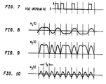
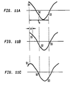
- FIGs 7, 8, 9,10, 11(a), 11(b) and 11(c) illustrate certain signals utilized in the receiver of FIG 5.
- a receiver 60 in accordance with the present invention is illustrated in FIG 5.
- the continuous-time signal x(t) which is generated by the transmitter (see FIG 3 and FIG 5) and transmitted by a channel 59 with a particular transfer characteristic, is received at the receiver 60 of FIG 5 as the continuous-time signal y(t).
- the samples y(nT) are then processed by a timing adjuster 62 which generates the corrected samples y' n .
- B is 3000 Hz.
- N is a finite integer.
- the parameter a is known as the roll-off factor and is illustratively equal to 0.1.
- the variable v is a time variable equal to nT+ ⁇ in equation 8.
- the corrected sample y' n is an optimum sample.
- the value of the phase difference variable ⁇ is determined by the timing difference detector 70.
- the timing difference detector 70 adjusts the value of ⁇ until the optimum value ⁇ 0 is reached. The operation of the timing difference detector 70 is discussed below.
- the corrected samples y' n are processed by the passband PAM receiver 64.
- the operation of the passband PAM receiver 64 is shown in greater detail in FIG 6.
- the impulse response is complex, two real filters with impulse responses Re ⁇ h(mT) ⁇ and Im ⁇ H(mT) ⁇ are required for the implementation.
- the receiver filter 80 passes no negative frequencies. This means that the output signal contains no negative frequency components.
- the filter f(mT) is a simple low pass fitter with unity gain in the passband.
- a symbol synchronization technique is used to choose a value of the phase difference variable ⁇ .
- FIG 7 shows a waveform with a unipolar RZ format (in a continuous-time representation).
- the power spectrum density of this signal has a delta function at the symbol rate. Consequently, the symbol clock signal can be obtained by passing the unipolar RZ waveform through a narrow-band pass filter that is tuned to the symbol rate.
- the output of the passband PAM receiver 64 of FIG 5 does not have a unipolar RZ format. In this case it is necessary to convert the output of the passband PAM receiver 64 into the unipolar RZ waveform.
- the output of the passband PAM receiver 64 might have a polar NRZ format.
- the polar NRZ format is shown in FIG 8 in a continuous-time representation.
- a square-law circuit may be used to convert the output of the passband PAM receiver into the RZ unipolar format.
- a square law circuit 66 computes r r 2(mT)+r i 2(mT).
- the output of the square law circuit 66 is shown in FIG 9 (in a continuous time representation for purposes of clarify).
- a narrow bandpass filter 68 that is tuned to the symbol frequency filters the output signal of the square law circuit 66.
- FIG 10 See Leon W. Couch II, "Digital Analog Communication Systems", Third Edition, 1990, McMillan Publishing Co., New York, page 157).
- the timing difference detector 70 of FIG 5 receives the clock signal outputted by the narrow bandpass filter 68 and determines a value for ⁇ to be used in the timing adjuster 62 for evaluating the convolution of equation (8). More particularly, the values of the phase difference variable ⁇ are chosen by the timing difference detector 70 for evaluating the convolution of equation 8 to obtain y' n so as to cause the corrected samples y' n to more closely approach the optimum samples. It should be noted that when the corrected samples are optimum samples, ⁇ constant. When this circumstance prevails, it means the local and remote clocks are synchronous.
- the corrected samples y' n are called optimum samples when the phase difference variable ⁇ has the optimum value ⁇ 0.
- a symbol sample r(mT) obtained at the output of the PAM receiver 64 of FIG 5 at the optimum sampling time (e.g., which results in a symbol clock signal with positive peaks at 2400 Hz) is easily processed to identify which symbol from the alphabet is transmitted at the transmitter.
- FIG 11(a) shows the symbol clock signal when the corrected samples are optimum samples
- FIG 11(b) shows the symbol clock when the corrected samples lag behind the optimum samples
- FIG 11(c) shows the symbol clock when the corrected samples lead the optimum samples.
- timing difference detector 70 The operation of the timing difference detector 70 is now considered.
- the local receiver clock is said to be synchronous to the transmitter clock if the local receiver clock has a precise frequency and phase relationship with respect to the received input signal, and it is delayed when compared to the clock at the transmitter since there is a propagation delay through the channel. In other words, the local receiver clock is synchronized to the input symbol stream at the transmitter.
- the symbol clock signal will be that of FIG 11(a) where S2 ⁇ S3.
- the phase difference ⁇ approximates a constant and the ⁇ value is approximately zero.
- this technique of adjusting ⁇ does not indicate whether the local receiver clock is too slow or too fast relative to the remote clock. However, in general, when the local clock is slower than the remote clock, it is more likely that S3>S2 than S3 ⁇ S2. When the local clock is faster than the remote clock, it is more likely that S3 ⁇ S2 than S3>S2.
- the asynchronization problem as described above will result in one sample of the received signal being lost if the local clock is too slow or in an extra sample of the received signal being obtained if the local clock is too fast.
- ⁇ is smaller than a predetermined limit, such as if ⁇ -0.875, it means that the local receiver clock is slower than the remote transmitter clock and one corrected sample (i.e., the input to the subsequent passband PAM receiver) will be lost.
- a predetermined limit such as if ⁇ -0.875
- the phase difference variable used to evaluate equation (8) is changed to ⁇ +1.0.
- the new phase difference variable ⁇ is used to evaluate the convolution of equation 8 to generate an additional corrected sample.
- ⁇ is larger than a predetermined limit, such as ⁇ >0.875, it means that the local receiver is faster than the remote transmitter clock and one extra corrected sample data will be obtained. To correct this, the next received sample is processed by the timing adjuster, and the corrected sample generated by the convolution of equation (8) is discarded. Second, the phased difference variable used to evaluate equation (8) is changed to ⁇ -1.0.
- the inventive receiver of FIG 5 has been viewed as comprising a plurality of interconnected circuit elements. While this is one approach to implementing the inventive receiver, in another approach the receiver may be implemented through use of a single digital signal processor or microprocessor which implements the functions shown in FIG 5 under software control.
Landscapes
- Engineering & Computer Science (AREA)
- Computer Networks & Wireless Communication (AREA)
- Signal Processing (AREA)
- Digital Transmission Methods That Use Modulated Carrier Waves (AREA)
- Electric Clocks (AREA)
- Synchronisation In Digital Transmission Systems (AREA)
Applications Claiming Priority (2)
| Application Number | Priority Date | Filing Date | Title |
|---|---|---|---|
| US894030 | 1992-06-05 | ||
| US07/894,030 US5404379A (en) | 1991-01-28 | 1992-06-05 | Timing recovery method and system |
Publications (2)
| Publication Number | Publication Date |
|---|---|
| EP0573696A1 true EP0573696A1 (de) | 1993-12-15 |
| EP0573696B1 EP0573696B1 (de) | 2003-03-19 |
Family
ID=25402500
Family Applications (1)
| Application Number | Title | Priority Date | Filing Date |
|---|---|---|---|
| EP92117163A Expired - Lifetime EP0573696B1 (de) | 1992-06-05 | 1992-10-08 | Taktwiedergewinnungsverfahren und -system |
Country Status (4)
| Country | Link |
|---|---|
| US (1) | US5404379A (de) |
| EP (1) | EP0573696B1 (de) |
| AT (1) | ATE235126T1 (de) |
| DE (1) | DE69232966T2 (de) |
Cited By (3)
| Publication number | Priority date | Publication date | Assignee | Title |
|---|---|---|---|---|
| WO1998001974A1 (fr) * | 1996-07-10 | 1998-01-15 | Compagnie Des Signaux | Recuperation d'horloge pour recepteur d'un systeme de transmission synchrone |
| US5917856A (en) * | 1994-10-31 | 1999-06-29 | Nokia Telecommunications Oy | Method for establishing a PAM signal connection using a training sequence |
| WO2007126957A2 (en) | 2006-03-31 | 2007-11-08 | Novartis Ag | New compounds |
Families Citing this family (12)
| Publication number | Priority date | Publication date | Assignee | Title |
|---|---|---|---|---|
| DE69534154T2 (de) * | 1994-06-10 | 2005-09-22 | Ntt Docomo, Inc. | Empfänger |
| JP4089984B2 (ja) * | 1994-08-31 | 2008-05-28 | ローム株式会社 | サンプルホールド回路 |
| DE19516449B4 (de) * | 1995-05-04 | 2011-04-28 | Palm, Inc. (n.d.Ges. d. Staates Delaware), Sunnyvale | Verfahren zum Bestimmen der Frequenzabweichung |
| US6167241A (en) * | 1996-10-28 | 2000-12-26 | Int Labs, Inc. | Technique for performing amplitude modulation without cheating side-bands |
| AU9805498A (en) | 1997-10-16 | 1999-05-03 | Int Labs, Inc. | Data transfer over wire or wireless medium |
| KR100585489B1 (ko) * | 1997-12-17 | 2006-08-23 | 엘지노텔 주식회사 | 타이밍검출장치 |
| US20030224704A1 (en) * | 2002-05-28 | 2003-12-04 | James Shank | Rotary media valve |
| TWI235575B (en) * | 2003-06-13 | 2005-07-01 | Realtek Semiconductor Corp | Sampling error phase compensator and method thereof |
| JP5540224B2 (ja) * | 2009-07-17 | 2014-07-02 | エタニ電機株式会社 | インパルス応答測定方法およびインパルス応答測定装置 |
| JP5590934B2 (ja) * | 2010-03-24 | 2014-09-17 | スパンション エルエルシー | スイッチング電源の制御回路及び電子機器 |
| CN110521127B (zh) * | 2018-12-12 | 2021-07-27 | 深圳市汇顶科技股份有限公司 | 用于射频收发器中峰值自适应采样解调的系统和方法 |
| US10742222B2 (en) * | 2018-12-12 | 2020-08-11 | Shenzhen GOODIX Technology Co., Ltd. | Peak-adaptive sampling demodulation for radiofrequency transceivers |
Citations (3)
| Publication number | Priority date | Publication date | Assignee | Title |
|---|---|---|---|---|
| EP0092400A2 (de) * | 1982-04-20 | 1983-10-26 | Trw Inc. | Digitales Synchronisationsverfahren |
| EP0173569A2 (de) * | 1984-08-29 | 1986-03-05 | Fujitsu Limited | Empfängereinheit mit Synchronisierungseinlaufschaltung |
| EP0222593A2 (de) * | 1985-11-05 | 1987-05-20 | Signal Processors Limited | Digitale Filter und Demodulatoren |
Family Cites Families (11)
| Publication number | Priority date | Publication date | Assignee | Title |
|---|---|---|---|---|
| JPS5152264A (de) * | 1974-09-11 | 1976-05-08 | Sharp Kk | |
| AU554851B2 (en) * | 1984-09-19 | 1986-09-04 | Siemens Aktiengesellschaft | Digital transmission system |
| CA1268523A (en) * | 1984-10-31 | 1990-05-01 | Nec Corporation | Synchronization circuit capable of establishing synchronism even when a sampling rate is invariable |
| US4731800A (en) * | 1986-10-03 | 1988-03-15 | Hycom Incorporated | Raised-cosine filtering for modems |
| US4755795A (en) * | 1986-10-31 | 1988-07-05 | Hewlett-Packard Company | Adaptive sample rate based on input signal bandwidth |
| JP2548210B2 (ja) * | 1987-07-21 | 1996-10-30 | 松下電器産業株式会社 | 時間軸補正装置 |
| US4815103A (en) * | 1987-10-29 | 1989-03-21 | American Telephone And Telegraph Company | Equalizer-based timing recovery |
| US4866739A (en) * | 1988-02-22 | 1989-09-12 | Silicon Systems, Inc. | Digital fast recovery timing algorithm |
| US4847864A (en) * | 1988-06-22 | 1989-07-11 | American Telephone And Telegraph Company | Phase jitter compensation arrangement using an adaptive IIR filter |
| US5018166A (en) * | 1989-10-10 | 1991-05-21 | Hayes Microcomputer Products, Inc. | Method and apparatus for baud timing recovery |
| US5309482A (en) * | 1992-03-30 | 1994-05-03 | Novatel Communications Ltd. | Receiver having an adjustable matched filter |
-
1992
- 1992-06-05 US US07/894,030 patent/US5404379A/en not_active Expired - Fee Related
- 1992-10-08 DE DE69232966T patent/DE69232966T2/de not_active Expired - Lifetime
- 1992-10-08 EP EP92117163A patent/EP0573696B1/de not_active Expired - Lifetime
- 1992-10-08 AT AT92117163T patent/ATE235126T1/de not_active IP Right Cessation
Patent Citations (3)
| Publication number | Priority date | Publication date | Assignee | Title |
|---|---|---|---|---|
| EP0092400A2 (de) * | 1982-04-20 | 1983-10-26 | Trw Inc. | Digitales Synchronisationsverfahren |
| EP0173569A2 (de) * | 1984-08-29 | 1986-03-05 | Fujitsu Limited | Empfängereinheit mit Synchronisierungseinlaufschaltung |
| EP0222593A2 (de) * | 1985-11-05 | 1987-05-20 | Signal Processors Limited | Digitale Filter und Demodulatoren |
Non-Patent Citations (1)
| Title |
|---|
| PROCEEDINGS IEEE GLOBAL TELECOMMUNICATIONS CONFERENCE vol. 1, 2 December 1990, SAN DIEGO (US) pages 589 - 593 MARTIN OERDER ET AL. 'VLSI implementation of synchronization algorithms in a 100 Mbit/s digital receiver' * |
Cited By (11)
| Publication number | Priority date | Publication date | Assignee | Title |
|---|---|---|---|---|
| US5917856A (en) * | 1994-10-31 | 1999-06-29 | Nokia Telecommunications Oy | Method for establishing a PAM signal connection using a training sequence |
| WO1998001974A1 (fr) * | 1996-07-10 | 1998-01-15 | Compagnie Des Signaux | Recuperation d'horloge pour recepteur d'un systeme de transmission synchrone |
| FR2751152A1 (fr) * | 1996-07-10 | 1998-01-16 | Philips Electronics Nv | Recuperation d'horloge pour recepteur d'un systeme de transmission synchrone |
| WO2007126957A2 (en) | 2006-03-31 | 2007-11-08 | Novartis Ag | New compounds |
| EP2301923A1 (de) | 2006-03-31 | 2011-03-30 | Novartis AG | Neue Verbindungen |
| EP2402319A1 (de) | 2006-03-31 | 2012-01-04 | Novartis AG | DGAT Inhibitoren |
| EP2402320A1 (de) | 2006-03-31 | 2012-01-04 | Novartis AG | Anorektische Agenten |
| EP2402318A1 (de) | 2006-03-31 | 2012-01-04 | Novartis AG | DGAT Inhibitoren |
| EP2402317A1 (de) | 2006-03-31 | 2012-01-04 | Novartis AG | DGAT Inhibitor |
| EP2404905A1 (de) | 2006-03-31 | 2012-01-11 | Novartis AG | Neue Verbindungen |
| EP2418202A1 (de) | 2006-03-31 | 2012-02-15 | Novartis AG | Neue Verbindungen |
Also Published As
| Publication number | Publication date |
|---|---|
| DE69232966D1 (de) | 2003-04-24 |
| EP0573696B1 (de) | 2003-03-19 |
| US5404379A (en) | 1995-04-04 |
| ATE235126T1 (de) | 2003-04-15 |
| DE69232966T2 (de) | 2003-10-09 |
Similar Documents
| Publication | Publication Date | Title |
|---|---|---|
| US6055281A (en) | Passband DQPSK detector for a digital communications receiver | |
| US4229821A (en) | System for data transmission by means of an angle-modulated carrier of constant amplitude | |
| Anderson et al. | Digital phase modulation | |
| EP0748118B1 (de) | Signalverarbeitungssystem | |
| EP0610683B1 (de) | Digitale Taktrückgewinnungsschaltung | |
| US5404379A (en) | Timing recovery method and system | |
| US6606010B1 (en) | Quadrature vestigial sideband digital communications method | |
| US5425058A (en) | MSK phase acquisition and tracking method | |
| US5048058A (en) | MSK modulation and differentially coherent detection transmission system | |
| US5802461A (en) | Apparatus and method for timing recovery in vestigial sibeband modulation | |
| WO2001020863A9 (en) | Method and apparatus for carrier phase tracking | |
| US5793821A (en) | Timing Recovery using group delay compensation | |
| US6148040A (en) | Precoded gaussian minimum shift keying carrier tracking loop | |
| GB2232852A (en) | Offset correction | |
| US4603393A (en) | Demodulator for constant envelope and continuous phase signals which are angle modulated by a train of binary symbols | |
| Galko et al. | Linear receivers for correlatively coded MSK | |
| US6996191B1 (en) | Efficient accurate controller for envelope feedforward power amplifiers | |
| KR100281430B1 (ko) | 가변속도 비동기 모뎀 | |
| KR100542091B1 (ko) | 무반송파 진폭 위상(cap) 신호용 부호 타이밍 복구 네트워크 | |
| JP3517056B2 (ja) | Vsb変調信号におけるサンプリングタイミング位相誤差検出器 | |
| US6771713B1 (en) | Data aided carrier phase tracking system for precoded continuous phase modulated signals | |
| KR880001166B1 (ko) | 데이타 모뎀 클록 추출회로 | |
| US20090016467A1 (en) | Noncoherent symbol clock recovery subsystem | |
| EP0244057B1 (de) | Kommunikationssystem, Empfänger und Sender und Methode zur Datenrückgewinnung | |
| JPH084277B2 (ja) | デジタル通信システム |
Legal Events
| Date | Code | Title | Description |
|---|---|---|---|
| PUAI | Public reference made under article 153(3) epc to a published international application that has entered the european phase |
Free format text: ORIGINAL CODE: 0009012 |
|
| AK | Designated contracting states |
Kind code of ref document: A1 Designated state(s): AT BE DE FR GB |
|
| 17P | Request for examination filed |
Effective date: 19931120 |
|
| 17Q | First examination report despatched |
Effective date: 19991019 |
|
| GRAH | Despatch of communication of intention to grant a patent |
Free format text: ORIGINAL CODE: EPIDOS IGRA |
|
| GRAH | Despatch of communication of intention to grant a patent |
Free format text: ORIGINAL CODE: EPIDOS IGRA |
|
| GRAA | (expected) grant |
Free format text: ORIGINAL CODE: 0009210 |
|
| AK | Designated contracting states |
Designated state(s): AT BE DE FR GB |
|
| REG | Reference to a national code |
Ref country code: GB Ref legal event code: FG4D |
|
| REF | Corresponds to: |
Ref document number: 69232966 Country of ref document: DE Date of ref document: 20030424 Kind code of ref document: P |
|
| ET | Fr: translation filed | ||
| PGFP | Annual fee paid to national office [announced via postgrant information from national office to epo] |
Ref country code: FR Payment date: 20031016 Year of fee payment: 12 |
|
| PGFP | Annual fee paid to national office [announced via postgrant information from national office to epo] |
Ref country code: AT Payment date: 20031027 Year of fee payment: 12 |
|
| PLBE | No opposition filed within time limit |
Free format text: ORIGINAL CODE: 0009261 |
|
| STAA | Information on the status of an ep patent application or granted ep patent |
Free format text: STATUS: NO OPPOSITION FILED WITHIN TIME LIMIT |
|
| 26N | No opposition filed |
Effective date: 20031222 |
|
| PGFP | Annual fee paid to national office [announced via postgrant information from national office to epo] |
Ref country code: BE Payment date: 20040827 Year of fee payment: 13 |
|
| PG25 | Lapsed in a contracting state [announced via postgrant information from national office to epo] |
Ref country code: AT Free format text: LAPSE BECAUSE OF NON-PAYMENT OF DUE FEES Effective date: 20041008 |
|
| PG25 | Lapsed in a contracting state [announced via postgrant information from national office to epo] |
Ref country code: FR Free format text: LAPSE BECAUSE OF NON-PAYMENT OF DUE FEES Effective date: 20050630 |
|
| REG | Reference to a national code |
Ref country code: FR Ref legal event code: ST |
|
| PG25 | Lapsed in a contracting state [announced via postgrant information from national office to epo] |
Ref country code: BE Free format text: LAPSE BECAUSE OF NON-PAYMENT OF DUE FEES Effective date: 20051031 |
|
| BERE | Be: lapsed |
Owner name: *INDUSTRIAL TECHNOLOGY RESEARCH INSTITUTE Effective date: 20051031 |
|
| PGFP | Annual fee paid to national office [announced via postgrant information from national office to epo] |
Ref country code: DE Payment date: 20101027 Year of fee payment: 19 |
|
| PGFP | Annual fee paid to national office [announced via postgrant information from national office to epo] |
Ref country code: GB Payment date: 20101025 Year of fee payment: 19 |
|
| REG | Reference to a national code |
Ref country code: DE Ref legal event code: R071 Ref document number: 69232966 Country of ref document: DE |
|
| REG | Reference to a national code |
Ref country code: DE Ref legal event code: R071 Ref document number: 69232966 Country of ref document: DE |
|
| REG | Reference to a national code |
Ref country code: GB Ref legal event code: PE20 Expiry date: 20121007 |
|
| PG25 | Lapsed in a contracting state [announced via postgrant information from national office to epo] |
Ref country code: GB Free format text: LAPSE BECAUSE OF EXPIRATION OF PROTECTION Effective date: 20121007 |