EP0570664A2 - Circuit pour l'alimentation d'impulsions de toxation sur une ligne de connexion pour un terminal de télécommunication - Google Patents
Circuit pour l'alimentation d'impulsions de toxation sur une ligne de connexion pour un terminal de télécommunication Download PDFInfo
- Publication number
- EP0570664A2 EP0570664A2 EP93101541A EP93101541A EP0570664A2 EP 0570664 A2 EP0570664 A2 EP 0570664A2 EP 93101541 A EP93101541 A EP 93101541A EP 93101541 A EP93101541 A EP 93101541A EP 0570664 A2 EP0570664 A2 EP 0570664A2
- Authority
- EP
- European Patent Office
- Prior art keywords
- low
- pass filter
- pulse
- circuit arrangement
- frequency
- Prior art date
- Legal status (The legal status is an assumption and is not a legal conclusion. Google has not performed a legal analysis and makes no representation as to the accuracy of the status listed.)
- Withdrawn
Links
Images

Classifications
-
- H—ELECTRICITY
- H04—ELECTRIC COMMUNICATION TECHNIQUE
- H04M—TELEPHONIC COMMUNICATION
- H04M15/00—Arrangements for metering, time-control or time indication ; Metering, charging or billing arrangements for voice wireline or wireless communications, e.g. VoIP
Definitions
- the invention relates to a circuit arrangement for feeding charge pulses on a connecting line for a telecommunication terminal according to the preamble of claim 1.
- a circuit arrangement for the low-noise feeding of pulses from a sinusoidal AC voltage, in particular 16 kHz charge pulses, is known from European Patent Specification 0 206 279.
- a MOS-FET switch is provided, the control input of which is connected to an RC parallel element. This switch connects a central AC voltage source to a winding of a line transformer each time a charge pulse is to be fed in.
- a so-called soft keying of the switch is achieved, i.e. the rise and fall times of the pulse edges are slowed down by charging and discharging the capacitor accordingly slowly. This is to avoid noise disturbances that could result when pulses are fed in.
- the object of the invention is to provide a circuit arrangement with which charge pulses can be switched on connecting lines for telecommunication devices without inductors or winding goods being required.
- the circuit arrangement should be designed so that its components can be summarized in integrated circuits.
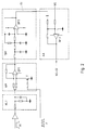
- An activation pulse AI which occurs whenever a charge pulse GI is to be fed in, is fed to the input of an RC low-pass filter RCT.
- this RC low-pass filter RCT consists of a series connection of a resistor with a capacitor.
- an envelope curve HK appears, which no longer has the rectangular shape of the activation pulse AI but gradually increases and decreases following an e-function.
- the input of an amplitude modulator AM is connected to the output of the RC low-pass filter RCT.
- Another input of the amplitude modulator AM is connected to a generator G, which generates the frequency F of the charge pulse. This frequency F appears at the output of the amplitude modulator AM with an amplitude predetermined by the envelope curve HK.
- the output of the amplitude modulator AM is connected to a low-pass filter TPF, which has the task of smoothing the steep edges of the signal supplied by the amplitude modulator AM.
- a charge pulse GI thus takes the form of an increasing and decaying sine wave at the output of the low-pass filter TPF. Since the output of the low-pass filter TPF is connected to an input of an analog adder AA which receives the analog low-frequency useful signal NS at its other input, a signal is generated within the analog adder AA in which the charge pulse GI corresponds to the analog low-frequency useful signal NS is superimposed. This signal NS + GI reaches the connecting line AL to a terminal EG connected to it. This type of feeding a charge pulse GI ensures that no transmission disturbances occur. This also applies if, for example, a facsimile machine or another digital device is in operation instead of a telephone set.
- the circuit diagram shown in FIG. 2 indicates how the individual parts of the entire circuit arrangement are connected to one another.
- the drive pulse AI is deformed by the time constant of the capacitor in the RC low-pass filter RCT, as shown in the drawing in FIG.
- This pulse is connected to the inputs of an operational amplifier OP1, which is operated as a switchable differential amplifier (gain factor + 1 / -1), the frequency F of the charge pulse being switched to one of the inputs via a transistor T.
- an operational amplifier OP1 which is operated as a switchable differential amplifier (gain factor + 1 / -1)
- the frequency F of the charge pulse being switched to one of the inputs via a transistor T.
- This signal is fed to a low-pass filter TPF, which consists of an operational amplifier OP2, which is connected to resistors and capacitors at its inputs and outputs.
- TPF low-pass filter
- the signal of the charge pulse GI which arises at the output of the operational amplifier OP2 in the active low-pass filter TPF is now fed to the analog adder AA.
- This analog adder AA consists of an operational amplifier OP3 at whose one input the useful signal NS and the charge pulse GI shaped as described above are interconnected. This produces an output signal at the output of the operational amplifier OP3, the charge pulse GI being superimposed on the useful signal NS. This signal is then sent via the connecting line AL to a terminal EG.
Landscapes
- Engineering & Computer Science (AREA)
- Computer Networks & Wireless Communication (AREA)
- Signal Processing (AREA)
- Interface Circuits In Exchanges (AREA)
- Meter Arrangements (AREA)
- Amplifiers (AREA)
Applications Claiming Priority (2)
| Application Number | Priority Date | Filing Date | Title |
|---|---|---|---|
| DE4216577 | 1992-05-20 | ||
| DE19924216577 DE4216577C1 (fr) | 1992-05-20 | 1992-05-20 |
Publications (2)
| Publication Number | Publication Date |
|---|---|
| EP0570664A2 true EP0570664A2 (fr) | 1993-11-24 |
| EP0570664A3 EP0570664A3 (en) | 1994-07-06 |
Family
ID=6459269
Family Applications (1)
| Application Number | Title | Priority Date | Filing Date |
|---|---|---|---|
| EP19930101541 Withdrawn EP0570664A3 (en) | 1992-05-20 | 1993-02-02 | Circuit arrangement for feeding metering pulses to a connection line for a telecommunications terminal apparatus |
Country Status (4)
| Country | Link |
|---|---|
| EP (1) | EP0570664A3 (fr) |
| DE (1) | DE4216577C1 (fr) |
| FI (1) | FI932294A (fr) |
| NO (1) | NO930424L (fr) |
Families Citing this family (2)
| Publication number | Priority date | Publication date | Assignee | Title |
|---|---|---|---|---|
| DE4408323C2 (de) * | 1994-03-11 | 1999-03-11 | Siemens Ag | Verfahren zur Erzeugung eines digitalen Sinussignales mit einer vorgegebenen Abtastrate und Schaltungsanordnung zur Durchführung des Verfahrens |
| DE10146891C2 (de) * | 2001-09-24 | 2003-08-14 | Infineon Technologies Ag | Verfahren zum Übertragen von Gebührenbestimmungssignalen über einen Datenübertragungspfad und Vorrichtung zur Spannungspegelgenerierung |
Citations (2)
| Publication number | Priority date | Publication date | Assignee | Title |
|---|---|---|---|---|
| EP0145038A2 (fr) * | 1983-09-19 | 1985-06-19 | BELL TELEPHONE MANUFACTURING COMPANY Naamloze Vennootschap | Circuits électroniques et générateur de signal utilisant ces circuits |
| JPH0422263A (ja) * | 1990-05-17 | 1992-01-27 | Fujitsu Ltd | 課金信号作成回路 |
Family Cites Families (2)
| Publication number | Priority date | Publication date | Assignee | Title |
|---|---|---|---|---|
| DE3237550C1 (de) * | 1982-10-09 | 1983-09-29 | Standard Elektrik Lorenz Ag, 7000 Stuttgart | Schaltungsanordnung zum geräuscharmen Ein- und Ausschalten von Impulsen aus einer sinusförmigen Wechselspannung, insbesondere von 16 kHz-Zählimpulsen in Fernsprechanlagen |
| PT82786B (pt) * | 1985-06-21 | 1992-07-31 | Siemens Ag | Circuito para a injeccao com pouco ruido de impulsos de uma tensao alternada sinusoidal em especial de impulsos de taxacao de 16 khz |
-
1992
- 1992-05-20 DE DE19924216577 patent/DE4216577C1/de not_active Expired - Fee Related
-
1993
- 1993-02-02 EP EP19930101541 patent/EP0570664A3/de not_active Withdrawn
- 1993-02-08 NO NO930424A patent/NO930424L/no unknown
- 1993-05-19 FI FI932294A patent/FI932294A/fi not_active Application Discontinuation
Patent Citations (2)
| Publication number | Priority date | Publication date | Assignee | Title |
|---|---|---|---|---|
| EP0145038A2 (fr) * | 1983-09-19 | 1985-06-19 | BELL TELEPHONE MANUFACTURING COMPANY Naamloze Vennootschap | Circuits électroniques et générateur de signal utilisant ces circuits |
| JPH0422263A (ja) * | 1990-05-17 | 1992-01-27 | Fujitsu Ltd | 課金信号作成回路 |
Non-Patent Citations (1)
| Title |
|---|
| PATENT ABSTRACTS OF JAPAN Bd. 16, Nr. 185 (E-1197) 06 Mai 1992 & JP-A-04 022 263 (FUJITSU LTD) 27 Januar 1992 * |
Also Published As
| Publication number | Publication date |
|---|---|
| NO930424D0 (no) | 1993-02-08 |
| EP0570664A3 (en) | 1994-07-06 |
| FI932294A (fi) | 1993-11-21 |
| DE4216577C1 (fr) | 1993-05-06 |
| FI932294A0 (fi) | 1993-05-19 |
| NO930424L (no) | 1993-11-22 |
Similar Documents
| Publication | Publication Date | Title |
|---|---|---|
| DE3221693A1 (de) | Teilnehmeranschlussschaltung fuer fernsprechanlagen | |
| DE2806852A1 (de) | Verstaerkereinrichtung | |
| DE1237615B (de) | Schaltungsanordnung zur Erzeugung der Tast-frequenz fuer frequenzmodulierte Telegrafiezeichen | |
| DE2040436A1 (de) | Phasenkohaerenter und amplitudenstabiler Frequenzverschiebungsoszillator | |
| DE2524072C2 (de) | Leistungsverstärker für in der Impulsbreite modulierte Signale | |
| DE1245418B (de) | Ohne Bezugswert arbeitender Impulsphasen-Demodulator | |
| DE2456344C3 (de) | Tonfrequenz-Rundsteueranlage | |
| DE2917916C3 (de) | Pulsdauermodulations-Signalverstärker | |
| DE3604404A1 (de) | Rauschunterdrueckungssignalkompensations- schaltung | |
| DE2807916C3 (de) | Wecksignalgenerator zur Verwendung in einer Teilnehmerverbindungsschaltung | |
| DE2411871C2 (de) | Schaltungsanordnung zur erdfreien Übertragung von Signalen über Trennstellen in Fernmeldeanlagen | |
| EP0570664A2 (fr) | Circuit pour l'alimentation d'impulsions de toxation sur une ligne de connexion pour un terminal de télécommunication | |
| EP0171470B1 (fr) | Dispositif d'alimentation d'émetteurs et de récepteurs d'un système de transmission de signaux | |
| DE2903860A1 (de) | Einrichtung zur gleichstromversorgung eines verbrauchers und zur gleichzeitigen informationsuebertragung ueber ein aderpaar | |
| DE3303133C2 (fr) | ||
| DE3530299A1 (de) | Schaltungsanordnung zur reduzierung des kantenrauschens bei der uebertragung von videosignalen | |
| EP0499869B1 (fr) | Circuit pour génération de tension alternative | |
| EP0477660B1 (fr) | Circuit de reception d'informations transmises sur les lignes de puissance | |
| DE1962197A1 (de) | Datenuebertragungsanlage | |
| DE2736522C2 (de) | Schaltungsanordnung zum Obertragen von Daten | |
| DE3611226C2 (fr) | ||
| DE2734303C3 (de) | Regenerator für ein pulsförmiges periodisches Taktsignal | |
| DE2735498A1 (de) | Schaltungsanordnung mit einem induktiven wandler | |
| EP0519088B1 (fr) | Méthode et circuit pour limitation d'un signal de sortie | |
| DE1940903C2 (de) | Verfahren zur Erzeugung und Absiebung von Oberwellen einer Grundfrequenz, insbesondere von Frequenzen für Trägerfrequenzsysteme |
Legal Events
| Date | Code | Title | Description |
|---|---|---|---|
| PUAI | Public reference made under article 153(3) epc to a published international application that has entered the european phase |
Free format text: ORIGINAL CODE: 0009012 |
|
| AK | Designated contracting states |
Kind code of ref document: A2 Designated state(s): AT BE CH DE ES FR GB GR IT LI NL SE |
|
| PUAL | Search report despatched |
Free format text: ORIGINAL CODE: 0009013 |
|
| RHK1 | Main classification (correction) |
Ipc: H04M 15/00 |
|
| AK | Designated contracting states |
Kind code of ref document: A3 Designated state(s): AT BE CH DE ES FR GB GR IT LI NL SE |
|
| STAA | Information on the status of an ep patent application or granted ep patent |
Free format text: STATUS: THE APPLICATION IS DEEMED TO BE WITHDRAWN |
|
| 18D | Application deemed to be withdrawn |
Effective date: 19950110 |