EP0568678B1 - Device for transmission of data - Google Patents
Device for transmission of data Download PDFInfo
- Publication number
- EP0568678B1 EP0568678B1 EP92924081A EP92924081A EP0568678B1 EP 0568678 B1 EP0568678 B1 EP 0568678B1 EP 92924081 A EP92924081 A EP 92924081A EP 92924081 A EP92924081 A EP 92924081A EP 0568678 B1 EP0568678 B1 EP 0568678B1
- Authority
- EP
- European Patent Office
- Prior art keywords
- data
- transfer
- control unit
- unit
- units
- Prior art date
- Legal status (The legal status is an assumption and is not a legal conclusion. Google has not performed a legal analysis and makes no representation as to the accuracy of the status listed.)
- Expired - Lifetime
Links
Images
Classifications
-
- G—PHYSICS
- G06—COMPUTING; CALCULATING OR COUNTING
- G06F—ELECTRIC DIGITAL DATA PROCESSING
- G06F13/00—Interconnection of, or transfer of information or other signals between, memories, input/output devices or central processing units
- G06F13/14—Handling requests for interconnection or transfer
- G06F13/20—Handling requests for interconnection or transfer for access to input/output bus
- G06F13/28—Handling requests for interconnection or transfer for access to input/output bus using burst mode transfer, e.g. direct memory access DMA, cycle steal
Definitions
- the present invention relates to an arrangement for the transfer of data between data-transmitting and data-receiving units connected to a common data bus, in conjunction with which the arrangement comprises a directly addressable memory and a unit for direct memory access (DMA) so arranged as to control the transfer of data between the aforementioned data-transmitting and data-receiving units.
- DMA direct memory access
- the control card which executes data transfers at high speed between a connected in-out (I/O) unit and a system bus often contains a small data buffer for the intermediate storage of data prior to transfer. The reason for this is to avoid the slow I/O unit taking up a large part of the available band width on the system bus.
- a common solution involves connecting a buffer memory, a First-In-First-Out (FIFO) memory, between the I/O unit and the system bus, by so doing eliminating delays in the transfer of data without occupying more of the band width than is necessary.
- FIFO First-In-First-Out
- This copy of the transferred data is used mainly as a cache, where frequently used and/or the most recently used data are directly accessible in the control card's own memory.
- the object of the invention is to make available an arrangement by means of which the data in transfers between an I/O unit connected to a control card and a system bus, to which the aforementioned control card is connected, are stored in a local memory for the control card (a so-called cache) at the same time as the aforementioned data transfer takes place.
- a control unit is connected to the aforementioned data-transmitting, data-receiving and DMA units and is so arranged, in conjunction with the transfer of data from a data-transmitting unit to a data-receiving unit, as to cause the data transfer also to include the simultaneous transfer of data to the directly addressable memory.
- the invention represents a further development of existing technology in the area of DMA (see US Patent 3,812,465, Christiansen) and ordinary integrated control units for multi-channel DMA.
- These control units for DMA are designed to control the transfer of data between an I/O unit and a locally connected memory.
- the aforementioned arrangement modifies and complements the function of the control unit for DMA in such a way that the object of the invention is satisfied.
- the simultaneous transfer of data between an I/O unit and a system bus and the updating of a local memory for the control card are achieved by utilizing a separate DMA channel, the DREQ signal of which is activated when both the DREQ signal from the control unit for the connected I/O unit and the DREQ signal from the control unit for the system bus are activated simultaneously.
- the control unit for the DMA indicates that a data transfer can start by activating the DACK signal belonging to the channel via which data transfer takes place, both the DACK signal for the control unit of the I/O unit and the DACK signal for the system bus control unit are activated, and data are transferred between the I/O unit and the system bus.
- Simultaneous updating of the local memory of the control card is achieved through the normal write-to-memory cycle in the control unit for DMA.
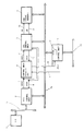
- the designation 1 is used in the drawing for an I/O unit, and 2 for an associated control unit.
- the I/O unit 1 is a secondary memory unit in the example shown here, although all I/O units which transfer data are possible.
- the control unit 2 is so arranged as to handle the transfer of data between the special interface of the I/O unit 1 and a general interface intended for connection to a bus 14, where direct memory access (DMA) is used for data transfer.
- DMA direct memory access
- the expression interface is used here to denote both the circuit solutions and the rules (protocols) required for data transfer.
- the I/O unit 1 is connected in the example illustrated in the drawing to the control unit 2 with the previously disclosed SCSI interface, although the use of other interfaces is possible.
- the designation 3 is used for a control unit for a system bus 13, and 4 for a directly addressable memory.
- the control unit 3 is so arranged as to handle the transfer of data between the system bus 13 and the local bus 14, where DMA can be used for the transfer of data.
- the control unit 3 includes a First-In-First-Out (FIFO) memory 3' for the equalization of the transfer rates between the system bus 13 and the local bus 14.
- FIFO First-In-First-Out
- the interface used for the system bus 13 is of the EISA (Extended Industry System Architecture) type, although control units for buses with other interfaces can be used.
- the memory 4 is connected via the bus 14 and is used here as a cache, although other applications are also possible.
- a control unit for multi-channel DMA is designated in the drawing as 5, and 6 is used to designate a control unit so arranged as to permit the transfer of data between the control unit 2 and the control unit 3.
- the embodiment illustrated in the drawing makes use of three channels, each of which has a DREQ n signal, namely on lines 7, 9 and 11 for DREQ 0 , DREQ 1 and DREQ 2 , in order to indicate that the control unit connected to the signal is ready to transfer data, as well as a DACK n signal, namely on lines 8, 10 and 12 for DACK 0 , DACK 1 and DACK 2 , which is activated by the DMA control unit 5 when transfer can take place.
- the control unit 5 uses write and read signals, WR and RD, intended for the local memory 4.
- the transfer of data between the control unit 2 of the I/O unit 1 and the control unit 3 of the system bus 13 is achieved by activating the DREQ 2 signal 11 connected to the DMA control unit 5 only when the DREQ 0 and DREQ 1 signals are active at the same time.
- the two DACK signals, DACK 0 and DACK 2 are activated in the same way when the DMA control unit 5 activates the DACK 2 signal.
- the possibility of transferring data between two DMA units, each of which is capable of transferring data only to and from a single memory, is thus achieved by using the DMA control unit 5 for bus arbitration and causing the control unit 6 to synchronize the DREQ signals from the two control units 2 and 3 in such a way that the transfer of data only takes place when both units are ready.
- a dedicated DMA channel is used for this purpose.
- the control unit 6 will terminate the transfer of data in those cases in which a local memory is not involved.
- the invention also includes other applications with a DMA control unit and DMA slaves used in conjunction with a control unit for a system bus. These then have the effect of changing the control in such a way that transfer takes place directly or indirectly between the slaves. The DMA control unit and the slaves involved are thus "tricked” into believing that normal DMA transfer is taking place.
- control unit 6 may be constructed in many different ways within the scope of the invention in order to operate in the manner described.
Abstract
Description
Claims (3)
- Arrangement for the transfer of data between data-transmitting and data-receiving units (1) connected to a common data bus (15), in conjunction with which the arrangement comprises a directly addressable memory (4) and a unit for direct memory access (5) so arranged as to control the transfer of data between the aforementioned data-transmitting and data-receiving units (1), characterized in that a control unit (6) is connected to the aforementioned data-transmitting, data-receiving (1) and direct memory access, or DMA (15) units and is so arranged, in conjunction with the transfer of data from a data-transmitting unit to a data-receiving unit, as to cause the data transfer also to include the simultaneous transfer of data to the directly addressable memory (4).
- Arrangement in accordance with Patent Claim 1, characterized in that the control unit (6) is so arranged as to synchronize the Data Request or DREQ and Data Acknowledge or DACK signals from the slaves allocated to the data units and to the directly addressable memory (4) in such a way that the transfer of data occurs only when the data-receiving unit and the directly addressable memory (4) are both ready for this to take place.
- Arrangement in accordance with Patent Claim 2, characterized in that the control unit (6) is connected on the one hand with the DREQ and DACK connections of the data-transmitting units, and on the other hand with the DMA unit via an additional arrangement of conventionally available DREQ-DACK connections to the DMA control unit (5) and is so arranged as to activate the DREQ signal on the additional connection of the DMA control unit (5) when the DREQ signals of the data-transferring units are both active, and as to activate the DACK signals of the data-transferring units when the DMA control unit has activated the additional connection.
Applications Claiming Priority (3)
| Application Number | Priority Date | Filing Date | Title |
|---|---|---|---|
| SE9103450A SE9103450L (en) | 1991-11-21 | 1991-11-21 | DEVICE FOR TRANSFER OF DATA BETWEEN DATA SENDING AND RECEIVING DEVICES CONNECTED TO A SHARED DATA BUS. |
| SE9103450 | 1991-11-21 | ||
| PCT/SE1992/000783 WO1993010499A1 (en) | 1991-11-21 | 1992-11-13 | Device for transmission of data |
Publications (2)
| Publication Number | Publication Date |
|---|---|
| EP0568678A1 EP0568678A1 (en) | 1993-11-10 |
| EP0568678B1 true EP0568678B1 (en) | 1998-06-10 |
Family
ID=20384396
Family Applications (1)
| Application Number | Title | Priority Date | Filing Date |
|---|---|---|---|
| EP92924081A Expired - Lifetime EP0568678B1 (en) | 1991-11-21 | 1992-11-13 | Device for transmission of data |
Country Status (5)
| Country | Link |
|---|---|
| EP (1) | EP0568678B1 (en) |
| DE (1) | DE69225883T2 (en) |
| FI (1) | FI103078B (en) |
| SE (1) | SE9103450L (en) |
| WO (1) | WO1993010499A1 (en) |
Families Citing this family (1)
| Publication number | Priority date | Publication date | Assignee | Title |
|---|---|---|---|---|
| KR100708096B1 (en) | 2000-07-21 | 2007-04-16 | 삼성전자주식회사 | Bus system and execution scheduling method for access commands thereof |
Family Cites Families (4)
| Publication number | Priority date | Publication date | Assignee | Title |
|---|---|---|---|---|
| US4782439A (en) * | 1987-02-17 | 1988-11-01 | Intel Corporation | Direct memory access system for microcontroller |
| JPH0233645A (en) * | 1988-07-22 | 1990-02-02 | Mitsubishi Electric Corp | Computer |
| JPH02226454A (en) * | 1989-01-13 | 1990-09-10 | Internatl Business Mach Corp <Ibm> | Computer system and transfer of data |
| JPH077955B2 (en) * | 1989-05-13 | 1995-01-30 | 株式会社東芝 | Data communication controller |
-
1991
- 1991-11-21 SE SE9103450A patent/SE9103450L/en not_active IP Right Cessation
-
1992
- 1992-11-13 WO PCT/SE1992/000783 patent/WO1993010499A1/en active IP Right Grant
- 1992-11-13 DE DE69225883T patent/DE69225883T2/en not_active Expired - Fee Related
- 1992-11-13 EP EP92924081A patent/EP0568678B1/en not_active Expired - Lifetime
-
1993
- 1993-07-21 FI FI933288A patent/FI103078B/en active
Also Published As
| Publication number | Publication date |
|---|---|
| FI933288A0 (en) | 1993-07-21 |
| SE468570B (en) | 1993-02-08 |
| SE9103450D0 (en) | 1991-11-21 |
| SE9103450L (en) | 1993-02-08 |
| FI103078B1 (en) | 1999-04-15 |
| DE69225883D1 (en) | 1998-07-16 |
| FI933288A (en) | 1993-07-21 |
| FI103078B (en) | 1999-04-15 |
| EP0568678A1 (en) | 1993-11-10 |
| WO1993010499A1 (en) | 1993-05-27 |
| DE69225883T2 (en) | 1998-10-08 |
Similar Documents
| Publication | Publication Date | Title |
|---|---|---|
| EP1646925B1 (en) | Apparatus and method for direct memory access in a hub-based memory system | |
| US4860244A (en) | Buffer system for input/output portion of digital data processing system | |
| JP3598321B2 (en) | Buffering data exchanged between buses operating at different frequencies | |
| US5274795A (en) | Peripheral I/O bus and programmable bus interface for computer data acquisition | |
| EP0834816A3 (en) | Microprocessor architecture capable of supporting multiple heterogenous processors | |
| MY109414A (en) | Bus interface logic for computer system having dual bus architecture | |
| US6892266B2 (en) | Multicore DSP device having coupled subsystem memory buses for global DMA access | |
| US5717875A (en) | Computing device having semi-dedicated high speed bus | |
| US4878173A (en) | Controller burst multiplexor channel interface | |
| EP0568678B1 (en) | Device for transmission of data | |
| EP0192578A3 (en) | A multiple bus system including a microprocessor having separate instruction and data interfaces and caches | |
| JPH08314854A (en) | Data transfer system and device relating to the same | |
| US5003461A (en) | Cluster controller memory arbiter | |
| US6609179B1 (en) | Method and apparatus for controlling memory access | |
| JPH09223103A (en) | Information processing system | |
| EP0439594B1 (en) | Device for interfacing a main processor bus connected to a main processor to a peripheral bus having a number of peripheral devices connected thereto | |
| JPH0553902A (en) | Memory control circuit | |
| JP2574821B2 (en) | Direct memory access controller | |
| JP2565916B2 (en) | Memory access controller | |
| JPS6217879Y2 (en) | ||
| JPH02211571A (en) | Information processor | |
| KR960032662A (en) | Synchronous / Asynchronous Bus Interface | |
| TW320699B (en) | Multi-channel direct memory access control circuit with distributed prefetch buffer | |
| KR950020095A (en) | DMA controller improves data transfer capacity | |
| JPH0113575B2 (en) |
Legal Events
| Date | Code | Title | Description |
|---|---|---|---|
| PUAI | Public reference made under article 153(3) epc to a published international application that has entered the european phase |
Free format text: ORIGINAL CODE: 0009012 |
|
| 17P | Request for examination filed |
Effective date: 19930707 |
|
| AK | Designated contracting states |
Kind code of ref document: A1 Designated state(s): DE GB |
|
| GRAG | Despatch of communication of intention to grant |
Free format text: ORIGINAL CODE: EPIDOS AGRA |
|
| 17Q | First examination report despatched |
Effective date: 19970623 |
|
| GRAG | Despatch of communication of intention to grant |
Free format text: ORIGINAL CODE: EPIDOS AGRA |
|
| GRAH | Despatch of communication of intention to grant a patent |
Free format text: ORIGINAL CODE: EPIDOS IGRA |
|
| RAP1 | Party data changed (applicant data changed or rights of an application transferred) |
Owner name: ICL SYSTEMS AKTIEBOLAG |
|
| GRAH | Despatch of communication of intention to grant a patent |
Free format text: ORIGINAL CODE: EPIDOS IGRA |
|
| GRAA | (expected) grant |
Free format text: ORIGINAL CODE: 0009210 |
|
| AK | Designated contracting states |
Kind code of ref document: B1 Designated state(s): DE GB |
|
| REF | Corresponds to: |
Ref document number: 69225883 Country of ref document: DE Date of ref document: 19980716 |
|
| PLBE | No opposition filed within time limit |
Free format text: ORIGINAL CODE: 0009261 |
|
| STAA | Information on the status of an ep patent application or granted ep patent |
Free format text: STATUS: NO OPPOSITION FILED WITHIN TIME LIMIT |
|
| 26N | No opposition filed | ||
| REG | Reference to a national code |
Ref country code: GB Ref legal event code: IF02 |
|
| PGFP | Annual fee paid to national office [announced via postgrant information from national office to epo] |
Ref country code: GB Payment date: 20031001 Year of fee payment: 12 |
|
| PGFP | Annual fee paid to national office [announced via postgrant information from national office to epo] |
Ref country code: DE Payment date: 20031027 Year of fee payment: 12 |
|
| PG25 | Lapsed in a contracting state [announced via postgrant information from national office to epo] |
Ref country code: GB Free format text: LAPSE BECAUSE OF NON-PAYMENT OF DUE FEES Effective date: 20041113 |
|
| PG25 | Lapsed in a contracting state [announced via postgrant information from national office to epo] |
Ref country code: DE Free format text: LAPSE BECAUSE OF NON-PAYMENT OF DUE FEES Effective date: 20050601 |
|
| GBPC | Gb: european patent ceased through non-payment of renewal fee |
Effective date: 20041113 |