EP0563605B1 - Procédé pour obtenir des microstructures - Google Patents
Procédé pour obtenir des microstructures Download PDFInfo
- Publication number
- EP0563605B1 EP0563605B1 EP93103431A EP93103431A EP0563605B1 EP 0563605 B1 EP0563605 B1 EP 0563605B1 EP 93103431 A EP93103431 A EP 93103431A EP 93103431 A EP93103431 A EP 93103431A EP 0563605 B1 EP0563605 B1 EP 0563605B1
- Authority
- EP
- European Patent Office
- Prior art keywords
- etching
- effected
- value
- track
- particle
- Prior art date
- Legal status (The legal status is an assumption and is not a legal conclusion. Google has not performed a legal analysis and makes no representation as to the accuracy of the status listed.)
- Expired - Lifetime
Links
- 238000000034 method Methods 0.000 title claims description 38
- 238000004519 manufacturing process Methods 0.000 title description 9
- 238000005530 etching Methods 0.000 claims description 78
- 239000002245 particle Substances 0.000 claims description 24
- 230000008569 process Effects 0.000 claims description 12
- 239000004642 Polyimide Substances 0.000 claims description 7
- 229920001721 polyimide Polymers 0.000 claims description 7
- 150000002500 ions Chemical class 0.000 claims description 6
- 239000007787 solid Substances 0.000 claims description 6
- 230000007935 neutral effect Effects 0.000 claims description 4
- 230000003647 oxidation Effects 0.000 claims description 4
- 238000007254 oxidation reaction Methods 0.000 claims description 4
- 230000001678 irradiating effect Effects 0.000 claims description 2
- 230000001105 regulatory effect Effects 0.000 claims description 2
- 239000012530 fluid Substances 0.000 claims 2
- 238000012544 monitoring process Methods 0.000 claims 1
- 239000000463 material Substances 0.000 description 18
- 239000007788 liquid Substances 0.000 description 9
- 239000011148 porous material Substances 0.000 description 5
- 239000012634 fragment Substances 0.000 description 4
- 229920003223 poly(pyromellitimide-1,4-diphenyl ether) Polymers 0.000 description 4
- 239000000243 solution Substances 0.000 description 3
- ZAMOUSCENKQFHK-UHFFFAOYSA-N Chlorine atom Chemical compound [Cl] ZAMOUSCENKQFHK-UHFFFAOYSA-N 0.000 description 2
- 239000007864 aqueous solution Substances 0.000 description 2
- 239000007844 bleaching agent Substances 0.000 description 2
- 230000008859 change Effects 0.000 description 2
- 239000000460 chlorine Substances 0.000 description 2
- 229910052801 chlorine Inorganic materials 0.000 description 2
- 238000012423 maintenance Methods 0.000 description 2
- 238000005457 optimization Methods 0.000 description 2
- 229920000642 polymer Polymers 0.000 description 2
- 230000009467 reduction Effects 0.000 description 2
- 238000003860 storage Methods 0.000 description 2
- 206010070834 Sensitisation Diseases 0.000 description 1
- 239000005708 Sodium hypochlorite Substances 0.000 description 1
- QVGXLLKOCUKJST-UHFFFAOYSA-N atomic oxygen Chemical compound [O] QVGXLLKOCUKJST-UHFFFAOYSA-N 0.000 description 1
- 230000001276 controlling effect Effects 0.000 description 1
- 238000005516 engineering process Methods 0.000 description 1
- 230000004992 fission Effects 0.000 description 1
- 239000010931 gold Substances 0.000 description 1
- 229910052737 gold Inorganic materials 0.000 description 1
- -1 gold ions Chemical class 0.000 description 1
- 238000009499 grossing Methods 0.000 description 1
- 230000035876 healing Effects 0.000 description 1
- 239000011810 insulating material Substances 0.000 description 1
- 239000001301 oxygen Substances 0.000 description 1
- 229910052760 oxygen Inorganic materials 0.000 description 1
- 230000037361 pathway Effects 0.000 description 1
- 229920006254 polymer film Polymers 0.000 description 1
- 230000005855 radiation Effects 0.000 description 1
- 230000005070 ripening Effects 0.000 description 1
- 238000007788 roughening Methods 0.000 description 1
- 238000001878 scanning electron micrograph Methods 0.000 description 1
- 230000008313 sensitization Effects 0.000 description 1
- 238000004904 shortening Methods 0.000 description 1
- SUKJFIGYRHOWBL-UHFFFAOYSA-N sodium hypochlorite Chemical compound [Na+].Cl[O-] SUKJFIGYRHOWBL-UHFFFAOYSA-N 0.000 description 1
- 239000007858 starting material Substances 0.000 description 1
- 239000000126 substance Substances 0.000 description 1
- 230000007704 transition Effects 0.000 description 1
- 238000003631 wet chemical etching Methods 0.000 description 1
- 238000007704 wet chemistry method Methods 0.000 description 1
Images


Classifications
-
- H—ELECTRICITY
- H01—ELECTRIC ELEMENTS
- H01L—SEMICONDUCTOR DEVICES NOT COVERED BY CLASS H10
- H01L21/00—Processes or apparatus adapted for the manufacture or treatment of semiconductor or solid state devices or of parts thereof
- H01L21/02—Manufacture or treatment of semiconductor devices or of parts thereof
- H01L21/04—Manufacture or treatment of semiconductor devices or of parts thereof the devices having potential barriers, e.g. a PN junction, depletion layer or carrier concentration layer
- H01L21/18—Manufacture or treatment of semiconductor devices or of parts thereof the devices having potential barriers, e.g. a PN junction, depletion layer or carrier concentration layer the devices having semiconductor bodies comprising elements of Group IV of the Periodic Table or AIIIBV compounds with or without impurities, e.g. doping materials
- H01L21/30—Treatment of semiconductor bodies using processes or apparatus not provided for in groups H01L21/20 - H01L21/26
- H01L21/31—Treatment of semiconductor bodies using processes or apparatus not provided for in groups H01L21/20 - H01L21/26 to form insulating layers thereon, e.g. for masking or by using photolithographic techniques; After treatment of these layers; Selection of materials for these layers
- H01L21/3105—After-treatment
- H01L21/311—Etching the insulating layers by chemical or physical means
- H01L21/31127—Etching organic layers
- H01L21/31133—Etching organic layers by chemical means
-
- B—PERFORMING OPERATIONS; TRANSPORTING
- B01—PHYSICAL OR CHEMICAL PROCESSES OR APPARATUS IN GENERAL
- B01D—SEPARATION
- B01D67/00—Processes specially adapted for manufacturing semi-permeable membranes for separation processes or apparatus
- B01D67/0002—Organic membrane manufacture
- B01D67/0023—Organic membrane manufacture by inducing porosity into non porous precursor membranes
- B01D67/0032—Organic membrane manufacture by inducing porosity into non porous precursor membranes by elimination of segments of the precursor, e.g. nucleation-track membranes, lithography or laser methods
-
- B—PERFORMING OPERATIONS; TRANSPORTING
- B01—PHYSICAL OR CHEMICAL PROCESSES OR APPARATUS IN GENERAL
- B01J—CHEMICAL OR PHYSICAL PROCESSES, e.g. CATALYSIS OR COLLOID CHEMISTRY; THEIR RELEVANT APPARATUS
- B01J19/00—Chemical, physical or physico-chemical processes in general; Their relevant apparatus
- B01J19/08—Processes employing the direct application of electric or wave energy, or particle radiation; Apparatus therefor
- B01J19/081—Processes employing the direct application of electric or wave energy, or particle radiation; Apparatus therefor employing particle radiation or gamma-radiation
-
- B—PERFORMING OPERATIONS; TRANSPORTING
- B29—WORKING OF PLASTICS; WORKING OF SUBSTANCES IN A PLASTIC STATE IN GENERAL
- B29C—SHAPING OR JOINING OF PLASTICS; SHAPING OF MATERIAL IN A PLASTIC STATE, NOT OTHERWISE PROVIDED FOR; AFTER-TREATMENT OF THE SHAPED PRODUCTS, e.g. REPAIRING
- B29C59/00—Surface shaping of articles, e.g. embossing; Apparatus therefor
- B29C59/16—Surface shaping of articles, e.g. embossing; Apparatus therefor by wave energy or particle radiation, e.g. infrared heating
-
- B—PERFORMING OPERATIONS; TRANSPORTING
- B29—WORKING OF PLASTICS; WORKING OF SUBSTANCES IN A PLASTIC STATE IN GENERAL
- B29C—SHAPING OR JOINING OF PLASTICS; SHAPING OF MATERIAL IN A PLASTIC STATE, NOT OTHERWISE PROVIDED FOR; AFTER-TREATMENT OF THE SHAPED PRODUCTS, e.g. REPAIRING
- B29C71/00—After-treatment of articles without altering their shape; Apparatus therefor
- B29C71/04—After-treatment of articles without altering their shape; Apparatus therefor by wave energy or particle radiation, e.g. for curing or vulcanising preformed articles
-
- C—CHEMISTRY; METALLURGY
- C08—ORGANIC MACROMOLECULAR COMPOUNDS; THEIR PREPARATION OR CHEMICAL WORKING-UP; COMPOSITIONS BASED THEREON
- C08J—WORKING-UP; GENERAL PROCESSES OF COMPOUNDING; AFTER-TREATMENT NOT COVERED BY SUBCLASSES C08B, C08C, C08F, C08G or C08H
- C08J9/00—Working-up of macromolecular substances to porous or cellular articles or materials; After-treatment thereof
- C08J9/26—Working-up of macromolecular substances to porous or cellular articles or materials; After-treatment thereof by elimination of a solid phase from a macromolecular composition or article, e.g. leaching out
-
- C—CHEMISTRY; METALLURGY
- C23—COATING METALLIC MATERIAL; COATING MATERIAL WITH METALLIC MATERIAL; CHEMICAL SURFACE TREATMENT; DIFFUSION TREATMENT OF METALLIC MATERIAL; COATING BY VACUUM EVAPORATION, BY SPUTTERING, BY ION IMPLANTATION OR BY CHEMICAL VAPOUR DEPOSITION, IN GENERAL; INHIBITING CORROSION OF METALLIC MATERIAL OR INCRUSTATION IN GENERAL
- C23F—NON-MECHANICAL REMOVAL OF METALLIC MATERIAL FROM SURFACE; INHIBITING CORROSION OF METALLIC MATERIAL OR INCRUSTATION IN GENERAL; MULTI-STEP PROCESSES FOR SURFACE TREATMENT OF METALLIC MATERIAL INVOLVING AT LEAST ONE PROCESS PROVIDED FOR IN CLASS C23 AND AT LEAST ONE PROCESS COVERED BY SUBCLASS C21D OR C22F OR CLASS C25
- C23F4/00—Processes for removing metallic material from surfaces, not provided for in group C23F1/00 or C23F3/00
-
- G—PHYSICS
- G03—PHOTOGRAPHY; CINEMATOGRAPHY; ANALOGOUS TECHNIQUES USING WAVES OTHER THAN OPTICAL WAVES; ELECTROGRAPHY; HOLOGRAPHY
- G03F—PHOTOMECHANICAL PRODUCTION OF TEXTURED OR PATTERNED SURFACES, e.g. FOR PRINTING, FOR PROCESSING OF SEMICONDUCTOR DEVICES; MATERIALS THEREFOR; ORIGINALS THEREFOR; APPARATUS SPECIALLY ADAPTED THEREFOR
- G03F7/00—Photomechanical, e.g. photolithographic, production of textured or patterned surfaces, e.g. printing surfaces; Materials therefor, e.g. comprising photoresists; Apparatus specially adapted therefor
- G03F7/004—Photosensitive materials
- G03F7/039—Macromolecular compounds which are photodegradable, e.g. positive electron resists
-
- H—ELECTRICITY
- H01—ELECTRIC ELEMENTS
- H01L—SEMICONDUCTOR DEVICES NOT COVERED BY CLASS H10
- H01L21/00—Processes or apparatus adapted for the manufacture or treatment of semiconductor or solid state devices or of parts thereof
- H01L21/02—Manufacture or treatment of semiconductor devices or of parts thereof
- H01L21/027—Making masks on semiconductor bodies for further photolithographic processing not provided for in group H01L21/18 or H01L21/34
- H01L21/0271—Making masks on semiconductor bodies for further photolithographic processing not provided for in group H01L21/18 or H01L21/34 comprising organic layers
- H01L21/0273—Making masks on semiconductor bodies for further photolithographic processing not provided for in group H01L21/18 or H01L21/34 comprising organic layers characterised by the treatment of photoresist layers
- H01L21/0279—Ionlithographic processes
-
- B—PERFORMING OPERATIONS; TRANSPORTING
- B01—PHYSICAL OR CHEMICAL PROCESSES OR APPARATUS IN GENERAL
- B01D—SEPARATION
- B01D2323/00—Details relating to membrane preparation
- B01D2323/08—Specific temperatures applied
-
- B—PERFORMING OPERATIONS; TRANSPORTING
- B29—WORKING OF PLASTICS; WORKING OF SUBSTANCES IN A PLASTIC STATE IN GENERAL
- B29C—SHAPING OR JOINING OF PLASTICS; SHAPING OF MATERIAL IN A PLASTIC STATE, NOT OTHERWISE PROVIDED FOR; AFTER-TREATMENT OF THE SHAPED PRODUCTS, e.g. REPAIRING
- B29C35/00—Heating, cooling or curing, e.g. crosslinking or vulcanising; Apparatus therefor
- B29C35/02—Heating or curing, e.g. crosslinking or vulcanizing during moulding, e.g. in a mould
- B29C35/08—Heating or curing, e.g. crosslinking or vulcanizing during moulding, e.g. in a mould by wave energy or particle radiation
- B29C35/0866—Heating or curing, e.g. crosslinking or vulcanizing during moulding, e.g. in a mould by wave energy or particle radiation using particle radiation
- B29C2035/0872—Heating or curing, e.g. crosslinking or vulcanizing during moulding, e.g. in a mould by wave energy or particle radiation using particle radiation using ion-radiation, e.g. alpha-rays
-
- B—PERFORMING OPERATIONS; TRANSPORTING
- B29—WORKING OF PLASTICS; WORKING OF SUBSTANCES IN A PLASTIC STATE IN GENERAL
- B29K—INDEXING SCHEME ASSOCIATED WITH SUBCLASSES B29B, B29C OR B29D, RELATING TO MOULDING MATERIALS OR TO MATERIALS FOR MOULDS, REINFORCEMENTS, FILLERS OR PREFORMED PARTS, e.g. INSERTS
- B29K2079/00—Use of polymers having nitrogen, with or without oxygen or carbon only, in the main chain, not provided for in groups B29K2061/00 - B29K2077/00, as moulding material
- B29K2079/08—PI, i.e. polyimides or derivatives thereof
-
- C—CHEMISTRY; METALLURGY
- C08—ORGANIC MACROMOLECULAR COMPOUNDS; THEIR PREPARATION OR CHEMICAL WORKING-UP; COMPOSITIONS BASED THEREON
- C08J—WORKING-UP; GENERAL PROCESSES OF COMPOUNDING; AFTER-TREATMENT NOT COVERED BY SUBCLASSES C08B, C08C, C08F, C08G or C08H
- C08J2201/00—Foams characterised by the foaming process
- C08J2201/04—Foams characterised by the foaming process characterised by the elimination of a liquid or solid component, e.g. precipitation, leaching out, evaporation
- C08J2201/046—Elimination of a polymeric phase
-
- C—CHEMISTRY; METALLURGY
- C08—ORGANIC MACROMOLECULAR COMPOUNDS; THEIR PREPARATION OR CHEMICAL WORKING-UP; COMPOSITIONS BASED THEREON
- C08J—WORKING-UP; GENERAL PROCESSES OF COMPOUNDING; AFTER-TREATMENT NOT COVERED BY SUBCLASSES C08B, C08C, C08F, C08G or C08H
- C08J2379/00—Characterised by the use of macromolecular compounds obtained by reactions forming in the main chain of the macromolecule a linkage containing nitrogen with or without oxygen, or carbon only, not provided for in groups C08J2361/00 - C08J2377/00
- C08J2379/04—Polycondensates having nitrogen-containing heterocyclic rings in the main chain; Polyhydrazides; Polyamide acids or similar polyimide precursors
- C08J2379/08—Polyimides; Polyester-imides; Polyamide-imides; Polyamide acids or similar polyimide precursors
Definitions
- the present invention relates to a method for producing microstructures such as microholes or channels in insulating solids, preferably made of polyimide, by irradiating the solid with ions of a predetermined atomic number, density and energy, with subsequent ripening of the particle tracks by oxidation processes and subsequent etching of the ripened particle tracks in aqueous etching solution.
- the selectivity S of the particle track etching with an etching liquid acting on the irradiated surface is defined as the ratio of the track etching rate V T to the etching rate V B of the undisturbed material.
- the track etching rate V T is the etching rate along a particle track and the material etching rate V B is the etching rate in the material transverse to the track. Both etch rates overlap.
- the present invention has the task of specifying a method for producing microstructures which no longer has the disadvantages mentioned and with which more optimal structures can be produced.
- the method should enable the production of microstructures whose geometry can be predetermined and whose pores have, for example, more uniform diameters and / or which have walls that are as smooth and parallel as possible.
- the present invention now proposes, in a method of the type described in the introduction, the method step which is stated in the characterizing part. Further advantageous process steps can be seen in the features of the subclaims.
- the method according to the invention is based on the new and surprising finding that the selectivity in an etching in aqueous solution depends on the pH of the same.
- structures can now be generated whose geometry can be exactly predetermined. This can be used to achieve exactly parallel-walled channels, for example. Tapered micropores as well as those in the form of a hollow hollow cylinder can also be produced.
- a shortening for the pore-enlarging etching process can be achieved by a suitable choice of the pH value.
- the material throughput in the etching bath can be increased as a result. The procedure creates smooth material surfaces and smooth perforated walls in the structures.
- the cone diameter in the case of conical structures can be adjusted by selecting the selectivity via the pH value, since the increase in the material etching rate is always associated with a reduction in the selectivity of the etching process in the latent particle traces. This then enlarges the etching cone and creates conical etching pores.
- the separate optimization of selectivity and smoothing in the production of microstructures using the track etching technique is new and particularly advantageous.
- the method is particularly well suited for insulating materials, such as preferably polyimide.
- Steps a) and b) here are the same as those in the method described in FIG. 1.
- a latent particle track 4 is generated in step a) by irradiation in the film 1 with the inhomogeneities 5, which is matured in step b) by oxidation processes.
- the inhomogeneities 5 remain unchanged.
- the selectivity S depends on the pH of the aqueous etching solution.
- the selectivity S is the quotient or the ratio of the track etching rate V T and the material etching rate V B and these in turn depend linearly or exponentially on the pH value.
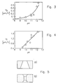
- FIGS. 3 and 4 the FIG. 3 the material etching rate V B of the polyimide Kapton (trademark DuPont) with an exponential increase and the FIG. 4 the track etching rate V T of the same material with a linear increase depending on the pH value of the etching liquid shows. Both etch rates overlap. From this it is now readily apparent that by gradually varying the pH of the etching liquid, the etching rates are influenced in many ways can be. Depending on the respective etching rate, a very specific desired shape of the structure to be etched results.
- step c a kind of selective pre-etching.
- short fragments of the molecular chains are now selectively removed, in the form shown with a high track etching rate V T , ie the particle track 4 is "narrowly cleared", so to speak.
- V T high track etching rate
- a first stage of a kind of pre-etching can be set so that the inhomogeneities 5 remain unchanged. Zones up to approximately 100 times the atomic or molecular diameter are preferably extracted.
- the particle track 6 thus pre-etched in the first stage is then subjected to a second etching stage in accordance with step d), in the illustration shown a smooth re-etching.
- the pre-etched particle track 6 is expanded to the desired diameter 7. This can be done, for example, by greatly increasing the material etching rate V B (for example pH values above 10).
- V B for example pH values above 10
- the inhomogeneities 5 are removed evenly.
- the transition between the two stages c) and d) shown here can take place, for example, by a discontinuous change in the pH in the same etching liquid or by different etching liquids with different pH values.
- the setting and maintenance can also be achieved by means of continuous control by a regulated dosing system.
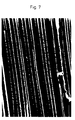
- FIG. 6 shows the surface, in FIG. 7, the fracture surface of such a Kapton filter, which was produced according to the following exemplary embodiment and is microscopically enlarged.
- the hole diameters fluctuate only slightly, the track channels are almost parallel-walled:
- a 50 ⁇ m thick polymide film (Kapton) was irradiated with 11 MeV / nucleon gold ions at an areal density of 107 ions / cm2.
- the pre-etched channels were etched to 1 ⁇ m hole diameter in 1.5 hours.
- the pore structure formed is shown enlarged in FIGS. 6 and 7.
- FIG. 5 shows two further, special basic shapes of pores which can be produced using the new method.
- a) shows a truncated cone by one-sided etching from below and b) a chamfered hollow cylinder. This is generated by pre-etching with low and post-etching with high selectivity.
- a continuous change in the etching liquid is also possible.
Landscapes
- Chemical & Material Sciences (AREA)
- Engineering & Computer Science (AREA)
- Physics & Mathematics (AREA)
- Chemical Kinetics & Catalysis (AREA)
- General Physics & Mathematics (AREA)
- Health & Medical Sciences (AREA)
- Manufacturing & Machinery (AREA)
- Organic Chemistry (AREA)
- Power Engineering (AREA)
- Condensed Matter Physics & Semiconductors (AREA)
- Materials Engineering (AREA)
- Microelectronics & Electronic Packaging (AREA)
- Computer Hardware Design (AREA)
- Toxicology (AREA)
- General Chemical & Material Sciences (AREA)
- General Health & Medical Sciences (AREA)
- Metallurgy (AREA)
- Mechanical Engineering (AREA)
- Spectroscopy & Molecular Physics (AREA)
- Medicinal Chemistry (AREA)
- Polymers & Plastics (AREA)
- Optics & Photonics (AREA)
- Treatments Of Macromolecular Shaped Articles (AREA)
- Micromachines (AREA)
- Weting (AREA)
- Separation Using Semi-Permeable Membranes (AREA)
Claims (6)
- Procédé pour former les microstructures telles que des microtrous, ou des microcanaux dans des corps solides isolants, de préférence en polyimide, par irradiation du corps solide avec des ions ayant un numéro aotmique, une densité et une énergie déterminés, et une maturation consécutive des traces de particules par des procédés d'oxydation suivis d'une attaque des traces des particules ayant mûris, dans une solution aqueuse d'attaque, caractérisé en ce qu'on modifie la valeur de pH de la solution pendant l'attaque pour la faire passer par plusieurs valeurs.
- Procédé selon la revendication 1, caractérisé en ce que la variation se fait par étapes suivant des valeurs délimitées.
- Procédé selon la revendication 1, caractérisé en ce que la variation est continue.
- Procédé selon la revendication 1, caractérisé en ce qu'on procède à une attaque chimique, tout d'abord à proximité du point neutre avec une valeur pH = 8, puis, loin du point neutre avec environ pH = 12.
- Procédé selon la revendication 2, caractérisé en ce qu'on règle et on maintient la valeur pH des étapes par adjonction d'un agent tampon au liquide d'attaque.
- Procédé selon les revendications 1, 2 ou 3, caractérisé en ce qu'on règle et on maintient la valeur pH du liquide d'attaque par un contrôle continu au moyen d'un système de dosage à régulation par réaction.
Applications Claiming Priority (2)
| Application Number | Priority Date | Filing Date | Title |
|---|---|---|---|
| DE4210486 | 1992-03-31 | ||
| DE4210486A DE4210486C1 (fr) | 1992-03-31 | 1992-03-31 |
Publications (2)
| Publication Number | Publication Date |
|---|---|
| EP0563605A1 EP0563605A1 (fr) | 1993-10-06 |
| EP0563605B1 true EP0563605B1 (fr) | 1995-10-18 |
Family
ID=6455483
Family Applications (1)
| Application Number | Title | Priority Date | Filing Date |
|---|---|---|---|
| EP93103431A Expired - Lifetime EP0563605B1 (fr) | 1992-03-31 | 1993-03-03 | Procédé pour obtenir des microstructures |
Country Status (2)
| Country | Link |
|---|---|
| EP (1) | EP0563605B1 (fr) |
| DE (2) | DE4210486C1 (fr) |
Families Citing this family (5)
| Publication number | Priority date | Publication date | Assignee | Title |
|---|---|---|---|---|
| DE10058822A1 (de) * | 2000-11-27 | 2002-06-20 | Danziger Manfred | Verfahren zur Bearbeitung von Trägerfolien durch Bestrahlen mit Schwerionen |
| DE10208023A1 (de) * | 2002-02-26 | 2003-09-11 | Schwerionenforsch Gmbh | Verfahren zur Herstellung von Nanostrukturen in Membranen und asymmetrische Membran |
| US6908552B2 (en) | 2002-02-26 | 2005-06-21 | Gesellschaft Fuer Schwerionenforschung Mbh | Method of producing nanostructures in membrances, and asymmetrical membrane |
| DE10234614B3 (de) * | 2002-07-24 | 2004-03-04 | Fractal Ag | Verfahren zur Bearbeitung von Trägermaterial durch Schwerionenbestrahlung und nachfolgenden Ätzprozess |
| US10350854B2 (en) | 2011-06-08 | 2019-07-16 | BLüCHER GMBH | Functional protective material, in particular for use in protective clothing |
Family Cites Families (10)
| Publication number | Priority date | Publication date | Assignee | Title |
|---|---|---|---|---|
| FR1357143A (fr) * | 1962-02-28 | 1964-04-03 | Thomson Houston Comp Francaise | Nouveau produit et procédés de fabrication de pièces perforées |
| GB1271423A (en) * | 1968-06-27 | 1972-04-19 | Gen Electric | Improvements relating to the manufacture of sheets having holes therein by an etching process |
| US3852134A (en) * | 1969-05-05 | 1974-12-03 | Gen Electric | Method for forming selectively perforate bodies |
| US3713921A (en) * | 1971-04-01 | 1973-01-30 | Gen Electric | Geometry control of etched nuclear particle tracks |
| DE2140579A1 (de) * | 1971-08-13 | 1973-02-22 | Licentia Gmbh | Verfahren zum aufzeichnen von informationen entlang einer spiralfoermig verlaufenden spur eines informationstraegers |
| DE2541624C2 (de) * | 1975-09-18 | 1982-09-16 | Ibm Deutschland Gmbh, 7000 Stuttgart | Wässrige Ätzlösung und Verfahren zum Ätzen von Polymerfilmen oder Folien auf Polyimidbasis |
| US4648950A (en) * | 1985-10-15 | 1987-03-10 | The United States Of America As Represented By The United States Department Of Energy | CR-39 track etching and blow-up method |
| US4909896A (en) * | 1988-02-29 | 1990-03-20 | Hoya Corporation | Process for producing contact lens |
| DE3816078A1 (de) * | 1988-05-11 | 1989-11-23 | Brandt Reinhard | Verfahren zur herstellung hitzebestaendiger und chemikalienresistenter feinstporiger mikrosiebe (lichgroessen d > 10 nano-m) aus der polyimid-folie "kapton" (handelsname von du pont) |
| EP0364628B1 (fr) * | 1988-10-19 | 1996-08-28 | Arastoo Khodai Joopary | Séparations de gaz, d'isotopes et de liquides à l'aide de membranes |
-
1992
- 1992-03-31 DE DE4210486A patent/DE4210486C1/de not_active Expired - Fee Related
-
1993
- 1993-03-03 DE DE59300764T patent/DE59300764D1/de not_active Expired - Fee Related
- 1993-03-03 EP EP93103431A patent/EP0563605B1/fr not_active Expired - Lifetime
Non-Patent Citations (1)
| Title |
|---|
| DATABASE WPIL Week 9303, Derwent Publications Ltd., London, GB; AN 93-026182 & SU-A-1716458 (EREV. PHSY. INST.) 29. Februar 1992 * |
Also Published As
| Publication number | Publication date |
|---|---|
| DE4210486C1 (fr) | 1993-05-06 |
| EP0563605A1 (fr) | 1993-10-06 |
| DE59300764D1 (de) | 1995-11-23 |
Similar Documents
| Publication | Publication Date | Title |
|---|---|---|
| EP3022007B1 (fr) | Procédé de fabrication d'un noeud par soudage avec la même largeur pour deux soudures | |
| DE60101209T2 (de) | Verfahren und Vorrichtung zur sequentiellen Plasmabehandlung | |
| DE4433744C2 (de) | Vorrichtung zum Vermischen von Medien zur Erzeugung flüssiger Systeme | |
| DE2930391A1 (de) | Plasmaaetzvorrichtung | |
| WO2016041544A1 (fr) | Procédé d'insertion d'au moins un évidement ou trou débouchant dans une pièce en forme de plaque | |
| DE10200680A1 (de) | Minimale Schwingungsanregung beim Verfahren mit Ruckbegrenzung durch Adaption von Ruckprofilen | |
| EP1483435A1 (fr) | Filiere de fibres creuses | |
| EP0563605B1 (fr) | Procédé pour obtenir des microstructures | |
| DE102020114195A1 (de) | Verfahren zum Einbringen einer Ausnehmung in ein Substrat | |
| DE6919686U (de) | Filterkoerper aus metallfasern | |
| DE10139638A1 (de) | Anordnung zur Erzeugung von Führungsgrößen für Regelkreise einer numerisch gesteuerten Maschine | |
| DE10234614B3 (de) | Verfahren zur Bearbeitung von Trägermaterial durch Schwerionenbestrahlung und nachfolgenden Ätzprozess | |
| DE2117199C3 (de) | Verfahren zur Herstellung geätzter Muster in dünnen Schichten mit definierten Kantenprofilen | |
| DE2342470A1 (de) | Verfahren zum zerteilen eines fluessigkeitsstrahls, vorrichtung zur durchfuehrung dieses verfahrens und anwendung dieses verfahrens auf die granulierung eines zuvor verfluessigten produktes | |
| DE102019110507A1 (de) | Vorrichtung zur Behandlung einer Luftströmung mit einem nichtthermischen Plasma | |
| DE4413574C1 (de) | Membran zur Mikrofiltration von Suspensionen oder zur Gastrennung | |
| WO2013107858A1 (fr) | Procédé de fabrication d'une plaque de rupture | |
| DE2326007B2 (de) | Verfahren und Vorrichtung zur Steuerung der Elektrodenvorschubbewegung bei der elektroerosiven Bearbeitung | |
| EP2228121A1 (fr) | Dispositif d'enrichissement du gaz ou de production d'un service mécanique, ainsi que procédé correspondant | |
| DE3140755A1 (de) | Vorrichtung zum extrudieren eines fibrillierten vorproduktes | |
| DE3016622A1 (de) | Verfahren und vorrichtung zur herstellung von perforiertem papier | |
| DE3731823C2 (fr) | ||
| DE2658405C2 (de) | Dialysemembrane, insbesondere zur Hömodialyse, und Verfahren zu ihrer Herstellung | |
| BE1025471B1 (de) | Verfahren zur Herstellung eines Aktivelements und entsprechendes Aktivelement | |
| DE1952587C3 (de) | Verfahren zur Herstellung von Elektroden zur elektroerosiven Erzeugung von Profil-Spinnbohrungen |
Legal Events
| Date | Code | Title | Description |
|---|---|---|---|
| PUAI | Public reference made under article 153(3) epc to a published international application that has entered the european phase |
Free format text: ORIGINAL CODE: 0009012 |
|
| AK | Designated contracting states |
Kind code of ref document: A1 Designated state(s): CH DE FR GB IT LI NL |
|
| 17P | Request for examination filed |
Effective date: 19931110 |
|
| 17Q | First examination report despatched |
Effective date: 19950113 |
|
| GRAA | (expected) grant |
Free format text: ORIGINAL CODE: 0009210 |
|
| AK | Designated contracting states |
Kind code of ref document: B1 Designated state(s): CH DE FR GB IT LI NL |
|
| PG25 | Lapsed in a contracting state [announced via postgrant information from national office to epo] |
Ref country code: NL Free format text: LAPSE BECAUSE OF FAILURE TO SUBMIT A TRANSLATION OF THE DESCRIPTION OR TO PAY THE FEE WITHIN THE PRESCRIBED TIME-LIMIT Effective date: 19951018 Ref country code: IT Free format text: LAPSE BECAUSE OF FAILURE TO SUBMIT A TRANSLATION OF THE DESCRIPTION OR TO PAY THE FEE WITHIN THE PRESCRIBED TIME-LIMIT;WARNING: LAPSES OF ITALIAN PATENTS WITH EFFECTIVE DATE BEFORE 2007 MAY HAVE OCCURRED AT ANY TIME BEFORE 2007. THE CORRECT EFFECTIVE DATE MAY BE DIFFERENT FROM THE ONE RECORDED. Effective date: 19951018 |
|
| REF | Corresponds to: |
Ref document number: 59300764 Country of ref document: DE Date of ref document: 19951123 |
|
| ET | Fr: translation filed | ||
| GBT | Gb: translation of ep patent filed (gb section 77(6)(a)/1977) |
Effective date: 19951127 |
|
| NLV1 | Nl: lapsed or annulled due to failure to fulfill the requirements of art. 29p and 29m of the patents act | ||
| PG25 | Lapsed in a contracting state [announced via postgrant information from national office to epo] |
Ref country code: LI Effective date: 19960331 Ref country code: CH Effective date: 19960331 |
|
| PLBE | No opposition filed within time limit |
Free format text: ORIGINAL CODE: 0009261 |
|
| STAA | Information on the status of an ep patent application or granted ep patent |
Free format text: STATUS: NO OPPOSITION FILED WITHIN TIME LIMIT |
|
| 26N | No opposition filed | ||
| REG | Reference to a national code |
Ref country code: CH Ref legal event code: PL |
|
| REG | Reference to a national code |
Ref country code: GB Ref legal event code: IF02 |
|
| PGFP | Annual fee paid to national office [announced via postgrant information from national office to epo] |
Ref country code: DE Payment date: 20070302 Year of fee payment: 15 |
|
| PGFP | Annual fee paid to national office [announced via postgrant information from national office to epo] |
Ref country code: GB Payment date: 20070312 Year of fee payment: 15 |
|
| PGFP | Annual fee paid to national office [announced via postgrant information from national office to epo] |
Ref country code: FR Payment date: 20070329 Year of fee payment: 15 |
|
| GBPC | Gb: european patent ceased through non-payment of renewal fee |
Effective date: 20080303 |
|
| REG | Reference to a national code |
Ref country code: FR Ref legal event code: ST Effective date: 20081125 |
|
| PG25 | Lapsed in a contracting state [announced via postgrant information from national office to epo] |
Ref country code: DE Free format text: LAPSE BECAUSE OF NON-PAYMENT OF DUE FEES Effective date: 20081001 |
|
| PG25 | Lapsed in a contracting state [announced via postgrant information from national office to epo] |
Ref country code: FR Free format text: LAPSE BECAUSE OF NON-PAYMENT OF DUE FEES Effective date: 20080331 |
|
| PG25 | Lapsed in a contracting state [announced via postgrant information from national office to epo] |
Ref country code: GB Free format text: LAPSE BECAUSE OF NON-PAYMENT OF DUE FEES Effective date: 20080303 |