EP0561358B1 - Video control circuit for multimedia applications - Google Patents
Video control circuit for multimedia applications Download PDFInfo
- Publication number
- EP0561358B1 EP0561358B1 EP93104285A EP93104285A EP0561358B1 EP 0561358 B1 EP0561358 B1 EP 0561358B1 EP 93104285 A EP93104285 A EP 93104285A EP 93104285 A EP93104285 A EP 93104285A EP 0561358 B1 EP0561358 B1 EP 0561358B1
- Authority
- EP
- European Patent Office
- Prior art keywords
- output
- signals
- block
- multiplexer
- input
- Prior art date
- Legal status (The legal status is an assumption and is not a legal conclusion. Google has not performed a legal analysis and makes no representation as to the accuracy of the status listed.)
- Expired - Lifetime
Links
Images






Classifications
-
- H—ELECTRICITY
- H04—ELECTRIC COMMUNICATION TECHNIQUE
- H04N—PICTORIAL COMMUNICATION, e.g. TELEVISION
- H04N21/00—Selective content distribution, e.g. interactive television or video on demand [VOD]
- H04N21/40—Client devices specifically adapted for the reception of or interaction with content, e.g. set-top-box [STB]; Operations thereof
- H04N21/41—Structure of client; Structure of client peripherals
- H04N21/414—Specialised client platforms, e.g. receiver in car or embedded in a mobile appliance
- H04N21/4143—Specialised client platforms, e.g. receiver in car or embedded in a mobile appliance embedded in a Personal Computer [PC]
-
- H—ELECTRICITY
- H04—ELECTRIC COMMUNICATION TECHNIQUE
- H04N—PICTORIAL COMMUNICATION, e.g. TELEVISION
- H04N9/00—Details of colour television systems
- H04N9/64—Circuits for processing colour signals
- H04N9/641—Multi-purpose receivers, e.g. for auxiliary information
Definitions
- the present invention concerns apparatus for building up multimedia user terminals to be used in the Integrated Service Digital Network (ISDN) and more particularly a video control circuit for multimedia applications.
- the invention relates to such a video control circuit which has first input and a first output for digital video signals according to CCIR 656 recommendation, comprising the video data and control signals, a second input and a second output for video signals under luminance-chrominance Y,Cb,Cr format, also comprising video data and control signals, a third, alternative input/output for a connection to an external overlay video memory, a fourth input and a fourth output for a connection to an external control microprocessor, a fifth input for clock and synchronism signals and a fifth output for standard RGB signals.
- ISDN Integrated Service Digital Network
- the Group 4 facsimile is real time transmission method of texts and images, sent onto the ISDN network with a particular coding and a 64 kbit/s rate, in which the whole process, from the composition moment (acquisition through a scanner, acquisition from the memory of a processor, etc.) up to the reception and printing, is of digital type.
- Noise immunity is very high and resolution is of 400 pixels per inch, higher than that of the analog facsimile presently used.
- the subscribers To be able to access in a capillary way all these services, offered within an ISDN network, the subscribers must be equipped with suitable terminals capable of allowing the transmission, the reception, the display and possibly the printing of the exchanged documents.
- suitable terminals capable of allowing the transmission, the reception, the display and possibly the printing of the exchanged documents.
- the costs of such terminals can be reduced by the use of the computer which is already widespread in private houses.
- With the addition of a suitable circuit and a suitable programme it can become the first and more versatile terminal of the ISDN network.
- the circuit which can be housed on one or more printed circuit boards, will permit the computer to carry out complex processing operations of the video signal in real time. It must comprise a video signal memory to be used for image acquisition from a TV camera or for display of images residing in the personal computer itself. Besides it must be equipped with interface circuits towards the digital ISDN network. A suitable circuit allowing the computer monitor, operating with its particular TV standard, to display the images with the characteristics specified in CCIR 656 recommendation, is also to be provided. Thus resorting to a specific monitor only for displaying the images with the specified characteristics is avoided.
- the control programme can be permanently stored under firmware format. To date it does not exist on the market a video control circuit capable of carrying out all the operations carried out by the circuit provided by the invention. It exists on the contrary a series of devices for carrying out some partial functions. They are generally dedicated to the processing of images and particularly to the graphics, and are used in the video control units installed in personal computers and workstations dedicated to CAD processes.
- Colour video controller such as those identified by IMS G300B and described on page 87 and ff. of the catalogue 1990 of INMOS, which implement the real-time control functions of a graphic system and of its display means, e.g. a cathode ray tube (CRT), a laser printer or a colour plotter.
- CTR cathode ray tube
- a laser printer or a colour plotter.
- They can be interfaced with the bus of each standard processor, wherefrom they receive the programmes necessary to specify timings and data display characteristics on the screen of the CRT or on a printed sheet. They can also be interfaced with the source of data to be represented, using in both cases dual-port memories which allow speed up the procedures to the maximum.
- Said controllers contain a video timing generator, completely programmable by the external microprocessor, which generates video synchronism, addresses, data timing and all the display characteristics required, such as: image dimension, vertical and horizontal scanning frequency, presence of interlacing, etc. They contain in addition three totally-programmable memories, the so called “colour look-up tables", allowing the representation of output data with a certain number of colours chosen out of a larger set. The three RGB flows outgoing from the table are converted into analog form to be directly sent to the video screen.
- said integrated circuits are particularly oriented towards graphic applications in personal computer and workstations, by implementing the typical specifications of graphic cards, such as VGA, EGA, etc. Besides they are apt to process the signals under the format of the fundamental RGB colours, while CCIR standards require the photographic images be processed under the format of luminance and chrominance components.
- the video control circuit for multimedia applications provided by the present invention, which is capable of processing both photographic and graphic video images, by satisfying both the relevant CCIR standards, and the specifications proper to personal computers, VGA, EGA, etc, so as to allow the representation of the two types of images on an only type of display.
- it is capable of generating both the timings proper to the CCIR standards for a resolution of 720 columns per 576 lines, and the timings proper to VGA specification, for a resolution of 640 columns per 480 lines, with an upper representation limit of graphic planes of 1024 columns per 1024 lines.
- the video control circuit accepts at the input a digital video signal according to CCIR 656 recommendation and renders it available at the output still in digital form with 16 bit parallelism and with separated synchronism signals.
- the same RGB output is converted into a digital video signal according to CCIR 656 recommendation.
- the whole timing can be synchronised by signals supplied from the outside and all the functions can be programmed from the outside by a microprocessor.
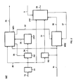
- FIG. 1 The general block diagram of the control circuit is shown in Fig. 1.
- connection 1 8-bit digital video signals reach through connection 1 a block INP, which is the video-flow decoder. It extracts synchronism and active data in each line, temporarily storing them in a buffer memory to obtain output flux synchronization, supplied on connection 2.
- connection 2 In addition to line and field synchronism and field parity code, on connection 2 there are output 16-bit video data in Y,Cb,Cr format.
- block INP receives control signals of the emission of video data.
- Connection 1 reaches also block MX2, a multiplexer allowing sending to output 5 the digital video flux present on connection 1 or the one present on connection 4, under the control of the signal on wire 6. In such a way it is sent to the output either the same input flux or the one generated inside the control circuit by block OUT.
- 16-bit video data in Y,Cb,Cr format arrive from the outside through connection 7, together with signals for controlling data input, i.e. enabling, clock, selection signals. They are led to block VID, which synchronises them using timings established from the outside and converts them into RGB format, making them available on connection 8 with a 24-bit parallelism, plus the clock signal. The same data are made available in Y,Cb,Cr format, still with 24 bit parallelism, on connection 21.
- connection 9 block VID carries out also the control of an external video memory, containing a secondary image superimposable to the current image named "overlay memory”. More particularly VID generates on connection 9 the addresses, and at varying instants, receives video data and synchronism signals.
- Timing signals needed by block VID, are sent from block TIM through connection 10.
- signals specifying pixel position whose value is sent onto connection 8, consisting of horizontal and vertical synchronism and of pixel clock.
- Block VID interfaces the control microprocessor through block INT and connections 11 and 12. Through connection 11 it receives from the microprocessor the commands for programming its registers and through connection 12 it allows the microprocessor to read its operating condition.
- block VID renders available to the outside vertical, horizontal and parity signals, as well as state signals, e.g. filling state of the buffer memory, and a control signal for an external video multiplexer, allowing the image present on connection 8 to be combined with an external video image.
- Block TIM generates the timing signals for the whole circuit, sending them both on the already examined connection 10, and on connection 14 towards block OUT.
- Block TIM receives from the outside the pixel clock and external horizontal and vertical synchronism signals through connection 15.
- Two connections 16 and 17 allow the external microprocessor to program and check the block operation respective!y.
- Block INT allows address signal decoding coming from the external microprocessor on connection 18, granting it the access to one of the internal registers.
- the datum to be written at the specified address is to be rendered available by the microprocessor on connection 19, at the input to block INT, which forwards it on connections 11 and 16.
- Connection 20 presents the address of the register the microprocessor wants to read to block MX1, a multiplexer which transfers to the output on connection 19 one of the data present on connections 12 or 17.
- block OUT converts 24-bit data under Y,Cb,Cr format, present on connection 21, into data under CCIR 656 format, it renders available on connection 4. Timings for the correct operation of OUT are supplied by block TIM through connection 14.
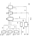
- Fig. 2 shows the block diagram denoted by INP on Fig.1, which operates video flow decoding.
- Digital video data and relevant timings are present on connections 1a and 1b respectively.
- Digital video data are first stored in a register R1 and then transferred into a register R3.
- connection 31 there is the first input datum and on connection 30 the second datum, which can now be taken as an only 16-bit datum and sent to block FIF.
- the frequency of data sent to FIF is equal to half that of the arriving data, which renders constraints on the performance of block FIF less stringent in terms of operating speed.
- Connection 30 reaches also a block MS1, consisting of a finite state automaton, which extracts synchronism information present in the digital data flow and renders them available on connection 2b. Besides it generates on connection 32 a signal indicating that the data present on connections 31 and 30 are significant to block FIF. Block MS1 is clocked by the signal present on connection 1b, at the same frequency of the arriving data.
- MS1 receives an enabling signal when a block CRP realizes that the information on video synchronism contains some errors.
- block CRP receives through connection 34 the code containing synchronism state and relative parity from a register R2.
- CRP effects the analysis of data and of their parity and is capable of correcting an error and signalling the presence of two errors. In the first case it sends the correct synchronism information to MS1, while in the second case blocks MS1 at the preceding state.
- Register R2 receives its timing signal from MS1 via a connection 35, so as to be able to extract at the suitable instant the synchronism word from the input data flow.
- Block FIF basically consisting of a FIFO memory, allows the input data frequency to be matched with the output data frequency. It is controlled by a finite-state automaton MS2 through connection 36, on which selection signals and writing pulses are transiting. To generate these signals, MS2 needs information on the validity of data supplied by MS1 on connection 32 and of the clock signal present on connection 1b. Besides block FIF communicates to MS2 on wire 37 the possible fullness of FIFO memory, by blocking further writing operations. Finally, FIF receives selection signals and pulses of data reading in the FIFO memory through connection 3, supplying them onto a 16-bit connection 2a.
- Fig.3 represents a block diagram of the block denoted by VID in Fig.1.
- connection 7a the 16-bit video data under the Y,Cb,Cr format, coming from an external video memory, enter the block and are inserted into a buffer memory of the FIFO type, denoted by FOF.
- FOF the FIFO type
- Block FOF reorganises data so as to present them at the 24-bit output 50. Timing signals controlling output data flow are generated by block SYN, which supplies them on connection 51.
- Block FOF signals to the outside of the circuit the emptiness state of FIFO memory by a signal sent onto connection 13b, so as to inform the external microprocessor of the necessity of sending new data.
- Block OVE controls the data routing inside the whole block VID on the basis of its programming, set by the external microprocessor, and also of the data coming from the external overlay memory on connection 9a.
- connection 9b On connection 9b it generates the addresses and control signals for the external memory and on wire 13a a signal for controlling an external video multiplexer, as previously already disclosed. It is given necessary timing by block SYN on connection 52.
- Block OVE contains at its inside registers controlling the operation of the external overlay memory and of the memories containing the look-up tables. Registers and memories are programmable by an external microprocessor through connection 11. On 24-bit connection 53 there is the output of the colour memory with three Y,Cb,Cr components per each pixel.
- the colour memory contains 16 possible colours, the one being used which is specified by the contents of the external overlay memory for that pixel. One of these colours is used as a code to signal the non-superposition of the overlay image.
- Block OVE decodes this particular code and as a consequence controls through wire 54 a multiplexer MX3, so that either Y,Cb,Cr code present on connection 53, or Y,Cb,Cr code arriving from block FOF, relevant to the main image, is transferred to the output 21.
- 24-wire connections 55 and 56 carry respectively the code under RGB format relevant to the overlay image element and the control signal for a multiplexer MX4, which transfers to its output 8 either the code or the one, still under RGB format, coming from block MAD onto 24-wire connection 57.
- connection 12 the external microprocessor reads block OVE state, i.e. the contents of the registers previously written and some test bits.
- Block SYN starting from timing signals coming on connection 10, generates timings for blocks FOF and OVE, phase shifted so as to ensure data coherence on connections 50 and 53 or on connections 57 and 55.
- the mixing is carried out by MX4
- the delay introduced by block MAD is to be taken into account for the phase shift.
- horizontal and vertical synchronism and field parity signals of the image outgoing on connection 8 are present on connection 13c.
- the choice of the type of phase shift to be applied to its outputs 51 and 52 is carried out on the basis of the information received on connection 11.
- Block MAD converts data under Y,Cb,Cr format, present on connection 21, into data under RGB format, and renders them available on connection 57.
- MAD consists of an arithmetic unit capable of carrying out the additions and multiplications necessary to the conversion.
- connection 58 Some intermediate results, which are rendered available on connection 58 for test purposes, can be led to output 8 through multiplexer MX4.
- MX4 multiplexer
- Fig.4 shows the block diagram of the block denoted by OUT in Fig.1.
- Y,Cb,Cr components of the pixel to be converted into CCIR 656 format are present at the input on connections 21a, 21b and 21c respectively.
- the three sets of 8-bit signals are stored in registers RX1,RX2, and RX3, which receive timing signals from block TIM (Fig. 1) through wire 14a.
- CCIR 656 flow is obtained by duly combining Y,Cb,Cr values present at outputs 60, 61, and 62 of registers RX1, RX2 and RX3 through a multiplexer MX5.
- the codes relevant to synchronism and parity information, present inside CCIR 656 flow are generated by a block COD, by which they are supplied onto 8-bit connection 63 on the basis of the synchronism signal state present on connection 14b.
- Multiplexer MX5 is controlled by connection 64 by a finite state automaton MS3, which generates also on connection 67 control signals for generation of the synchronism words of CCIR 656 flow.
- the synchronism sequence consists of a word formed by all ones, followed by two words formed by all zeros.
- MS3 sends suitable set and reset signals to a register RX5, on the basis of synchronism signals generated with a suitable phase shift by block TIM (Fig.1) on connection 14c.
- Clock signal at pixel frequency for automaton MS3 and registers RX4 and RX5 is present on connection 14d.
- This chain of registers transfers the data present at MX5 output on connection 65 to output connection 4, duly synchronised thanks to the delay operated by RX4 and RX5, which introduces also the synchronism words.
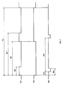
- Fig.5 shows the waveforms generated by block TIM (Fig.1) relevant to the horizontal timing.
- the waveform denoted by 10a which reference is equal to that of the wire whereupon it is present, is characterised by two time durations L and C.
- Value L represents the period of the waveform expressed in number of clock pulses and corresponds to the time duration of a line on the screen, whilst C, always expressed in number of clock pulses, represents the duration of the line blanking pulse.
- Waveform 10a still contains a pulse with the leading edge exactly positioned at the middle between the leading edges of the two adjacent pulses.
- This waveform is used as a clock signal by the vertical timing circuit.
- the waveform denoted by 10b as the wire on which it is present, has a period still equal to L and is characterised by two time durations D and W, which represent the delay of the trailing and leading edges with respect to the beginning of the period.
- Fig.6 shows the portion of the block TIM, denoted by TIMa, which generates the just described waveforms.
- Values L,C,D,W are contained in registers RLX,RCX,RDX and RWX, respectively; these registers, at the presence of a suitable signal on wire 16f, are loaded with initial values correspondent to standard TV format.
- Each individual register can be reached by the external microprocessor,which can change the initial values by modifying as a consequence the image format.
- the microprocessor presents data on connection 16e and, through enabling signals on wires 16a,16b,16c,16d, writes them in the four registers RCX,RLX,RDX,RWX. In case their contents are to be read, the microprocessor reaches the registers through connections 17a,17b,17e and 17f.
- 11-bit counter CN1 which counts at the pixel frequency the pulses present on wire 15b.
- the outputs of the counter on connection 70 are sent to a comparator CM1, which emits at its output 72 a signal indicating when counter CN1 output and the value present on connection 71 are equal.
- This value is supplied by one of the three high impedance driving circuits (Buffer tristate).
- Finite-state automaton MS4 is the circuit generating at its output the waveform 10a (Fig.5).
- MS4 enables through wire 73 buffer TR1,which as a consequence presents on connection 71, at the input of comparator CM1, the contents of register RCX, i.e. the value C of the waveform 10a (Fig.5).
- CM1 the contents of register RCX, i.e. the value C of the waveform 10a (Fig.5).
- MS4 receives on wire 72 the pulse signalling the equality found out 0 by CM1 and resets the signal on wire 10a, initially set to 1.
- a pulse of duration equal to C clock pulses is obtained.
- MS4 inhibits through wire 73 buffer TR1 and enables through wire 74 buffer TR2.
- the latter presents on connection 71 the value contained in RLX multiplied by 4.
- MS4 sets to 1 the signal on wire 10a and keeps it at 1 for two clock pulses.
- Buffer TR3 presents in turn on connection 71 the value contained in RLX multiplied by 8.
- MS4 sets to 1 the signal on wire 10a, enables through wire 76 counter CN1 to load the initial value supplied by multiplexer MX6 on connection 77, inhibits TR3 and re-enables TR1, to start a new cycle.
- connection 17c made available to the outside.
- the waveform on wire 10b is generated by a finite-state automaton MS5. It receives on wire 78 the pulses signalling the equality found out by a comparator CM2 between the value supplied by counter CN1 on connection 79 and the value supplied on connection 80 by a multiplexer MX7. The latter, controlled by a finite-state automaton MS6 through wire 81, presents alternately on connection 80 the values present on connections 17e and 17f, consisting of values contained in registers RDX and RWX respectively.
- connection 80 there is the value contained in RDX; when counter CN1 reaches such a value, MSS resets the signal on wire 10b. At the same time MS5 signals to MS6 through wire 82 its state change, that's why MS6 switches through wire 81 multiplexer MX7, which transfers onto connection 80 the contents of register RWX. When the counter CN1 reaches this new value, MS5 sets to 1 the signal on wire 10b, to start then a new cycle starting from the following line.
- the synchronization of the whole circuit TIMa with an external horizontal synchronism signal is carried out by finite-state automaton MS6.
- This automaton checks the phase relation existing between the external synchronism signal, present on wire 15a, and the synchronism signal generated by MS5 on wire 82. If the phase shift differs by a certain predetermined value, e.g. ⁇ 3 clock pulses, automaton MS6 operates resynchronization of the whole circuit by acting on MS4,MS5,CN1 by means of wires 83,84,85. In MS4 and MS5 it resets the outputs and in CN1 loads the value present on connection 77.
- a certain predetermined value e.g. ⁇ 3 clock pulses
- MS6 controls through wire 86 multiplexer MX6 so that it presents on connection 77 the signal at the output 87 of an adder AD1.
- the latter sums up to value D, present on connection 88, a constant value 0 N,present under wired form on connection 89.
- counter CN1 is loaded with value D+N, where N represents the intervention delay of automaton MS6.
- MS6 switches MX6 so as to cause the transfer on connection 77 of a constant value M, present under wired form on connection 90. This value represents the delay introduced by MS4 when it loads CN1 through wire 76.
- connection 17d made available to the outside.
- Fig.7 shows the waveforms generated by block TIM (Fig.1) relevant to the vertical timing.
- the waveform denoted by 10c which reference is equal to that of the wire whereupon it is present, is characterised by four time durations BP, FP,BD and FD, expressed in number of half-lines of TV frame.
- Value FD represents the waveform period and corresponds to time duration of a complete frame on the screen, while FP represents the duration of the even field.
- Value BD indicates the instants at which ends the retrace of the odd field and value BP represents the duration of retrace of the even field.
- the waveform denoted by 10d which reference is equal to that of the wire whereupon it is present, has a period always equal to FD and is characterised by three time durations DV,WV and SW,which represent respectively the delay of trailing edge, the delay of leading edge with respect to the beginning of the period and the interval between two subsequent trailing edges.
- This waveform is used as a vertical synchronism signal.
- the waveform denoted by 10e represents parity signal which identifies even and odd fields.
- Fig.8 shows the portion of the block TIM, denoted by TlMb, which generates the just described waveforms.
- Values BP,FP,BD and FD are contained in the block of registers RVX; these registers, at the presence of a suitable signal on wire 16f, are loaded with initial values correspondent to the standard TV format.
- Each individual register can be reached by the external microprocessor,which can change the initial values by modifying as a consequence the image format.
- RVY contains values DV,WV and SW. They also take up initial values under the control of the signal on wire 16f and can be written by the external microprocessor.
- the microprocessor presents data on connection 16e and, through enabling signals on connection 16g for RVX and 16h for RVY, writes them in the block of registers selected. In case their contents are to be read, the microprocessor reaches the registers through connections 17g and 17m.
- 11-bit counter CN2 which counts at halfline frequency, i.e. at a frequency twice as high as the line frequency, the pulses present on wire 10a.
- the outputs of the counter on connection 90 are sent to a comparator CM3, which emits at its output 92 a signal indicating when equality between the output of counter CN2 and the value present on connection 91 is reached.
- This value is supplied by a multiplexer MX9, addressed by finite state automaton MS7 through connection 93.
- Finite-state automaton MS7 is the circuit generating at its outputs waveforms 10c and 10e (Fig.7).
- MS7 enables through connection 93 multiplexer MX9, which as a consequence presents on connection 91, at the input of comparator CM3, the contents of register RVX, made available on connection 94, i.e. the value BP of the waveform 10c (Fig.7).
- MS7 receives on wire 92 the pulse signalling the equality found out by CM3 and resets the signal on wire 10c, initially set to 1.
- a pulse of duration equal to BP half-lines is obtained.
- MS7 switches through connection 93 multiplexer MX9, so as to present on connection 91 the value FP contained in RVX and present on connection 95.
- MS7 sets to 1 the signal on wire 10e, switches MX9 so that on connection 91 may appear signal BD, present on connection 96, and waits for the signalling of comparator CM3, indicating that this new value has been reached by CN2.
- MS7 resets to 0 the signal on wire 10c and switches MX9 so as it may present on connection 91 signal FD present on connection 97.
- the waveform on wire 10d is generated by a finite-state automaton MS8. It receives on wire 100 the pulses signalling the equality found out by a comparator CM4 between the value supplied by counter CN2 on connection 101 and the value supplied on connection 102 by a multiplexer M10. The latter, controlled by finite-state automaton MS8 through connection 103, presents alternately on connection 102 values DV and WV present on connections 104 and 105, or the same values summed up 5 to value SW present on connection 106.
- connection 102 there is value DV; when counter CN2 reaches such a value, MS8 resets the signal on wire 10d. At the same time MS8 signals to a finite-state automaton MS9 through wire 107 its state change and switches M10 so that it transfers on connection 102 value WV. When counter CN2 reaches this new value, MS8 sets again to 1 the signal on wire 10d and switches M10 so that it may present on connection 102 the sum of the values present on connections 104 and 106. Thus the pulse generation cycle of the signal on wire 10d is repeated, by using this time values DV plus SW and WV plus SW. At the end of the pulse value DV is presented again to comparator CM4 and the circuit is prepared for the subsequent frame.
- Finite-state automaton MS8 can be controlled during testing phase by the external microprocessor through connection 17i.
- the synchronization of the whole circuit TIMb with an external vertical synchronism signal is carried out by finite-state automaton MS9.
- This automaton checks the phase relation existing between the external synchronism signal, present on wire 15c, with the synchronism signal generated by MS8 on wire 107 MS9 counts the number of subsequent times wherein phase coincidence between the above-mentioned synchronism signals is lacking; when this number exceeds a certain predetermined value, automaton MS9 carries out resynchronization of the whole circuit acting on MS7 and MS8 through wires 108 and 109. In MS7 and MS8 it resets the outputs, which operation causes loading of the value present on connection 99 in CN2.
- MS9 controls through wire 110 multiplexer MX8 so that it may present on connection 99 the signal on connection 111, which represents value DV plus a constant value P, present under wired form in M10.
- connection 111 which represents value DV plus a constant value P
- counter CN2 is loaded with the value DV+P, wherein P represents intervention delay of automaton MS9.
- MS9 switches MX8 so as to cause the transfer on connection 99 of a constant value R, present under wired form on connection 112. This value represents the delay introduced by MS7 when it loads CN2 through wire 98.
- connection 17n made available to the outside.
- the just-described operation of the block TIMb refers to interlaced mode.
- the circuit can also operate in non-interlaced mode; the operation is analogous, but values FP,BD, and SW are no longer used.
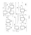
- Circuit MAD presented while describing fig.3, is represented in the block diagram of Fig.9.
- the Y,Cb,Cr components are presented at MAD input on connections 21c,21a,21b respectively and are stored in registers ZX3,ZX1,ZX2. From register ZX1 Cb component is sent to two read-only memories RO2 and RO4 through connections 151 and 150. Memory RO2 carries out multiplying operation of 256 values of Cb by 1,7381 and the subtraction of 222 from the results, using previously computed and permanently stored values. The result of the operations carried out by RC2 is led through connection 152 to a register ZX7,wherein it is stored and rendered available on connection 153 for an adder AD3.
- the other input of the adder receives through connection 154 the value Y,suitably delayed by the bank of registers ZX3,ZX4,ZX9 to take into account propagation delays through read-only-memory RO2.
- Y is then available the true value of B component.
- B is further delayed by a chain of registers Z11 and Z15, to take into account the propagation delays through an adder AD5, and is made available at the output on connection 156.
- Memory RO1 carries out the multiplication of 256 values of Cr by 1,36875 and subtraction of 175 from the results, using previously computed and permanently stored values.
- the result of the operations carried out by RO1 is led through connection 159 to a register ZX8,whereby it is stored and rendered available on connection 160 for an adder AD4.
- the other input of the adder receives through connection 154 the value Y,suitably delayed by the chain of registers ZX3,ZX4,ZX9 to take into account propagation delays through read-only memory RO1.
- the true value of R component is then available.
- R is further delayed by a chain of registers Z12 and Z16, to take into account the propagation delays through the adder AD5, and is made available at the output on connection 162.
- Cb and Cr components are read out from registers ZX1 and ZX2 through connections 150 and 157 and read-only memories RO3 and RO4 are addressed.
- the operations of multiplication of Cr by -0.6972 and addition 0 of 66 to the result take place in RO3, whilst the operations of multiplication of Cb by -0.33755 and addition of 66 to the result take place in RO4.
- Subdivision of additive coefficient into two parts allows simplification of read-only memories RO3 and RO4.
- G is stored in register Z14 and rendered available at the output on connection 171.
- connections 58a and 58b are rendered available to the outside.
- Fig. 10 shows the block diagram of the block denoted by OVE in Fig.3.
- the main task of this circuit is the generation of control signals of external overlay A memory. Besides it receives the overlay memory data and interprets them suitable.
- a counter denoted by CN3 generates the addresses for the overlay memory. This counter receives clock pulses at half-line frequency on connection 52 coming from block SYN (Fig.3).
- the counter can be loaded through connection 200 with the contents of register R23, containing starting-line value used while scanning the overlay memory.
- the external microprocessor can write in this register through connection 11 and read its contents through connection 12b.
- Register R22 contains instead the starting column used for scanning the overlay memory. Also in this register the external microprocessor can write through connection 11 and read the contents through connection 12a.
- the value of starting column is led through connection 201 to a multiplexer M21, whilst the other input receives on connection 202 the output of counter CN3.
- a register R20 stores the 8-bit value coming from the overlay memory on connection 9a.
- a subsequent multiplexer M20 alternately transfers to connection 203 the upper or lower part of this value, present on connections 204 and 205.
- the values of the new 4-bit format are sent to a conversion table LUT, which supplies at the output on connection 204 a 24-bit value per each of the 16 input values. 24-bit values, relevant to pixels, are programmable by the external microprocessor through connection 11.
- connection 204 The values on connection 204 are stored in register R21 and rendered available on connections 53 and 55 directed to multiplexers MX4 and MX3 (Fig.3).
- Connection 203 is also led to a block LOG, which generates control signals of the above-mentioned multiplexers on connections 54 and 56. It generates also on wire 13a the control signal for the external multiplexer already mentioned.
Landscapes
- Engineering & Computer Science (AREA)
- Multimedia (AREA)
- Signal Processing (AREA)
- General Engineering & Computer Science (AREA)
- Controls And Circuits For Display Device (AREA)
- Processing Of Color Television Signals (AREA)
- Editing Of Facsimile Originals (AREA)
- Color Image Communication Systems (AREA)
- Color Television Systems (AREA)
- Two-Way Televisions, Distribution Of Moving Picture Or The Like (AREA)
- Communication Control (AREA)
Description
- The present invention concerns apparatus for building up multimedia user terminals to be used in the Integrated Service Digital Network (ISDN) and more particularly a video control circuit for multimedia applications. The invention relates to such a video control circuit which has first input and a first output for digital video signals according to CCIR 656 recommendation, comprising the video data and control signals, a second input and a second output for video signals under luminance-chrominance Y,Cb,Cr format, also comprising video data and control signals, a third, alternative input/output for a connection to an external overlay video memory, a fourth input and a fourth output for a connection to an external control microprocessor, a fifth input for clock and synchronism signals and a fifth output for standard RGB signals.
- It is well known that in the development of the ISDN network, besides the usual telephone speech and data transmission services, the idea is of offering, in a capillary way to the home subscribers, additional telematic services, among which reception and transmission of documents by Group 4 facsimile equipment and reception and transmission of photo images at CCIR standard resolution.
- The Group 4 facsimile is real time transmission method of texts and images, sent onto the ISDN network with a particular coding and a 64 kbit/s rate, in which the whole process, from the composition moment (acquisition through a scanner, acquisition from the memory of a processor, etc.) up to the reception and printing, is of digital type. Noise immunity is very high and resolution is of 400 pixels per inch, higher than that of the analog facsimile presently used.
- There is also the possibility of transmitting photo images, locally obtained with a TV camera, residing in the memory of a processor or received from a distant data bank. Their resolution is that as from studio, foreseen in CCIR 656 recommendation, so they are to be displayed with suitable means in order to obtain good quality images with the same transmission resolution. This type of transmission can be used in the most different fields, e.g. it can meet the requirements of estate agents, tour operators, and the like, who could consult centralised data bases regrouping the offers available on the market at that moment. It could resolve the problem of the creation of a general archive of the works of art, facilitating the transmission of the images of paintings, monuments and others to the culture ministry and hence their vision by the public.
- To be able to access in a capillary way all these services, offered within an ISDN network, the subscribers must be equipped with suitable terminals capable of allowing the transmission, the reception, the display and possibly the printing of the exchanged documents. The costs of such terminals can be reduced by the use of the computer which is already widespread in private houses. With the addition of a suitable circuit and a suitable programme, it can become the first and more versatile terminal of the ISDN network.
- The circuit, which can be housed on one or more printed circuit boards, will permit the computer to carry out complex processing operations of the video signal in real time. It must comprise a video signal memory to be used for image acquisition from a TV camera or for display of images residing in the personal computer itself. Besides it must be equipped with interface circuits towards the digital ISDN network. A suitable circuit allowing the computer monitor, operating with its particular TV standard, to display the images with the characteristics specified in CCIR 656 recommendation, is also to be provided. Thus resorting to a specific monitor only for displaying the images with the specified characteristics is avoided.
- The control programme can be permanently stored under firmware format. To date it does not exist on the market a video control circuit capable of carrying out all the operations carried out by the circuit provided by the invention. It exists on the contrary a series of devices for carrying out some partial functions. They are generally dedicated to the processing of images and particularly to the graphics, and are used in the video control units installed in personal computers and workstations dedicated to CAD processes.
- E.g. there are programmable integrated circuits, named "Colour video controller", such as those identified by IMS G300B and described on
page 87 and ff. of the catalogue 1990 of INMOS, which implement the real-time control functions of a graphic system and of its display means, e.g. a cathode ray tube (CRT), a laser printer or a colour plotter. They can be interfaced with the bus of each standard processor, wherefrom they receive the programmes necessary to specify timings and data display characteristics on the screen of the CRT or on a printed sheet. They can also be interfaced with the source of data to be represented, using in both cases dual-port memories which allow speed up the procedures to the maximum. Said controllers contain a video timing generator, completely programmable by the external microprocessor, which generates video synchronism, addresses, data timing and all the display characteristics required, such as: image dimension, vertical and horizontal scanning frequency, presence of interlacing, etc. They contain in addition three totally-programmable memories, the so called "colour look-up tables", allowing the representation of output data with a certain number of colours chosen out of a larger set.The three RGB flows outgoing from the table are converted into analog form to be directly sent to the video screen. - Moreover, there is another type of integrated circuits, such as those identified by IMS G178, described on
page 63 and ff. of the above catalogue 1990 of INMOS, which implement the already-described "Colour look-up table" function, i.e. the storing of the colour values to be associated to different screen points. They comprise three biport memories, generally of small capacity, each relative to one of the primary colours processed (RGB = red, green, blue). Each memory is loaded and the contents is updated by the microprocessor controlling the system. The reading of the memories is carried out by using instantaneous values of RGB data flow to be displayed as addresses, each of them corresponding to a suitable value which is presented at the output gate. The three values obtained thus, converted into analog form, form the tern determining the colour of a pixel of the screen. - As mentioned, said integrated circuits are particularly oriented towards graphic applications in personal computer and workstations, by implementing the typical specifications of graphic cards, such as VGA, EGA, etc. Besides they are apt to process the signals under the format of the fundamental RGB colours, while CCIR standards require the photographic images be processed under the format of luminance and chrominance components.
- The limitations above are eliminated by the video control circuit for multimedia applications provided by the present invention, which is capable of processing both photographic and graphic video images, by satisfying both the relevant CCIR standards, and the specifications proper to personal computers, VGA, EGA, etc, so as to allow the representation of the two types of images on an only type of display. To this aim, it is capable of generating both the timings proper to the CCIR standards for a resolution of 720 columns per 576 lines, and the timings proper to VGA specification, for a resolution of 640 columns per 480 lines, with an upper representation limit of graphic planes of 1024 columns per 1024 lines.
- It is the main object of the present invention a video control circuit for multimedia applications, such as described in claim 1.
- The foregoing and other characteristics of the present invention will be made clearer by the following description of a preferred embodiment thereof, given by way of non limiting example, and by the annexed drawing, wherein:
- Fig.1 is the general block diagram of the control circuit;
- Fig.2 is the block diagram of the block denoted by INP in Fig.1;
- Fig.3 is the block diagram of the block denoted by VID in Fig.1;
- Fig.4 is the block diagram of the block denoted by OUT in Fig.1;
- Fig 5 is a time diagram relevant to horizontal timing generated by block TIM of Fig.1;
- Fig.6 is the block diagram of part TlMa of the block denoted by TIM in Fig.1;
- Fig.7 is a time diagram relevant to vertical timing generated by block TIM of Fig.1;
- Fig.8 is the block diagram of the portion TIMb of the block denoted by TIM in Fig.1;
- Fig.9 is the block diagram of the block denoted by MAD in Fig.3;
- Fig. 10 is the block diagram of the block denoted by OVE in Fig.3.
- The video control circuit accepts at the input a digital video signal according to CCIR 656 recommendation and renders it available at the output still in digital form with 16 bit parallelism and with separated synchronism signals.
- Besides it accepts at the input a digital video signal in luminance-chrominance format (Y,Cb,Cr), mixes it with another 8 bit video signal and converts it into a standard RGB signal for colour monitor.
- The same RGB output is converted into a digital video signal according to CCIR 656 recommendation.
- Programming the image format from the outside is possible: number of lines per each field, number of pixels per each line, operation in interlaced or non-interlaced mode.
- The whole timing can be synchronised by signals supplied from the outside and all the functions can be programmed from the outside by a microprocessor.
- The general block diagram of the control circuit is shown in Fig. 1.
- 8-bit digital video signals reach through
connection 1 a block INP, which is the video-flow decoder. It extracts synchronism and active data in each line, temporarily storing them in a buffer memory to obtain output flux synchronization, supplied onconnection 2. In addition to line and field synchronism and field parity code, onconnection 2 there are output 16-bit video data in Y,Cb,Cr format. Onconnection 3 block INP receives control signals of the emission of video data.Connection 1 reaches also block MX2, a multiplexer allowing sending to output 5 the digital video flux present on connection 1 or the one present on connection 4, under the control of the signal onwire 6. In such a way it is sent to the output either the same input flux or the one generated inside the control circuit by block OUT. - 16-bit video data in Y,Cb,Cr format arrive from the outside through
connection 7, together with signals for controlling data input, i.e. enabling, clock, selection signals. They are led to block VID, which synchronises them using timings established from the outside and converts them into RGB format, making them available onconnection 8 with a 24-bit parallelism, plus the clock signal. The same data are made available in Y,Cb,Cr format, still with 24 bit parallelism, onconnection 21. - Through
connection 9 block VID carries out also the control of an external video memory, containing a secondary image superimposable to the current image named "overlay memory". More particularly VID generates onconnection 9 the addresses, and at varying instants, receives video data and synchronism signals. - All the timing signals, needed by block VID, are sent from block TIM through
connection 10. Among them there are the signals specifying pixel position, whose value is sent ontoconnection 8, consisting of horizontal and vertical synchronism and of pixel clock. - Block VID interfaces the control microprocessor through block INT and
connections connection 11 it receives from the microprocessor the commands for programming its registers and throughconnection 12 it allows the microprocessor to read its operating condition. - Finally, through
connection 13, block VID renders available to the outside vertical, horizontal and parity signals, as well as state signals, e.g. filling state of the buffer memory, and a control signal for an external video multiplexer, allowing the image present onconnection 8 to be combined with an external video image. - Block TIM generates the timing signals for the whole circuit, sending them both on the already examined
connection 10, and onconnection 14 towards block OUT. Block TIM receives from the outside the pixel clock and external horizontal and vertical synchronism signals throughconnection 15. Twoconnections - Block INT allows address signal decoding coming from the external microprocessor on
connection 18, granting it the access to one of the internal registers. The datum to be written at the specified address is to be rendered available by the microprocessor onconnection 19, at the input to block INT, which forwards it onconnections Connection 20 presents the address of the register the microprocessor wants to read to block MX1, a multiplexer which transfers to the output onconnection 19 one of the data present onconnections - Finally, block OUT converts 24-bit data under Y,Cb,Cr format, present on
connection 21, into data under CCIR 656 format, it renders available on connection 4. Timings for the correct operation of OUT are supplied by block TIM throughconnection 14. - Fig. 2 shows the block diagram denoted by INP on Fig.1, which operates video flow decoding.
- Digital video data and relevant timings are present on
connections - As a result of the storing and of transferring, on
connection 31 there is the first input datum and onconnection 30 the second datum, which can now be taken as an only 16-bit datum and sent to block FIF. Thanks to parallelism doubling, the frequency of data sent to FIF is equal to half that of the arriving data, which renders constraints on the performance of block FIF less stringent in terms of operating speed. -
Connection 30 reaches also a block MS1, consisting of a finite state automaton, which extracts synchronism information present in the digital data flow and renders them available onconnection 2b. Besides it generates on connection 32 a signal indicating that the data present onconnections connection 1b, at the same frequency of the arriving data. - Through
wire 33, MS1 receives an enabling signal when a block CRP realizes that the information on video synchronism contains some errors. In fact block CRP receives throughconnection 34 the code containing synchronism state and relative parity from a register R2. CRP effects the analysis of data and of their parity and is capable of correcting an error and signalling the presence of two errors. In the first case it sends the correct synchronism information to MS1, while in the second case blocks MS1 at the preceding state. Register R2 receives its timing signal from MS1 via aconnection 35, so as to be able to extract at the suitable instant the synchronism word from the input data flow. - Block FIF, basically consisting of a FIFO memory, allows the input data frequency to be matched with the output data frequency. It is controlled by a finite-state automaton MS2 through
connection 36, on which selection signals and writing pulses are transiting. To generate these signals, MS2 needs information on the validity of data supplied by MS1 onconnection 32 and of the clock signal present onconnection 1b. Besides block FIF communicates to MS2 onwire 37 the possible fullness of FIFO memory, by blocking further writing operations. Finally, FIF receives selection signals and pulses of data reading in the FIFO memory throughconnection 3, supplying them onto a 16-bit connection 2a. - Fig.3 represents a block diagram of the block denoted by VID in Fig.1. Through
connection 7a the 16-bit video data under the Y,Cb,Cr format, coming from an external video memory, enter the block and are inserted into a buffer memory of the FIFO type, denoted by FOF. The timing relevant to the writing of these data, enabling, clock, selection, arrives on the contrary through 3-wire connection 7b. - Block FOF reorganises data so as to present them at the 24-
bit output 50. Timing signals controlling output data flow are generated by block SYN, which supplies them onconnection 51. - Block FOF signals to the outside of the circuit the emptiness state of FIFO memory by a signal sent onto
connection 13b, so as to inform the external microprocessor of the necessity of sending new data. - Block OVE controls the data routing inside the whole block VID on the basis of its programming, set by the external microprocessor, and also of the data coming from the external overlay memory on
connection 9a. Onconnection 9b it generates the addresses and control signals for the external memory and onwire 13a a signal for controlling an external video multiplexer, as previously already disclosed. It is given necessary timing by block SYN onconnection 52. - Block OVE contains at its inside registers controlling the operation of the external overlay memory and of the memories containing the look-up tables. Registers and memories are programmable by an external microprocessor through
connection 11. On 24-bit connection 53 there is the output of the colour memory with three Y,Cb,Cr components per each pixel. The colour memory contains 16 possible colours, the one being used which is specified by the contents of the external overlay memory for that pixel. One of these colours is used as a code to signal the non-superposition of the overlay image. Block OVE decodes this particular code and as a consequence controls through wire 54 a multiplexer MX3, so that either Y,Cb,Cr code present onconnection 53, or Y,Cb,Cr code arriving from block FOF, relevant to the main image, is transferred to theoutput 21. - Analogously, 24-
wire connections output 8 either the code or the one, still under RGB format, coming from block MAD onto 24-wire connection 57. - Through
connection 12 the external microprocessor reads block OVE state, i.e. the contents of the registers previously written and some test bits. - Block SYN, starting from timing signals coming on
connection 10, generates timings for blocks FOF and OVE, phase shifted so as to ensure data coherence onconnections connections connection 8 are present onconnection 13c. The choice of the type of phase shift to be applied to itsoutputs connection 11. - Block MAD converts data under Y,Cb,Cr format, present on
connection 21, into data under RGB format, and renders them available onconnection 57. MAD consists of an arithmetic unit capable of carrying out the additions and multiplications necessary to the conversion. - Some intermediate results, which are rendered available on
connection 58 for test purposes, can be led tooutput 8 through multiplexer MX4.The latter besides mixing signals onconnections connection 8 the signals onconnections - Fig.4 shows the block diagram of the block denoted by OUT in Fig.1. Y,Cb,Cr components of the pixel to be converted into CCIR 656 format are present at the input on
connections wire 14a. CCIR 656 flow is obtained by duly combining Y,Cb,Cr values present atoutputs bit connection 63 on the basis of the synchronism signal state present onconnection 14b. - Multiplexer MX5 is controlled by
connection 64 by a finite state automaton MS3, which generates also onconnection 67 control signals for generation of the synchronism words of CCIR 656 flow. The synchronism sequence consists of a word formed by all ones, followed by two words formed by all zeros. To obtain that, MS3 sends suitable set and reset signals to a register RX5, on the basis of synchronism signals generated with a suitable phase shift by block TIM (Fig.1) onconnection 14c. Clock signal at pixel frequency for automaton MS3 and registers RX4 and RX5 is present onconnection 14d. This chain of registers transfers the data present at MX5 output onconnection 65 to output connection 4, duly synchronised thanks to the delay operated by RX4 and RX5, which introduces also the synchronism words. - Fig.5 shows the waveforms generated by block TIM (Fig.1) relevant to the horizontal timing.
- The waveform denoted by 10a, which reference is equal to that of the wire whereupon it is present, is characterised by two time durations L and C. Value L represents the period of the waveform expressed in number of clock pulses and corresponds to the time duration of a line on the screen, whilst C, always expressed in number of clock pulses, represents the duration of the line blanking pulse.
Waveform 10a still contains a pulse with the leading edge exactly positioned at the middle between the leading edges of the two adjacent pulses. - This waveform is used as a clock signal by the vertical timing circuit.
- The waveform denoted by 10b, as the wire on which it is present, has a period still equal to L and is characterised by two time durations D and W, which represent the delay of the trailing and leading edges with respect to the beginning of the period.
- These waveforms are used as horizontal synchronism signals.
- Fig.6 shows the portion of the block TIM, denoted by TIMa, which generates the just described waveforms. Values L,C,D,W are contained in registers RLX,RCX,RDX and RWX, respectively; these registers, at the presence of a suitable signal on
wire 16f, are loaded with initial values correspondent to standard TV format. - Each individual register can be reached by the external microprocessor,which can change the initial values by modifying as a consequence the image format. The microprocessor presents data on connection 16e and, through enabling signals on
wires connections - An important function is carried out by 11-bit counter CN1, which counts at the pixel frequency the pulses present on
wire 15b. The outputs of the counter onconnection 70 are sent to a comparator CM1, which emits at its output 72 a signal indicating when counter CN1 output and the value present onconnection 71 are equal. This value is supplied by one of the three high impedance driving circuits (Buffer tristate). TR1, TR2, TR3, enabled in turn by finite-state automaton MS4 throughwires - Finite-state automaton MS4 is the circuit generating at its output the
waveform 10a (Fig.5). At the beginning MS4 enables throughwire 73 buffer TR1,which as a consequence presents onconnection 71, at the input of comparator CM1, the contents of register RCX, i.e. the value C of thewaveform 10a (Fig.5). When the counting value of CN1 reaches C, MS4 receives onwire 72 the pulse signalling the equality found out 0 by CM1 and resets the signal onwire 10a, initially set to 1. Thus a pulse of duration equal to C clock pulses is obtained. - At this instant, MS4 inhibits through
wire 73 buffer TR1 and enables throughwire 74 buffer TR2. The latter presents onconnection 71 the value contained in RLX multiplied by 4. When counter CN1 reaches this value, MS4 sets to 1 the signal onwire 10a and keeps it at 1 for two clock pulses. - Meanwhile, TR2 is inhibited and TR3 is enabled through
wire 75. Buffer TR3 presents in turn onconnection 71 the value contained in RLX multiplied by 8. When CN1 reaches this value, which represents the duration of a horizontal line in number of clock pulses, MS4 sets to 1 the signal onwire 10a, enables throughwire 76 counter CN1 to load the initial value supplied by multiplexer MX6 onconnection 77, inhibits TR3 and re-enables TR1, to start a new cycle. - During the testing phase, it is possible to observe the operation of finite-state automaton MS4 through
connection 17c, made available to the outside. - The waveform on
wire 10b is generated by a finite-state automaton MS5. It receives onwire 78 the pulses signalling the equality found out by a comparator CM2 between the value supplied by counter CN1 onconnection 79 and the value supplied onconnection 80 by a multiplexer MX7. The latter, controlled by a finite-state automaton MS6 throughwire 81, presents alternately onconnection 80 the values present onconnections - At first on
connection 80 there is the value contained in RDX; when counter CN1 reaches such a value, MSS resets the signal onwire 10b. At the same time MS5 signals to MS6 throughwire 82 its state change, that's why MS6 switches throughwire 81 multiplexer MX7, which transfers ontoconnection 80 the contents of register RWX. When the counter CN1 reaches this new value, MS5 sets to 1 the signal onwire 10b, to start then a new cycle starting from the following line. - The synchronization of the whole circuit TIMa with an external horizontal synchronism signal is carried out by finite-state automaton MS6. This automaton checks the phase relation existing between the external synchronism signal, present on
wire 15a, and the synchronism signal generated by MS5 onwire 82. If the phase shift differs by a certain predetermined value, e.g. ± 3 clock pulses, automaton MS6 operates resynchronization of the whole circuit by acting on MS4,MS5,CN1 by means ofwires connection 77. In case of resynchronization, MS6 controls throughwire 86 multiplexer MX6 so that it presents onconnection 77 the signal at theoutput 87 of an adder AD1. The latter sums up to value D, present onconnection 88, a constant value 0 N,present under wired form onconnection 89. In this way, counter CN1 is loaded with value D+N, where N represents the intervention delay of automaton MS6. - Once the synchronism is attained, MS6 switches MX6 so as to cause the transfer on
connection 77 of a constant value M, present under wired form onconnection 90. This value represents the delay introduced by MS4 when it loads CN1 throughwire 76. - 5 During the testing phase, it is possible to observe the operation of finite-state automaton MS6 through
connection 17d, made available to the outside. - Fig.7 shows the waveforms generated by block TIM (Fig.1) relevant to the vertical timing.
- The waveform denoted by 10c, which reference is equal to that of the wire whereupon it is present, is characterised by four time durations BP, FP,BD and FD, expressed in number of half-lines of TV frame. Value FD represents the waveform period and corresponds to time duration of a complete frame on the screen, while FP represents the duration of the even field. Value BD indicates the instants at which ends the retrace of the odd field and value BP represents the duration of retrace of the even field.
- The waveform denoted by 10d, which reference is equal to that of the wire whereupon it is present, has a period always equal to FD and is characterised by three time durations DV,WV and SW,which represent respectively the delay of trailing edge, the delay of leading edge with respect to the beginning of the period and the interval between two subsequent trailing edges. This waveform is used as a vertical synchronism signal.
- The waveform denoted by 10e represents parity signal which identifies even and odd fields.
- Fig.8 shows the portion of the block TIM, denoted by TlMb, which generates the just described waveforms. Values BP,FP,BD and FD are contained in the block of registers RVX; these registers, at the presence of a suitable signal on
wire 16f, are loaded with initial values correspondent to the standard TV format. - Each individual register can be reached by the external microprocessor,which can change the initial values by modifying as a consequence the image format.
- Another group of registers RVY contains values DV,WV and SW. They also take up initial values under the control of the signal on
wire 16f and can be written by the external microprocessor. - The microprocessor presents data on connection 16e and, through enabling signals on
connection 16g for RVX and 16h for RVY, writes them in the block of registers selected. In case their contents are to be read, the microprocessor reaches the registers throughconnections - An important function is carried out by 11-bit counter CN2, which counts at halfline frequency, i.e. at a frequency twice as high as the line frequency, the pulses present on
wire 10a. The outputs of the counter onconnection 90 are sent to a comparator CM3, which emits at its output 92 a signal indicating when equality between the output of counter CN2 and the value present onconnection 91 is reached. This value is supplied by a multiplexer MX9, addressed by finite state automaton MS7 throughconnection 93. - Finite-state automaton MS7 is the circuit generating at its
outputs waveforms connection 93 multiplexer MX9, which as a consequence presents onconnection 91, at the input of comparator CM3, the contents of register RVX, made available onconnection 94, i.e. the value BP of thewaveform 10c (Fig.7). When the counting value of CN2 reaches BP, MS7 receives onwire 92 the pulse signalling the equality found out by CM3 and resets the signal onwire 10c, initially set to 1. Thus, a pulse of duration equal to BP half-lines is obtained. - At this instant, MS7 switches through
connection 93 multiplexer MX9, so as to present onconnection 91 the value FP contained in RVX and present onconnection 95. When counter CN2 reaches this value, MS7 sets to 1 the signal onwire 10e, switches MX9 so that onconnection 91 may appear signal BD, present onconnection 96, and waits for the signalling of comparator CM3, indicating that this new value has been reached by CN2. Hence MS7 resets to 0 the signal onwire 10c and switches MX9 so as it may present onconnection 91 signal FD present onconnection 97. - When CN2 reaches this value, which represents the duration of a frame in number of half-lines, MS7 sets again to 1 the signal on
wire 10c. Besides it enables throughwire 98 counter CN2 to load the initial value supplied by multiplexer MX8 onconnection 99 and switches again MX9 to start a new cycle.During the testing phase, it is possible to observe the operation of finite-state automaton MS7 throughconnection 17h, made available to the outside. - The waveform on
wire 10d is generated by a finite-state automaton MS8. It receives onwire 100 the pulses signalling the equality found out by a comparator CM4 between the value supplied by counter CN2 onconnection 101 and the value supplied onconnection 102 by a multiplexer M10. The latter, controlled by finite-state automaton MS8 throughconnection 103, presents alternately onconnection 102 values DV and WV present onconnections connection 106. - At first on
connection 102 there is value DV; when counter CN2 reaches such a value, MS8 resets the signal onwire 10d. At the same time MS8 signals to a finite-state automaton MS9 throughwire 107 its state change and switches M10 so that it transfers onconnection 102 value WV. When counter CN2 reaches this new value, MS8 sets again to 1 the signal onwire 10d and switches M10 so that it may present onconnection 102 the sum of the values present onconnections wire 10d is repeated, by using this time values DV plus SW and WV plus SW. At the end of the pulse value DV is presented again to comparator CM4 and the circuit is prepared for the subsequent frame. - Finite-state automaton MS8 can be controlled during testing phase by the external microprocessor through
connection 17i. - The synchronization of the whole circuit TIMb with an external vertical synchronism signal is carried out by finite-state automaton MS9. This automaton checks the phase relation existing between the external synchronism signal, present on
wire 15c, with the synchronism signal generated by MS8 onwire 107 MS9 counts the number of subsequent times wherein phase coincidence between the above-mentioned synchronism signals is lacking; when this number exceeds a certain predetermined value, automaton MS9 carries out resynchronization of the whole circuit acting on MS7 and MS8 throughwires connection 99 in CN2. In case of resynchronization, MS9 controls throughwire 110 multiplexer MX8 so that it may present onconnection 99 the signal onconnection 111, which represents value DV plus a constant value P, present under wired form in M10. In this way, counter CN2 is loaded with the value DV+P, wherein P represents intervention delay of automaton MS9. - Once the synchronism has been attained, MS9 switches MX8 so as to cause the transfer on
connection 99 of a constant value R, present under wired form onconnection 112. This value represents the delay introduced by MS7 when it loads CN2 throughwire 98. - During the testing phase, it is possible to observe the operation of finite-state automaton MS9 through
connection 17n, made available to the outside. The just-described operation of the block TIMb refers to interlaced mode. The circuit can also operate in non-interlaced mode; the operation is analogous, but values FP,BD, and SW are no longer used. - Circuit MAD, presented while describing fig.3, is represented in the block diagram of Fig.9.
- It operates the conversion from Y,Cb,Cr format into RGB format. As known, the three R,G,B components can be expressed in comparison with Y,Cb,Cr components by the following formulae:


- The Y,Cb,Cr components are presented at MAD input on
connections connections connection 152 to a register ZX7,wherein it is stored and rendered available onconnection 153 for an adder AD3. The other input of the adder receives throughconnection 154 the value Y,suitably delayed by the bank of registers ZX3,ZX4,ZX9 to take into account propagation delays through read-only-memory RO2. At the output of AD3, onconnection 58a, is then available the true value of B component. B is further delayed by a chain of registers Z11 and Z15, to take into account the propagation delays through an adder AD5, and is made available at the output onconnection 156. - Analogously for the generation of R component, from register ZX2 the Cr component is sent to two read-only memories RO3 and RO1 through
connections connection 159 to a register ZX8,whereby it is stored and rendered available onconnection 160 for an adder AD4. The other input of the adder receives throughconnection 154 the value Y,suitably delayed by the chain of registers ZX3,ZX4,ZX9 to take into account propagation delays through read-only memory RO1. At the output of AD4, onconnection 58b, the true value of R component is then available. R is further delayed by a chain of registers Z12 and Z16, to take into account the propagation delays through the adder AD5, and is made available at the output onconnection 162. - As to generation of G component, Cb and Cr components are read out from registers ZX1 and ZX2 through
connections - The results of the operations carried out by RO3 and RO4 are led through
connections connections connection 167, is stored in register Z10 and throughconnection 168 is led to adder AD5. The other input of the adder receives throughconnection 169 the value Y, previously delayed in the chain of registers ZX3,ZX4, ZX9 and Z13, to take into account propagation delays through read-only memories RO3, RO4 and adder AD2. - At the output of AD5, on
connection 170, the true value of G component is then available. G is stored in register Z14 and rendered available at the output onconnection 171. - To facilitate the testing phase of memories RO1 and RO2,
connections - Fig. 10 shows the block diagram of the block denoted by OVE in Fig.3. The main task of this circuit is the generation of control signals of external overlay A memory. Besides it receives the overlay memory data and interprets them suitable. A counter denoted by CN3 generates the addresses for the overlay memory. This counter receives clock pulses at half-line frequency on
connection 52 coming from block SYN (Fig.3). The counter can be loaded throughconnection 200 with the contents of register R23, containing starting-line value used while scanning the overlay memory. The external microprocessor can write in this register throughconnection 11 and read its contents throughconnection 12b. Register R22 contains instead the starting column used for scanning the overlay memory. Also in this register the external microprocessor can write throughconnection 11 and read the contents throughconnection 12a. - The value of starting column is led through
connection 201 to a multiplexer M21, whilst the other input receives onconnection 202 the output of counter CN3. At the output of the multiplexer onconnection 9b there are then present alternately the line or column address of the overlay memory, in function of the control signals onconnection 9c. A register R20 stores the 8-bit value coming from the overlay memory onconnection 9a. A subsequent multiplexer M20 alternately transfers toconnection 203 the upper or lower part of this value, present onconnections connection 11. - The values on
connection 204 are stored in register R21 and rendered available onconnections Connection 203 is also led to a block LOG, which generates control signals of the above-mentioned multiplexers onconnections wire 13a the control signal for the external multiplexer already mentioned. - It is clear that what described is given by way of a non limiting example. Variations and modifications are possible without going out of the scope of the claims.
Claims (8)
- A video control circuit for multimedia applications, having a first input (1) and a first output (5) for digital video signals according to CCIR 656 recommendation, comprising the video data and control signals, a second input (7) and a second output (2) for video signals under luminance-chrominance Y,Cb,Cr format, also comprising video data and control signals, a third, alternative input/output (9) for a connection to an external overlay video memory, a fourth input (18) and a fourth output (19) for a connection to an external control microprocessor, a fifth input (15) for clock and synchronism signals and a fifth output (8) for standard RGB signals, the control circuit comprising:- a video flow decoder (INP), adapted to receive at the first input (1) the digital video signals according to CCIR 656, to extract synchronism signals and active data from these video signals and to store the active data in a buffer memory adapted to supply an outgoing flow, synchronized by the synchronism signals and supplied under Y,Cb,Cr format, at the second output (2);- a block (VID), adapted to receive at the second input (7) of the control circuit the video data under Y,Cb,Cr format together with its control signals, to synchronize these video data using timings determined from the outside, to vary their parallelism and to convert them into RGB format, supplying the resulting signal to a first output (8) of the block (VID), the first output (8) of the block being the fifth output (8) of the control circuit, while supplying Y,Cb,Cr signals at a second output (21), besides it is adapted to control the external overlay video memory containing a secondary image superimposable to the current image, and to supply (13) synchronism and state signals extracted from the input video signals under Y,Cb,Cr format;- a conversion block (OUT), adapted to convert the data on the second output (21) of the block (VID) which are in Y,Cb,Cr format (21) into data in CCIR 656 format;- a first multiplexer (MX2), adapted to transfer to the first output (5) of the control circuit a digital video signal present at the first input (1) of the control circuit or the signal from the output (4) of the conversion block (OUT);- a timing signal generator (TIM), programmable (16) via said fourth input (18) for the connection to the external control microprocessor;- an interface (INT), adapted for the dialogue of said block (VID) with the external control microprocessor;- a second multiplexer (MX1), adapted to transfer to the fourth output (19) of the control circuit the data coming either from the timing signal generator (TIM) or from said block (VID).
- A video control circuit for multimedia applications as in claim 1, characterized in that said video flow decoder (INP) comprises:- two registers (R1,R3) which are adapted that therein the digital video data from the first input (1) and the relevant timings are stored with a certain parallelism and read with a higher parallelism;- a frequency conversion block (FIF), basically consisting of a FIFO memory, adapted to store the digital data supplied by said registers (R1,R3);- a first finite-state automaton (MS1), adapted to extract the synchronism information present in the digital data from the first input (1), to render them available at the second output (2b) of the control circuit and to check data validity;- a block for detecting synchronism errors (CRP), adapted to analyse data and their parity and to correct an error or to signal the presence of two of them to said finite-state automaton (MS1);- a register (R2) adapted for storing the synchronism state and the relevant parity to send them to the block for detecting synchronism errors (CRP);- a second finite-state automaton (MS2), adapted for controlling said frequency conversion block (FIF) on the basis of the information on the data validity and of clock signals.
- A video control circuit for multimedia applications as in claim 1 or 2, characterized in that said block (VID) comprises:- a buffer memory of FIFO type (FOF), which is adapted to store input data (7a) from the second input under Y,Cb,Cr format and to supply them at its output (50) with higher parallelism;- a block adapted for controlling data routing (OVE) by generating: the addresses and control signals for being sent via the third output (9b) to the external overlay memory for its control, addresses and control signals (13a) for an external video multiplexer, and addresses and control signals (53) for memories containing the colour palette and supplying three Y,Cb,Cr components (53) or the code under RGB format (55) to be possibly superimposed to video signals coming from the outside, which block (OVE) is adapted to operate under the control of control signals (11) received via the fourth input (18) from the external microprocessor and of data coming via the third input (9a) from the external overlay video memory;- a third multiplexer (MX3), adapted to transfer to its output (21) which is the second output of said block (VID) either the Y,Cb,Cr code, supplied by said block for controlling data routing (OVE), or the Y,Cb,Cr code coming from said buffer memory (FOF) relevant to the main image, under the control (54) of the block for controlling data routing (OVE);- an arithmetic unit (MAD), adapted to operate data conversion from Y,Cb,Cr format (21) into RGB format (57);- a fourth multiplexer (MX4), adapted to transfer to its output (8) which is the fifth output of the control circuit either RGB code (55) relevant to the external video memory or the RGB code (57) coming from said arithmetic unit (MAD), under the control (56) of said block for controlling data routing (OVE);- a timing generator (SYN) for said block for controlling data routing (OVE) and for said buffer memory of FIFO type (FOF).
- A video control circuit for multimedia applications as in any of claims 1 to 3, characterized in that said conversion block (OUT) comprises:- a set of registers (RX1,RX2,RX3) adapted to store the Y,Cb,Cr components of the pixel data to be converted;- a block (COD) adapted to generate codes relevant to the synchronism and parity information according to CCIR 656 recommendation;- a fifth multiplexer (MX5), adapted to mix the Y,Cb,Cr components outgoing (60,61,62) from said set of registers with the codes generated by said block (COD);- a third finite-state automaton (MS3), adapted to control (64) said fifth multiplexer (MX5) and to generate (67) control signals for the generation of the synchronism words of the CCIR 656 flow;- a chain of registers (RX4,RX5), adapted for synchronising the data supplied by said fifth multiplexer (MX5) through a controlled delay and introducing the synchronism words.
- A video control circuit for multimedia applications as in any of claims 1 to 4, characterized in that said timing signal generator (TIM) has a portion (TIMa) for the generation of horizontal synchronism signals, comprising:- a set of registers (RLX,RCX,RDX,RWX) which are adapted that therein the external microprocessor loads the values (L,C,D,W) of the different level durations of said horizontal synchronism signals;- a presettable counter (CN1), adapted to count pulses (15b) at pixel frequency;- a first comparator (CM1) adapted to compare the signal at its first input (70) supplied by the counter with the value present at its second input (71);- three high-impedance driving circuits (TR1,TR2,TR3), enabled in turn to supply signals (C,4*L,8*L), contained in two of said set of registers (RCX,RLX) to the second input (71) of said first comparator (CM1);- a fourth finite-state automaton (MS4), adapted to enable in turn (73,74,75) said driving circuits (TR1,TR2,TR3), to enable (76) the counter (CN1) to load an initial value supplied by a sixth multiplexer (MX6), and to generate at its output (10a) one of said horizontal synchronism signals, on the basis of signals (72,83) received from the first comparator (CM1) and from a fifth finite-state automaton (MS6);- an adder (AD1), adapted to add to the value (D) supplied by one (RDX) of said set of registers a constant value (N);- said sixth multiplexer (MX6), adapted to transfer to its output (77) a fixed value (90) or the value supplied by the adder (AD1) to preset the counter (CN1);- a seventh multiplexer (MX7), adapted to transfer to its output (80) one of the values (D,W) contained in two (RDX,RWX) of said set of registers;- a second comparator (CM2), adapted to compare the signal at its first input (79) supplied by the counter (CN1) with the signal at its second input (80), i.e. the value supplied by the seventh multiplexer (MX7), and to issue an output signal (78) indicating the comparison result;- a sixth finite-state automaton (MS5), connected to the second comparator (CM2) and adapted to generate at its output (10b) a second horizontal synchronism signal on the basis of the output signal of the second comparator;- said fifth finite-state automaton (MS6) being adapted to operate the synchronization of the timing signal generator portion (TIMa) for the generation of the horizontal synchronism signals, by checking the phase relationship existing between an external synchronism signal (15a) and a synchronism signal generated by the sixth finite-state automaton (MS5) and acting on the sixth and on the seventh multiplexer (MX6,MX7), on the counter (CN1), on the fourth and sixth finite-state automations (MS4,MS5).
- A video control circuit for multimedia applications as in any of claims 1 to 5, characterized in that said timing signal generator (TIM) has a portion (TIMb) for the generation of vertical synchronism signals, comprising:- a first block of registers (RVX), adapted to being loaded by the external microprocessor with the values (BP,FP,BD,FD) of the durations of the different levels of a first vertical synchronism signal;- a second presettable counter (CN2), adapted to count pulses applied to its input (10a), these pulses having a frequency twice as high as the line frequency, and to be preset by the output signal of an eighth multiplexer (MX8);- a ninth muliplexer (MX9), adapted to transfer to its output (91) one of the values contained in said first block of registers (RVX);- a third comparator (CM3), adapted to compare the signal at its first input (90) supplied by the second counter (CN2) with a value present at its second input (91) which is connected to the output of the ninth multiplexer (MX9);- a seventh finite-state automaton (MS7), adapted to control (93) said ninth multiplexer (MX9) and to enable (98) the second counter (CN2) to store the initial value supplied by the eighth multiplexer (MX8), and being further adapted to generate at its outputs (10c,10e) two of the vertical synchronism signals on the basis of the signals (92,108) received from the third comparator (CM3) and from a ninth finite-state automaton (MS9);- a second block of registers (RVY), adapted to being loaded by the external microprocessor with the values (DV,WV,SW) of the durations of the different levels of a second vertical synchronism signal;- a tenth multiplexer (M10), adapted to transfer to its output (102) one of the values contained in said second block of registers (RVY);- a fourth comparator (CM4), adapted to compare the signal at its first input (101) supplied by said second counter (CN2) with a value present at its second input (102) which is connected to the output of the tenth multiplexer (MX10);- an eighth finite-state automaton (MS8), adapted to control (103) said tenth multiplexer (M10) and to generate at its output (10d) the third of the vertical synchronism signals, on the basis of the signals (100,109) received from the fourth comparator (CM4) and from the ninth finite-state automaton (MS9);- the eighth multiplexer (MX8) being adapted to transfer to its output (99) a fixed value (112) or the value supplied by the tenth multiplexer (M10) to preset the second counter (CN2), on the basis of a signal supplied by the ninth finite-state automaton (MS9);- said ninth finite-state automaton (MS9) being adapted to operate the synchronization of the timing signal generator portion (TlMb) for the generation of the vertical synchronism signals, by checking the phase-relationship existing between an external syncrhonism signal (15c) and a synchronism signal generated by the eighth finite-state automaton (MS8) and acting on the eighth multiplexer (MX8) and on the seventh and eighth finite-state automatons (MS7,MS8).
- A video control circuit for multimedia applications as in any of claims 1 to 6, characterized in that said arithmetic unit (MAD) comprises:- three registers (ZX1,ZX2,ZX3) adapted to store therein Y,Cb,Cr components;- read-only memories (RO1,RO2,RO3,RO4), adapted to be addressed with possible values of Cb and Cr and to supply these values, multiplied by previously computed and permanently stored numerical constants and algebraically summed to other previously computed and permanently stored constants;- a set of registers (ZX4,...,ZX9), adapted to store therein the signals supplied by said read-only memories (RO1,...,RO4) as well as the Y component, respectively;- a first and a second adder (AD3,AD4), adapted to sum the Y component stored in one (ZX9) of the set of registers to the values computed by two (RO1,RO2) of said read-only memories and stored in two others (ZX7,ZX8) of the set of registers to obtain R and B components of the RGB signal;- four registers (Z11,Z12,Z15,Z16), adapted to store and allow synchronization of the R and B components received from the first and second adders (AD3, AD4);- a third adder (AD2), adapted to add the values computed by two (RO3,RO4) out of said read-only memories;- two registers (Z10,Z13), adapted to store the Y component stored in one (ZX9) of the set of registers, and the signal supplied by said third adder (AD2) and to allow synchronization of these signals;- a fourth adder (AD5), adapted to add the signals supplied by said two registers (Z10,Z13) to obtain the G component of the RGB signal;- a register (Z14), adapted to store the G component and to allow synchronization thereof.
- A video control circuit for multimedia applications as in claim 3 or any of claims 4 to 7, if referred to claim 3, characterized in that said block for controlling data routing (OVE) comprises:- a third presettable counter (CN3), adapted to count pulses at half-line frequency (52) thereby generating line addresses (202) for said external overlay video memory;- a first register (R23), adapted that therein the external microprocessor can write the number of the starting line of scanning of the external overlay video memory;- a second register (R22), adapted that therein the external microprocessor can write the number of the starting column of scanning of the external overlay video memory;- a ninth multiplexer (M21), adapted to transfer alternately to its output (9b) which is part of the third output (9) of the control circuit the line or column address of the external video memory received from the third counter (CN3) or from the second register (R22), respectively;- a third register (R20), connected to the third input (9a) of the control circuit, having two outputs (204,205) for issuing a higher or a lower part of its contents and being adapted to store data arriving from the external overlay video memory;- a tenth multiplexer (M20), adapted to transfer alternately to its output (203) the higher or the lower part of the data stored in said third register (R20);- a block (LOG), adapted to generate control signals (54,56,13a) for said third and fourth multiplexers (MX3,MX4) and for an external multiplexer on the basis of the signals supplied by the tenth multiplexer (M20);- a conversion table (LUT), adapted to be addressed by the datum supplied by the tenth multiplexer (M20) and to supply at its output (204) the value relevant to a pixel, all the values stored being programmable (11) by the external microprocessor;- a fourth register (R21), adapted to store the values outgoing from said conversion table (LUT).
Applications Claiming Priority (2)
| Application Number | Priority Date | Filing Date | Title |
|---|---|---|---|
| ITTO920224A IT1259343B (en) | 1992-03-17 | 1992-03-17 | VIDEO CONTROL CIRCUIT FOR MULTIMEDIA APPLICATIONS |
| ITTO920224 | 1992-03-17 |
Publications (2)
| Publication Number | Publication Date |
|---|---|
| EP0561358A1 EP0561358A1 (en) | 1993-09-22 |
| EP0561358B1 true EP0561358B1 (en) | 1997-12-03 |
Family
ID=11410225
Family Applications (1)
| Application Number | Title | Priority Date | Filing Date |
|---|---|---|---|
| EP93104285A Expired - Lifetime EP0561358B1 (en) | 1992-03-17 | 1993-03-16 | Video control circuit for multimedia applications |
Country Status (6)
| Country | Link |
|---|---|
| US (1) | US5319447A (en) |
| EP (1) | EP0561358B1 (en) |
| JP (1) | JPH07118774B2 (en) |
| CA (1) | CA2092663C (en) |
| DE (2) | DE561358T1 (en) |
| IT (1) | IT1259343B (en) |
Families Citing this family (9)
| Publication number | Priority date | Publication date | Assignee | Title |
|---|---|---|---|---|
| US5596696A (en) * | 1993-05-10 | 1997-01-21 | Object Technology Licensing Corp. | Method and apparatus for synchronizing graphical presentations |
| EP0663639A1 (en) * | 1994-01-14 | 1995-07-19 | International Business Machines Corporation | Method for creating a multimedia application |
| US5557538A (en) * | 1994-05-18 | 1996-09-17 | Zoran Microelectronics Ltd. | MPEG decoder |
| US5598525A (en) | 1995-01-23 | 1997-01-28 | Cirrus Logic, Inc. | Apparatus, systems and methods for controlling graphics and video data in multimedia data processing and display systems |
| US6839093B1 (en) * | 1998-11-13 | 2005-01-04 | Intel Corporation | Programmably controlling video formats |
| TW521215B (en) * | 2000-09-01 | 2003-02-21 | Mustek System Inc | Graphic data processing system for increasing processing speed of graphic data |
| US6542152B2 (en) * | 2001-01-19 | 2003-04-01 | Silicon Integrated Systems Corp. | Method and apparatus for culling |
| US7081874B2 (en) * | 2002-12-20 | 2006-07-25 | Motorola, Inc. | Portable display device and method utilizing embedded still image buffer to facilitate full motion video playback |
| US20060227241A1 (en) * | 2005-04-06 | 2006-10-12 | Dyke Phil V | Apparatus and method for adjusting colors of an image |
Family Cites Families (16)
| Publication number | Priority date | Publication date | Assignee | Title |
|---|---|---|---|---|
| JPS5643885A (en) * | 1979-09-18 | 1981-04-22 | Nec Corp | Color data converter |
| US4580165A (en) * | 1984-04-12 | 1986-04-01 | General Electric Company | Graphic video overlay system providing stable computer graphics overlayed with video image |
| US4707727A (en) * | 1986-04-08 | 1987-11-17 | Tektronix, Inc. | Apparatus for providing an indication that a color represented by a Y, R-Y, B-Y color television signal is validly reproducible on an RGB color display device |
| AU586948B2 (en) * | 1987-03-16 | 1989-07-27 | Sharp Kabushiki Kaisha | Image signal processor |
| US4792846A (en) * | 1987-06-26 | 1988-12-20 | Tektronix, Inc. | Component television timing corrector |
| JPH06105950B2 (en) * | 1987-10-16 | 1994-12-21 | キヤノン株式会社 | Image processing device |
| JP2577765B2 (en) * | 1988-03-15 | 1997-02-05 | 日本電気ホームエレクトロニクス株式会社 | Color signal conversion decoder for facsimile broadcast receiver |
| JPH02149891A (en) * | 1988-11-30 | 1990-06-08 | Seiko Instr Inc | Synchronizing signal generating circuit |
| US5150109A (en) * | 1989-02-13 | 1992-09-22 | Touchstone Computers, Inc. | VGA controller card |
| US4994912A (en) * | 1989-02-23 | 1991-02-19 | International Business Machines Corporation | Audio video interactive display |
| EP0404393A3 (en) * | 1989-06-19 | 1992-03-04 | International Business Machines Corporation | Video digitising/display adapter |
| JP3135241B2 (en) * | 1989-09-04 | 2001-02-13 | キヤノン株式会社 | Error detection and correction decoding device |
| US5220312A (en) * | 1989-09-29 | 1993-06-15 | International Business Machines Corporation | Pixel protection mechanism for mixed graphics/video display adaptors |
| GB2243743A (en) * | 1990-04-11 | 1991-11-06 | Rank Cintel Ltd | Digital colour video key signal generator using two programmable lookup tables |
| GB2243047A (en) * | 1990-04-11 | 1991-10-16 | Rank Cintel Ltd | A digital composite video encoder |
| JPH05324821A (en) * | 1990-04-24 | 1993-12-10 | Sony Corp | High resolution video and graphic display |
-
1992
- 1992-03-17 IT ITTO920224A patent/IT1259343B/en active IP Right Grant
-
1993
- 1993-02-11 US US08/016,686 patent/US5319447A/en not_active Expired - Fee Related
- 1993-03-12 CA CA002092663A patent/CA2092663C/en not_active Expired - Fee Related
- 1993-03-15 JP JP5078639A patent/JPH07118774B2/en not_active Expired - Lifetime
- 1993-03-16 DE DE0561358T patent/DE561358T1/en active Pending
- 1993-03-16 EP EP93104285A patent/EP0561358B1/en not_active Expired - Lifetime
- 1993-03-16 DE DE69315461T patent/DE69315461T2/en not_active Expired - Lifetime
Also Published As
| Publication number | Publication date |
|---|---|
| CA2092663A1 (en) | 1993-09-18 |
| JPH0614203A (en) | 1994-01-21 |
| DE561358T1 (en) | 1994-12-08 |
| ITTO920224A0 (en) | 1992-03-17 |
| CA2092663C (en) | 1996-07-09 |
| IT1259343B (en) | 1996-03-12 |
| ITTO920224A1 (en) | 1993-09-17 |
| DE69315461D1 (en) | 1998-01-15 |
| JPH07118774B2 (en) | 1995-12-18 |
| DE69315461T2 (en) | 1998-05-14 |
| US5319447A (en) | 1994-06-07 |
| EP0561358A1 (en) | 1993-09-22 |
Similar Documents
| Publication | Publication Date | Title |
|---|---|---|
| US5517612A (en) | Device for scaling real-time image frames in multi-media workstations | |
| US5327156A (en) | Apparatus for processing signals representative of a computer graphics image and a real image including storing processed signals back into internal memory | |
| US5838296A (en) | Apparatus for changing the magnification of video graphics prior to display therefor on a TV screen | |
| US4855831A (en) | Video signal processing apparatus | |
| US5426731A (en) | Apparatus for processing signals representative of a computer graphics image and a real image | |
| EP0419765A1 (en) | Color television window expansion and overscan correction for high-resolution raster graphics displays | |
| US6714251B2 (en) | Image data conversion processing device and information processing device having the same | |
| US5590252A (en) | Video processor system and audio processor system | |
| KR940008910B1 (en) | Interlaced to interlaced scan converter | |
| JPH05122664A (en) | Wide aspect ratio TV receiver | |
| KR970000824B1 (en) | Digital image synthesizing apparatus | |
| US5138307A (en) | Display device for multi moving pictures | |
| CA2092663C (en) | Video control circuit for multimedia applications | |
| EP0484981B1 (en) | Image data processing apparatus | |
| GB2153638A (en) | Method and apparatus for assigning color values to bit map memory display locations | |
| EP0462784A2 (en) | Image processing apparatus and method | |
| US5943097A (en) | Image processing means for processing image signals of different signal formats | |
| KR100208552B1 (en) | Apparatus for processing mixed yuv and color palettized video signal | |
| JP3500991B2 (en) | Colorimetry converter | |
| US5835103A (en) | Apparatus using memory control tables related to video graphics processing for TV receivers | |
| JPS61208578A (en) | Image forming device | |
| US5379077A (en) | System for and method of, operating upon NTSC and PAL signals | |
| KR930002305B1 (en) | Video data simulation system | |
| JPH05145871A (en) | Image signal processor | |
| JPH05173530A (en) | Multiinput video signal display device |
Legal Events
| Date | Code | Title | Description |
|---|---|---|---|
| PUAI | Public reference made under article 153(3) epc to a published international application that has entered the european phase |
Free format text: ORIGINAL CODE: 0009012 |
|
| AK | Designated contracting states |
Kind code of ref document: A1 Designated state(s): BE DE FR GB IT NL SE |
|
| 17P | Request for examination filed |
Effective date: 19940321 |
|
| DET | De: translation of patent claims | ||
| 17Q | First examination report despatched |
Effective date: 19960322 |
|
| GRAG | Despatch of communication of intention to grant |
Free format text: ORIGINAL CODE: EPIDOS AGRA |
|
| GRAG | Despatch of communication of intention to grant |
Free format text: ORIGINAL CODE: EPIDOS AGRA |
|
| GRAG | Despatch of communication of intention to grant |
Free format text: ORIGINAL CODE: EPIDOS AGRA |
|
| GRAH | Despatch of communication of intention to grant a patent |
Free format text: ORIGINAL CODE: EPIDOS IGRA |
|
| GRAH | Despatch of communication of intention to grant a patent |
Free format text: ORIGINAL CODE: EPIDOS IGRA |
|
| GRAA | (expected) grant |
Free format text: ORIGINAL CODE: 0009210 |
|
| AK | Designated contracting states |
Kind code of ref document: B1 Designated state(s): BE DE FR GB IT NL SE |
|
| REF | Corresponds to: |
Ref document number: 69315461 Country of ref document: DE Date of ref document: 19980115 |
|
| RAP2 | Party data changed (patent owner data changed or rights of a patent transferred) |
Owner name: TELECOM ITALIA S.P.A. |
|
| ITF | It: translation for a ep patent filed | ||
| ET | Fr: translation filed | ||
| NLT2 | Nl: modifications (of names), taken from the european patent patent bulletin |
Owner name: TELECOM ITALIA S.P.A. |
|
| REG | Reference to a national code |
Ref country code: GB Ref legal event code: 732E |
|
| PLBE | No opposition filed within time limit |
Free format text: ORIGINAL CODE: 0009261 |
|
| 26N | No opposition filed | ||
| PGFP | Annual fee paid to national office [announced via postgrant information from national office to epo] |
Ref country code: BE Payment date: 20010227 Year of fee payment: 9 |
|
| PGFP | Annual fee paid to national office [announced via postgrant information from national office to epo] |
Ref country code: NL Payment date: 20010330 Year of fee payment: 9 |
|
| REG | Reference to a national code |
Ref country code: GB Ref legal event code: IF02 |
|
| PG25 | Lapsed in a contracting state [announced via postgrant information from national office to epo] |
Ref country code: BE Free format text: LAPSE BECAUSE OF NON-PAYMENT OF DUE FEES Effective date: 20020331 |
|
| BERE | Be: lapsed |
Owner name: *TELECOM ITALIA S.P.A. Effective date: 20020331 |
|
| PG25 | Lapsed in a contracting state [announced via postgrant information from national office to epo] |
Ref country code: NL Free format text: LAPSE BECAUSE OF NON-PAYMENT OF DUE FEES Effective date: 20021001 |
|
| NLV4 | Nl: lapsed or anulled due to non-payment of the annual fee |
Effective date: 20021001 |
|
| PGFP | Annual fee paid to national office [announced via postgrant information from national office to epo] |
Ref country code: FR Payment date: 20120406 Year of fee payment: 20 |
|
| PGFP | Annual fee paid to national office [announced via postgrant information from national office to epo] |
Ref country code: SE Payment date: 20120328 Year of fee payment: 20 Ref country code: IT Payment date: 20120327 Year of fee payment: 20 Ref country code: GB Payment date: 20120326 Year of fee payment: 20 |
|
| PGFP | Annual fee paid to national office [announced via postgrant information from national office to epo] |
Ref country code: DE Payment date: 20120328 Year of fee payment: 20 |
|
| REG | Reference to a national code |
Ref country code: DE Ref legal event code: R071 Ref document number: 69315461 Country of ref document: DE |
|
| REG | Reference to a national code |
Ref country code: GB Ref legal event code: PE20 Expiry date: 20130315 |
|
| PG25 | Lapsed in a contracting state [announced via postgrant information from national office to epo] |
Ref country code: DE Free format text: LAPSE BECAUSE OF EXPIRATION OF PROTECTION Effective date: 20130319 Ref country code: GB Free format text: LAPSE BECAUSE OF EXPIRATION OF PROTECTION Effective date: 20130315 |
|
| REG | Reference to a national code |
Ref country code: SE Ref legal event code: EUG |