EP0558075A2 - Polysilicon thin film semiconductor device - Google Patents
Polysilicon thin film semiconductor device Download PDFInfo
- Publication number
- EP0558075A2 EP0558075A2 EP93103140A EP93103140A EP0558075A2 EP 0558075 A2 EP0558075 A2 EP 0558075A2 EP 93103140 A EP93103140 A EP 93103140A EP 93103140 A EP93103140 A EP 93103140A EP 0558075 A2 EP0558075 A2 EP 0558075A2
- Authority
- EP
- European Patent Office
- Prior art keywords
- thin film
- size
- polysilicon thin
- semiconductor device
- grain size
- Prior art date
- Legal status (The legal status is an assumption and is not a legal conclusion. Google has not performed a legal analysis and makes no representation as to the accuracy of the status listed.)
- Granted
Links
- 239000010409 thin film Substances 0.000 title claims abstract description 63
- 229910021420 polycrystalline silicon Inorganic materials 0.000 title claims abstract description 38
- 229920005591 polysilicon Polymers 0.000 title claims abstract description 38
- 239000004065 semiconductor Substances 0.000 title claims description 17
- 239000012535 impurity Substances 0.000 claims description 7
- 239000002019 doping agent Substances 0.000 claims 2
- 230000005669 field effect Effects 0.000 abstract description 25
- 239000013078 crystal Substances 0.000 abstract description 12
- 230000037230 mobility Effects 0.000 description 27
- 239000010408 film Substances 0.000 description 14
- 229910021417 amorphous silicon Inorganic materials 0.000 description 11
- 239000000758 substrate Substances 0.000 description 10
- 238000005259 measurement Methods 0.000 description 7
- 238000000034 method Methods 0.000 description 7
- 239000000969 carrier Substances 0.000 description 4
- 239000004973 liquid crystal related substance Substances 0.000 description 4
- 238000004519 manufacturing process Methods 0.000 description 4
- VYPSYNLAJGMNEJ-UHFFFAOYSA-N silicon dioxide Inorganic materials O=[Si]=O VYPSYNLAJGMNEJ-UHFFFAOYSA-N 0.000 description 4
- 230000007547 defect Effects 0.000 description 3
- 230000000694 effects Effects 0.000 description 3
- 238000004518 low pressure chemical vapour deposition Methods 0.000 description 3
- 229920002120 photoresistant polymer Polymers 0.000 description 3
- 239000010453 quartz Substances 0.000 description 3
- 238000011160 research Methods 0.000 description 3
- 238000010586 diagram Methods 0.000 description 2
- 239000011521 glass Substances 0.000 description 2
- 239000007791 liquid phase Substances 0.000 description 2
- 239000011159 matrix material Substances 0.000 description 2
- -1 phosphorus ions Chemical class 0.000 description 2
- VYZAMTAEIAYCRO-UHFFFAOYSA-N Chromium Chemical compound [Cr] VYZAMTAEIAYCRO-UHFFFAOYSA-N 0.000 description 1
- 229910016523 CuKa Inorganic materials 0.000 description 1
- 229910052581 Si3N4 Inorganic materials 0.000 description 1
- XUIMIQQOPSSXEZ-UHFFFAOYSA-N Silicon Chemical compound [Si] XUIMIQQOPSSXEZ-UHFFFAOYSA-N 0.000 description 1
- 230000001133 acceleration Effects 0.000 description 1
- XAGFODPZIPBFFR-UHFFFAOYSA-N aluminium Chemical compound [Al] XAGFODPZIPBFFR-UHFFFAOYSA-N 0.000 description 1
- 229910052782 aluminium Inorganic materials 0.000 description 1
- 238000004458 analytical method Methods 0.000 description 1
- 230000005540 biological transmission Effects 0.000 description 1
- 229910052796 boron Inorganic materials 0.000 description 1
- 239000003990 capacitor Substances 0.000 description 1
- 230000002596 correlated effect Effects 0.000 description 1
- 238000000151 deposition Methods 0.000 description 1
- 238000002050 diffraction method Methods 0.000 description 1
- 230000005684 electric field Effects 0.000 description 1
- 230000008018 melting Effects 0.000 description 1
- 238000002844 melting Methods 0.000 description 1
- 239000012299 nitrogen atmosphere Substances 0.000 description 1
- 238000000059 patterning Methods 0.000 description 1
- 230000002093 peripheral effect Effects 0.000 description 1
- 229910052698 phosphorus Inorganic materials 0.000 description 1
- 239000011574 phosphorus Substances 0.000 description 1
- 238000005268 plasma chemical vapour deposition Methods 0.000 description 1
- 230000005855 radiation Effects 0.000 description 1
- 229910052710 silicon Inorganic materials 0.000 description 1
- 239000010703 silicon Substances 0.000 description 1
- HQVNEWCFYHHQES-UHFFFAOYSA-N silicon nitride Chemical compound N12[Si]34N5[Si]62N3[Si]51N64 HQVNEWCFYHHQES-UHFFFAOYSA-N 0.000 description 1
- 229910052814 silicon oxide Inorganic materials 0.000 description 1
- 230000005476 size effect Effects 0.000 description 1
- 239000007790 solid phase Substances 0.000 description 1
Images


Classifications
-
- H—ELECTRICITY
- H01—ELECTRIC ELEMENTS
- H01L—SEMICONDUCTOR DEVICES NOT COVERED BY CLASS H10
- H01L21/00—Processes or apparatus adapted for the manufacture or treatment of semiconductor or solid state devices or of parts thereof
- H01L21/02—Manufacture or treatment of semiconductor devices or of parts thereof
- H01L21/02104—Forming layers
- H01L21/02365—Forming inorganic semiconducting materials on a substrate
- H01L21/02656—Special treatments
- H01L21/02664—Aftertreatments
- H01L21/02667—Crystallisation or recrystallisation of non-monocrystalline semiconductor materials, e.g. regrowth
- H01L21/02675—Crystallisation or recrystallisation of non-monocrystalline semiconductor materials, e.g. regrowth using laser beams
- H01L21/02686—Pulsed laser beam
-
- H—ELECTRICITY
- H01—ELECTRIC ELEMENTS
- H01L—SEMICONDUCTOR DEVICES NOT COVERED BY CLASS H10
- H01L29/00—Semiconductor devices adapted for rectifying, amplifying, oscillating or switching, or capacitors or resistors with at least one potential-jump barrier or surface barrier, e.g. PN junction depletion layer or carrier concentration layer; Details of semiconductor bodies or of electrodes thereof ; Multistep manufacturing processes therefor
- H01L29/66—Types of semiconductor device ; Multistep manufacturing processes therefor
- H01L29/68—Types of semiconductor device ; Multistep manufacturing processes therefor controllable by only the electric current supplied, or only the electric potential applied, to an electrode which does not carry the current to be rectified, amplified or switched
- H01L29/76—Unipolar devices, e.g. field effect transistors
- H01L29/772—Field effect transistors
- H01L29/78—Field effect transistors with field effect produced by an insulated gate
-
- H—ELECTRICITY
- H01—ELECTRIC ELEMENTS
- H01L—SEMICONDUCTOR DEVICES NOT COVERED BY CLASS H10
- H01L21/00—Processes or apparatus adapted for the manufacture or treatment of semiconductor or solid state devices or of parts thereof
- H01L21/02—Manufacture or treatment of semiconductor devices or of parts thereof
- H01L21/02104—Forming layers
- H01L21/02365—Forming inorganic semiconducting materials on a substrate
- H01L21/02367—Substrates
- H01L21/0237—Materials
- H01L21/0242—Crystalline insulating materials
-
- H—ELECTRICITY
- H01—ELECTRIC ELEMENTS
- H01L—SEMICONDUCTOR DEVICES NOT COVERED BY CLASS H10
- H01L21/00—Processes or apparatus adapted for the manufacture or treatment of semiconductor or solid state devices or of parts thereof
- H01L21/02—Manufacture or treatment of semiconductor devices or of parts thereof
- H01L21/02104—Forming layers
- H01L21/02365—Forming inorganic semiconducting materials on a substrate
- H01L21/02518—Deposited layers
- H01L21/02521—Materials
- H01L21/02524—Group 14 semiconducting materials
- H01L21/02532—Silicon, silicon germanium, germanium
-
- H—ELECTRICITY
- H01—ELECTRIC ELEMENTS
- H01L—SEMICONDUCTOR DEVICES NOT COVERED BY CLASS H10
- H01L21/00—Processes or apparatus adapted for the manufacture or treatment of semiconductor or solid state devices or of parts thereof
- H01L21/02—Manufacture or treatment of semiconductor devices or of parts thereof
- H01L21/02104—Forming layers
- H01L21/02365—Forming inorganic semiconducting materials on a substrate
- H01L21/02518—Deposited layers
- H01L21/02587—Structure
- H01L21/0259—Microstructure
- H01L21/02595—Microstructure polycrystalline
-
- H—ELECTRICITY
- H01—ELECTRIC ELEMENTS
- H01L—SEMICONDUCTOR DEVICES NOT COVERED BY CLASS H10
- H01L21/00—Processes or apparatus adapted for the manufacture or treatment of semiconductor or solid state devices or of parts thereof
- H01L21/02—Manufacture or treatment of semiconductor devices or of parts thereof
- H01L21/02104—Forming layers
- H01L21/02365—Forming inorganic semiconducting materials on a substrate
- H01L21/02518—Deposited layers
- H01L21/02609—Crystal orientation
-
- H—ELECTRICITY
- H01—ELECTRIC ELEMENTS
- H01L—SEMICONDUCTOR DEVICES NOT COVERED BY CLASS H10
- H01L29/00—Semiconductor devices adapted for rectifying, amplifying, oscillating or switching, or capacitors or resistors with at least one potential-jump barrier or surface barrier, e.g. PN junction depletion layer or carrier concentration layer; Details of semiconductor bodies or of electrodes thereof ; Multistep manufacturing processes therefor
- H01L29/66—Types of semiconductor device ; Multistep manufacturing processes therefor
- H01L29/66007—Multistep manufacturing processes
- H01L29/66075—Multistep manufacturing processes of devices having semiconductor bodies comprising group 14 or group 13/15 materials
- H01L29/66227—Multistep manufacturing processes of devices having semiconductor bodies comprising group 14 or group 13/15 materials the devices being controllable only by the electric current supplied or the electric potential applied, to an electrode which does not carry the current to be rectified, amplified or switched, e.g. three-terminal devices
- H01L29/66409—Unipolar field-effect transistors
- H01L29/66477—Unipolar field-effect transistors with an insulated gate, i.e. MISFET
- H01L29/66742—Thin film unipolar transistors
- H01L29/6675—Amorphous silicon or polysilicon transistors
- H01L29/66757—Lateral single gate single channel transistors with non-inverted structure, i.e. the channel layer is formed before the gate
-
- H—ELECTRICITY
- H01—ELECTRIC ELEMENTS
- H01L—SEMICONDUCTOR DEVICES NOT COVERED BY CLASS H10
- H01L29/00—Semiconductor devices adapted for rectifying, amplifying, oscillating or switching, or capacitors or resistors with at least one potential-jump barrier or surface barrier, e.g. PN junction depletion layer or carrier concentration layer; Details of semiconductor bodies or of electrodes thereof ; Multistep manufacturing processes therefor
- H01L29/66—Types of semiconductor device ; Multistep manufacturing processes therefor
- H01L29/68—Types of semiconductor device ; Multistep manufacturing processes therefor controllable by only the electric current supplied, or only the electric potential applied, to an electrode which does not carry the current to be rectified, amplified or switched
- H01L29/76—Unipolar devices, e.g. field effect transistors
- H01L29/772—Field effect transistors
- H01L29/78—Field effect transistors with field effect produced by an insulated gate
- H01L29/786—Thin film transistors, i.e. transistors with a channel being at least partly a thin film
- H01L29/78651—Silicon transistors
- H01L29/7866—Non-monocrystalline silicon transistors
- H01L29/78672—Polycrystalline or microcrystalline silicon transistor
- H01L29/78675—Polycrystalline or microcrystalline silicon transistor with normal-type structure, e.g. with top gate
Landscapes
- Engineering & Computer Science (AREA)
- Microelectronics & Electronic Packaging (AREA)
- Power Engineering (AREA)
- Physics & Mathematics (AREA)
- Condensed Matter Physics & Semiconductors (AREA)
- General Physics & Mathematics (AREA)
- Computer Hardware Design (AREA)
- Chemical & Material Sciences (AREA)
- Manufacturing & Machinery (AREA)
- Crystallography & Structural Chemistry (AREA)
- Ceramic Engineering (AREA)
- Optics & Photonics (AREA)
- Materials Engineering (AREA)
- Thin Film Transistor (AREA)
- Recrystallisation Techniques (AREA)
Abstract
Description
- The present invention relates to a semiconductor device, such as a thin-film transistor, having in its main part a polysilicon thin film for transferring carriers.
- A technique of forming a thin-film transistor on an insulating substrate is known in a field of active matrix liquid crystal displays (LCDs). The technique allows a semiconductor integrated circuit to be formed on a transparent insulating substrate formed of, for example, glass, or a large insulating substrate which cannot be formed of a monocrystalline semiconductor. At present, a thin-film transistor generally includes an active layer made of amorphous silicon or polysilicon. Since amorphous silicon can be formed at a low temperature, it is applicable to an active matrix LCD which must be formed on a glass substrate having a low melting point.
- However, since amorphous silicon has a low electron mobility, it has been used only as a switching element for charging a pixel capacitor electrode to apply an electric field to a liquid crystal. An active layer made of polysilicon must be used in a circuit element, e.g., a driver circuit, a ROM, a RAM or a CPU, which must be driven at a high speed. For example, a driver circuit of a high-quality, large-screen liquid crystal TV or a high-definition office automation (OA) liquid crystal display panel is driven at a clock frequency of about 10 MHz. If such a driver circuit is formed of a semiconductor device, a field effect mobility µFE of 50 cm²/V·sec or more, preferably 80 cm²/V·sec or more is required. However, the field effect mobility µFE of a polysilicon thin-film transistor known to the public at present is at most 30 cm²/V·sec.
- It is accordingly an object of the present invention to provide a semiconductor device which allows the mobility of carriers to greatly increase. To achieve the object, the semiconductor device of the present invention has a polysilicon thin film in its main part, wherein a grain size is substantially the same as a crystallite size on the (111) plane and the crystallite size is greater than a thickness of the polysilicon thin film (EPC: 180 nm or greater).
- This invention can be more fully understood from the following detailed description when taken in conjunction with the accompanying drawings, in which:
- Figs. 1 to 6 are enlarged cross-sectional views showing the steps of manufacturing a field effect thin-film transistor as an embodiment of a semiconductor device according to the present invention;
- Fig. 7 is a diagram for explaining the definition of a grain size;
- Fig. 8 is a diagram for explaining crystallography by X ray Diffractor;
- Fig. 9A is a graph showing the grain size-field effect mobility characteristic of the thin-film transistor shown in Fig. 6;
- Fig. 9B is a graph showing the crystal size-field effect mobility characteristic of the thin-film transistor shown in Fig. 6; and
- Fig. 10 is a graph showing the grain size-crystallite size characteristic of the thin-film transistor shown in Fig. 6.
- It has been considered that the field effect mobility µFE of a polysilicon thin-film transistor is determined by grain sizes of silicon crystals constituting an active layer, i.e. a polysilicon thin film. Although there is another determinant such as a trap of carriers which may be caused depending on the state of an interface between the polysilicon thin film and a gate insulating film, it has been considered important to form large and uniform grains, as far as the crystal structure is concerned. Under these circumstances, techniques for an enhancement of the electron mobility by increasing the size and the uniformness of grains have been studied. However, the present inventor discovered throughout his researches that it is difficult to enhance the electron mobility only by increasing the grain size of a polysilicon thin film. According to the inventor's research, the electron mobility was not increased beyond a predetermined value however the grain size is increased, whereas it was satisfactorily increased even when the grain size was not very large.
- As a result of the research, the inventor found that the crystallite size, as well as the grain size, must be increased to enhance the field effect mobility µFE of a thin-film transistor having a polysilicon thin film as an active layer. It is desirable that the grain size and the crystallite size are substantially the same. In addition, the mobility was further increased when the grain size and the crystallite size were greater than the thickness of the polysilicon thin film. This appears to result from the monocrystalization effect due to the state that crystallites having a size regarded as a substantially perfect monocrystal region occupy the main region of the grain and decrease the crystal defects in the grain.
- An embodiment of the present invention will be described in detail.
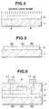
- Figs. 1 to 6 show steps of manufacturing a thin-film transistor according to an embodiment of the present invention. The structure of the thin-film transistor and a method of manufacturing the same will now be described with reference to these drawings in sequence.
- First, as shown in Fig. 1, an amorphous silicon
thin film 2 is deposited on the upper surface of aninsulating substrate 1 made of quartz or the like by an LP-CVD (Low Pressure Chemical Vapor Deposition) method at a temperature of 550°C. Thereafter, as shown in Fig. 2, XeCℓ excimer laser beams are applied to the substrate, thereby polycrystallizing the amorphous siliconthin film 2 into a polysiliconthin film 3 by a liquid-phase growth. The crystal structure of the polysiliconthin film 3 in this state will be described later. Then, as shown in Fig. 3, aphotoresist film 5 is formed on the upper surface of the polysiliconthin film 3, and patterned not to leave on the regions offilm 3 which correspond to source anddrain forming regions 4. Using thephotoresist film 5 as a mask, impurities such as phosphorus ions or boron ions are injected to a high concentration into the source anddrain forming regions 4 of the polysiliconthin film 3, thereby forming impurity-injectedregions 6. Thereafter, thephotoresist film 5 is removed. Next, as shown in Fig. 4, XeCℓ excimer laser beams are applied to the polysiliconthin film 3 again to activate the impurities injected in theregions 6. Then, as shown in Fig. 5, an unneeded peripheral portion of the polysiliconthin film 3 is removed. A central portion of the polysiliconthin film 3 serves as a channel region 3a, and side portions thereof as source anddrain regions 3b formed of activated impurity regions. Subsequently, as shown in Fig. 6, a gate-insulatingfilm 7 formed of a silicon oxide film and the like is formed on the upper surface of the assembly. Thereafter, agate electrode 8 made of chrome and the like is formed on the upper surface of a portion of thegate insulating film 7 which corresponds to the channel region 3a, by means of a depositing and a patterning. Thereafter, a passivating insulating film 9 made of silicon nitride or the like is formed on the entire upper surface of the assembly. Then,contact holes 10 are formed in those portions of the passivating insulating film 9 and the gate-insulatingfilm 7 which correspond to the source anddrain regions 3b. Subsequently, source anddrain electrodes 11 made of aluminum and the like are patterned on the passivating insulating film 9 and connected to the source anddrain regions 3b through thecontact holes 10 are formed on the passivating insulating film 9 and in theholes 10. Thus, a field effect thin-film transistor of a coplanar type is obtained. - The crystal structure of the polysilicon
thin film 3 shown in Fig. 2 will now be described with reference to Table 1.

- As shown in Table 1, a polysilicon thin film according to an embodiment of the present invention was prepared in the following manner: an amorphous silicon thin film having a thickness of about 500 Å was deposited on the upper surface of a quartz substrate, and XeCℓ excimer laser beams were applied twice to the amorphous silicon thin film at a temperature of about 250°C under an energy density of about 300 mJ/cm², so that the amorphous silicon thin film was poly-crystallized in a liquid-phase growth, to obtain a polysilicon thin film. To compare the present embodiment with a conventional device, a polysilicon thin film according to conventional art was prepared in the following manner: an amorphous silicon thin film having a thickness of about 500 Å was deposited on the upper surface of a quartz substrate; the substrate was heated in a nitrogen atmosphere at a temperature of about 600°C for 48 hours, so that the amorphous silicon thin film was polycrystallized in a solid-phase growth, to obtain a polysilicon thin film.
- The crystal structures were analyzed by using a (Transmission Electron Microscope) and an XD (X-ray Diffractor analysis). In case of the TEM, grain size was measured with JEM-2010 of JEOL (acceleration voltage: 200 kV, magnification: 5 × 10⁵ to 1.5 × 10⁶). The grain size of the embodiment was 246 nm, whereas the grain size of the prior art was 1.2 µm, which is 5 times greater than the grain size of the embodiment. The grain size refers to the size of a grain in the top view of the polysilicon thin film, and is represented by an average value of the total of average values c of size of grains obtained by the following equation:


- The crystallite size by use of the XD was measured by detecting a diffraction intensity by using a low angle incidence method, wherein ϑ' = 1°. RU-200 of Rigaku Denki Company (radiation source: CuKa, maximum output: 12 kW) was used for the measurement. In the measurement, step scanning for 2 seconds was performed three times (30 minutes in total) with a rotational angle of 0.01° within a range of ±1.5° on each of the peak planes, i.e., the (111) plane, the (220) plane, and the (311) plane, under the condition of the
incident X-ray intensity 50 kV and the current of 180 mA. The crystallite size was calculated from the peak width at half height by use of the following equation of Scherrer.

where Dhk1 denotes a crystallite size in a direction perpendicular to the (hk1) plane; λ, a wavelength of an X-ray beam; B, a half width; and ϑB, a Bragg's angle. The results of the measurement are shown in Table 1. In the conventional device, the average values of the crystallite size measured in the three-time measurement were 37 nm on the (111) plane, 23 nm on the (220) plane, and 36 nm on the (311) plane, whereas in the present embodiment, the average values were much greater than in the conventional device, i.e., 202 nm on the (111) plane, 144 nm on the (220) plane, and 103 nm on the (311) plane. - Coplanar type field effect thin-film transistors as shown in Fig. 6 were manufactured using the thin films of the embodiment and the conventional art, and the field effect mobilities µFE thereof were measured. As shown in Table 1, the mobility in the conventional thin-film transistor was 30 cm²/V·sec, whereas the mobility in the thin-film transistor of the present embodiment was 90 cm²/V·sec, which is three times greater than that of the conventional transistor. The measurement result represents that the field effect mobility µFE is correlated to the crystallite size rather than the grain size. This appears to be based on the fact that a thin-film transistor wherein the grain size is large and the crystallite size is small includes a number of crystal defects, while a thin-film transistor wherein the crystallite size is substantially the same as the grain size includes few crystal defects, even if the grain size is small, since the crystallite is regarded as a complete monocrystal region.
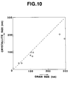
- To confirm this, similar measurement was performed with respect to a number of samples according to the embodiment. Figs. 9A, 9B, and 10 show results of the measurement. Although the sample indicated in Table 1 includes an amorphous silicon film deposited on the substrate to a thickness of 500 Å by a LPCVD method, some of the samples indicated in Figs. 9A, 9B, and 10 are formed by a plasma CVD method or have various thicknesses (500 to 3000 Å). Fig. 9A shows the relationship between grain size


- It is clear from Figs. 9A and 9B that the crystallite size of about 180 nm (measured value) or greater and the grain size


- Further, referring to Table 1, the crystallite sizes on the (111), (220), and (311) planes of the embodiment are respectively 202 nm, 144 nm, and 103 nm, which are all greater than the thickness of the polysilicon thin film, i.e., 500 Å. In contrast, in the conventional device, the crystallite size on the (111) plane, i.e. the maximum peak plane, is 37 nm which is smaller than the thickness of the polysilicon thin film, 500 Å. This proves that the field effect mobility µFE can be more greatly increased than in the conventional device, if the crystallite size of the polysilicon thin film is greater than the thickness of the polysilicon thin film. According to the embodiment, since the thickness of the polysilicon thin film is 500 to 3000 Å, the field effect mobility µFE of at least 50 cm²/V·sec is ensured.
- The present invention is not limited to a field effect thin-film transistor, but is applicable to any type of semiconductor device having a polysilicon thin film as its main part to transfer carriers.
- As has been described above, if a polysilicon thin film has the grain size and the crystallite size substantially the same as each other, the field effect mobility µFE can be greatly increased, accordingly, a driver circuit which is operated with a clock frequency of about 10 MHz can be formed using a semiconductor device. Note that when the crystallite size is 60 to 70 % or greater of the grain size, these sizes are considered to be "substantially the same".
Claims (6)
- A semiconductor device having a polysilicon thin film (3) in its main part, characterized in that a grains size is substantially the same as a crystallite size on the (111) plane and said crystallite size is greater than a thickness of said polysilicon thin film.
- A semiconductor device according to claim 1, characterized in that the average value of the grain size on said (111) plane is at least 200 nm.
- A semiconductor device according to claim 1 or 2, characterized in that the average value of the crystallite size is greater than a thickness of the polysilicon thin film (3).
- A semiconductor device according to claim 1, 2 or 3, characterized in that the polysilicon thin film (3) comprises at least one impurity doped region (3b) in which dopants are diffused and an intrinsic region (3a) which does not include dopants.
- A semiconductor device according to claim 4, characterized in that the impurity doped regions (3b) are arranged on both sides of the intrinsic region (3a).
- A semiconductor device according to claim 5, characterized in that electrodes (8, 11) doped are respectively connected to the impurity region (3b) and the intrinsic region (3a) directly or indirectly.
Applications Claiming Priority (3)
| Application Number | Priority Date | Filing Date | Title |
|---|---|---|---|
| JP75921/92 | 1992-02-28 | ||
| JP4075921A JP2935446B2 (en) | 1992-02-28 | 1992-02-28 | Semiconductor device |
| JP7592192 | 1992-02-28 |
Publications (3)
| Publication Number | Publication Date |
|---|---|
| EP0558075A2 true EP0558075A2 (en) | 1993-09-01 |
| EP0558075A3 EP0558075A3 (en) | 1994-01-19 |
| EP0558075B1 EP0558075B1 (en) | 2004-08-18 |
Family
ID=13590260
Family Applications (1)
| Application Number | Title | Priority Date | Filing Date |
|---|---|---|---|
| EP93103140A Expired - Lifetime EP0558075B1 (en) | 1992-02-28 | 1993-02-26 | Method for fabricating a polysilicon thin film transistor |
Country Status (10)
| Country | Link |
|---|---|
| US (1) | US5949091A (en) |
| EP (1) | EP0558075B1 (en) |
| JP (1) | JP2935446B2 (en) |
| KR (1) | KR970004844B1 (en) |
| CN (1) | CN1026041C (en) |
| CA (1) | CA2090096C (en) |
| DE (1) | DE69333592T2 (en) |
| HK (1) | HK1013521A1 (en) |
| SG (1) | SG55060A1 (en) |
| TW (1) | TW335216U (en) |
Cited By (1)
| Publication number | Priority date | Publication date | Assignee | Title |
|---|---|---|---|---|
| US6670638B2 (en) * | 2000-09-25 | 2003-12-30 | Hitachi, Ltd. | Liquid crystal display element and method of manufacturing the same |
Families Citing this family (8)
| Publication number | Priority date | Publication date | Assignee | Title |
|---|---|---|---|---|
| TW264575B (en) * | 1993-10-29 | 1995-12-01 | Handotai Energy Kenkyusho Kk | |
| US6059873A (en) | 1994-05-30 | 2000-05-09 | Semiconductor Energy Laboratory Co., Ltd. | Optical processing method with control of the illumination energy of laser light |
| US6100119A (en) * | 1995-08-31 | 2000-08-08 | Lg Electronics Inc. | Thin film transistor and method for fabricating the same |
| JPH11145056A (en) * | 1997-11-07 | 1999-05-28 | Sony Corp | Semiconductor material |
| JP2000208771A (en) * | 1999-01-11 | 2000-07-28 | Hitachi Ltd | Semiconductor device, liquid cystal display device, and their manufacturing |
| JP4437570B2 (en) * | 1999-07-12 | 2010-03-24 | 株式会社ルネサステクノロジ | Semiconductor device and manufacturing method of semiconductor device |
| US6229611B1 (en) * | 1999-09-20 | 2001-05-08 | United Microelectronics Corp. | Method of detecting a transparent quartz wafer in a semiconductor equipment |
| JP6941473B2 (en) * | 2017-04-26 | 2021-09-29 | 株式会社日本製鋼所 | Display manufacturing method, display and LCD TV |
Citations (4)
| Publication number | Priority date | Publication date | Assignee | Title |
|---|---|---|---|---|
| JPS57194517A (en) * | 1981-05-27 | 1982-11-30 | Toshiba Corp | Manufacture of semiconductor crystal film |
| FR2573916A1 (en) * | 1984-11-26 | 1986-05-30 | Sony Corp | METHOD FOR MANUFACTURING THIN SEMICONDUCTOR FILM AND FILM THUS OBTAINED |
| JPS63292618A (en) * | 1987-05-26 | 1988-11-29 | Nec Corp | Manufacture of soi substrate |
| JPH02148831A (en) * | 1988-11-30 | 1990-06-07 | Hitachi Ltd | Laser annealing method |
Family Cites Families (8)
| Publication number | Priority date | Publication date | Assignee | Title |
|---|---|---|---|---|
| JPH0620122B2 (en) * | 1982-01-19 | 1994-03-16 | キヤノン株式会社 | Semiconductor element |
| US4649624A (en) * | 1983-10-03 | 1987-03-17 | The United States Of America As Represented By The Secretary Of The Navy | Fabrication of semiconductor devices in recrystallized semiconductor films on electrooptic substrates |
| US5200630A (en) * | 1989-04-13 | 1993-04-06 | Sanyo Electric Co., Ltd. | Semiconductor device |
| JP2655924B2 (en) * | 1990-02-19 | 1997-09-24 | キヤノン株式会社 | Polycrystalline semiconductor thin film forming method |
| JP2973492B2 (en) * | 1990-08-22 | 1999-11-08 | ソニー株式会社 | Crystallization method of semiconductor thin film |
| EP0499979A3 (en) * | 1991-02-16 | 1993-06-09 | Semiconductor Energy Laboratory Co., Ltd. | Electro-optical device |
| JPH04267517A (en) * | 1991-02-22 | 1992-09-24 | Toshiba Corp | Formation method of semiconductor thin film |
| JPH04311038A (en) * | 1991-04-09 | 1992-11-02 | Toshiba Corp | Manufacturing method of thin film transistor |
-
1992
- 1992-02-28 JP JP4075921A patent/JP2935446B2/en not_active Expired - Lifetime
-
1993
- 1993-02-20 KR KR1019930002385A patent/KR970004844B1/en not_active IP Right Cessation
- 1993-02-22 CA CA002090096A patent/CA2090096C/en not_active Expired - Lifetime
- 1993-02-23 US US08/021,333 patent/US5949091A/en not_active Expired - Lifetime
- 1993-02-25 TW TW084217964U patent/TW335216U/en unknown
- 1993-02-26 CN CN93101559A patent/CN1026041C/en not_active Expired - Lifetime
- 1993-02-26 EP EP93103140A patent/EP0558075B1/en not_active Expired - Lifetime
- 1993-02-26 DE DE69333592T patent/DE69333592T2/en not_active Expired - Lifetime
- 1993-02-26 SG SG1996004011A patent/SG55060A1/en unknown
-
1998
- 1998-12-22 HK HK98114686A patent/HK1013521A1/en not_active IP Right Cessation
Patent Citations (4)
| Publication number | Priority date | Publication date | Assignee | Title |
|---|---|---|---|---|
| JPS57194517A (en) * | 1981-05-27 | 1982-11-30 | Toshiba Corp | Manufacture of semiconductor crystal film |
| FR2573916A1 (en) * | 1984-11-26 | 1986-05-30 | Sony Corp | METHOD FOR MANUFACTURING THIN SEMICONDUCTOR FILM AND FILM THUS OBTAINED |
| JPS63292618A (en) * | 1987-05-26 | 1988-11-29 | Nec Corp | Manufacture of soi substrate |
| JPH02148831A (en) * | 1988-11-30 | 1990-06-07 | Hitachi Ltd | Laser annealing method |
Non-Patent Citations (8)
| Title |
|---|
| APPLIED PHYSICS LETTERS vol. 59, no. 27 , 30 December 1991 , NEW YORK US pages 3565 - 3567 HIDEYA KUMOMI ET AL 'Manipulation of nucleation sites in solid.state Si crystallization' * |
| IEEE TRANSACTIONS ON ELECTRON DEVICES vol. 35, no. 7 , July 1988 , NEW YORK US pages 923 - 928 TERUO KATOH 'Characteristics of MOSFET s on Large-Grain Polysilicon Films' * |
| JAPANESE JOURNAL OF APPLIED PHYSICS, SUPPLEMENTS 1983 , TOKYO JA pages 35 - 38 YUTAKA KOBAYASHI ET AL 'Recrystallization of Polycrystalline Silicon Islands on Fused Silica' * |
| MATERIALS RESEARCH SOCIETY December 1986 , PITTSBURG, PA, USA pages 319 - 325 J. A. ROTH ET AL 'EFFECTS OF IMPURITIES ON THE KINETICS OF NUCLEATION AND GROWTH IN AMORPHOUS SILICON' * |
| PATENT ABSTRACTS OF JAPAN vol. 007, no. 045 (E-160)23 February 1983 & JP-A-57 194 517 (TOKYO SHIBAURA DENKI KK) 30 November 1982 * |
| PATENT ABSTRACTS OF JAPAN vol. 013, no. 123 (E-733)27 March 1989 & JP-A-63 292 618 (NEC CORP) 29 November 1988 * |
| PATENT ABSTRACTS OF JAPAN vol. 014, no. 396 (E-0970)27 August 1990 & JP-A-02 148 831 (HITACHI LTD) 7 June 1990 * |
| SASAKI M. ET AL: 'Lateral solid phase epitaxy of Si over SiO2 patterns and its application to silicon-on-insulator transistors' APPLIED PHYSICS LETTERS vol. 49, no. 7, 18 August 1986, pages 397 - 399 * |
Cited By (1)
| Publication number | Priority date | Publication date | Assignee | Title |
|---|---|---|---|---|
| US6670638B2 (en) * | 2000-09-25 | 2003-12-30 | Hitachi, Ltd. | Liquid crystal display element and method of manufacturing the same |
Also Published As
| Publication number | Publication date |
|---|---|
| DE69333592D1 (en) | 2004-09-23 |
| EP0558075B1 (en) | 2004-08-18 |
| KR970004844B1 (en) | 1997-04-04 |
| US5949091A (en) | 1999-09-07 |
| DE69333592T2 (en) | 2005-01-05 |
| CN1076551A (en) | 1993-09-22 |
| SG55060A1 (en) | 1998-12-21 |
| JP2935446B2 (en) | 1999-08-16 |
| JPH05243576A (en) | 1993-09-21 |
| KR930018754A (en) | 1993-09-22 |
| CN1026041C (en) | 1994-09-28 |
| CA2090096A1 (en) | 1993-08-29 |
| HK1013521A1 (en) | 1999-08-27 |
| TW335216U (en) | 1998-06-21 |
| EP0558075A3 (en) | 1994-01-19 |
| CA2090096C (en) | 1998-08-11 |
Similar Documents
| Publication | Publication Date | Title |
|---|---|---|
| EP0459763B1 (en) | Thin-film transistors | |
| US7238558B2 (en) | Semiconductor device and method of fabricating the same | |
| US5637515A (en) | Method of making thin film transistor using lateral crystallization | |
| US5864150A (en) | Hybrid polysilicon/amorphous silicon TFT and method of fabrication | |
| US6271062B1 (en) | Thin film semiconductor device including a semiconductor film with high field-effect mobility | |
| US5696386A (en) | Semiconductor device | |
| EP0523768B1 (en) | Thin-film transistor manufacture | |
| US5231297A (en) | Thin film transistor | |
| US20010000154A1 (en) | Thin film type monolithic semiconductor device | |
| US5576229A (en) | Method of fabricating a thin-film transistor and liquid-crystal display apparatus | |
| US5877526A (en) | Semiconductor device having polysilicon thin-film | |
| EP0459836B1 (en) | Method for fabricating thin-film transistors | |
| EP0558075A2 (en) | Polysilicon thin film semiconductor device | |
| US5733793A (en) | Process formation of a thin film transistor | |
| US5937304A (en) | Method for fabricating semiconductor device and method for producing liquid crystal display apparatus | |
| US6639245B2 (en) | Active matrix display device having high intensity and high precision and manufacturing method thereof | |
| JPH0897436A (en) | Thin film semiconductor device and its manufacture | |
| JPH04340725A (en) | Manufacture of thin film transistor | |
| JPH04340724A (en) | Manufacture of thin film transistor | |
| JPH0888172A (en) | Manufacture of polycrystalline silicon film | |
| KR0138874B1 (en) | Tft fabrication method | |
| JPH08186262A (en) | Manufacture of thin film transistor | |
| JPH07193252A (en) | Thin film transistor and its manufacture | |
| JP3430743B2 (en) | Method for manufacturing thin film transistor | |
| JP3244387B2 (en) | Thin film semiconductor device |
Legal Events
| Date | Code | Title | Description |
|---|---|---|---|
| PUAI | Public reference made under article 153(3) epc to a published international application that has entered the european phase |
Free format text: ORIGINAL CODE: 0009012 |
|
| 17P | Request for examination filed |
Effective date: 19930226 |
|
| AK | Designated contracting states |
Kind code of ref document: A2 Designated state(s): DE FR GB |
|
| PUAL | Search report despatched |
Free format text: ORIGINAL CODE: 0009013 |
|
| AK | Designated contracting states |
Kind code of ref document: A3 Designated state(s): DE FR GB |
|
| 17Q | First examination report despatched |
Effective date: 19960320 |
|
| APAB | Appeal dossier modified |
Free format text: ORIGINAL CODE: EPIDOS NOAPE |
|
| APAB | Appeal dossier modified |
Free format text: ORIGINAL CODE: EPIDOS NOAPE |
|
| APAD | Appeal reference recorded |
Free format text: ORIGINAL CODE: EPIDOS REFNE |
|
| APAB | Appeal dossier modified |
Free format text: ORIGINAL CODE: EPIDOS NOAPE |
|
| RAP1 | Party data changed (applicant data changed or rights of an application transferred) |
Owner name: CASIO COMPUTER CO., LTD. |
|
| RTI1 | Title (correction) |
Free format text: METHOD FOR FABRICATING A POLYSILICON THIN FILM TRANSISTOR |
|
| GRAG | Despatch of communication of intention to grant |
Free format text: ORIGINAL CODE: EPIDOS AGRA |
|
| RIC1 | Information provided on ipc code assigned before grant |
Free format text: 6H 01L 29/04 A, 6H 01L 29/16 B, 6H 01L 21/20 B, 6H 01L 29/786 B |
|
| RTI1 | Title (correction) |
Free format text: METHOD FOR FABRICATING A POLYSILICON THIN FILM TRANSISTOR |
|
| GRAG | Despatch of communication of intention to grant |
Free format text: ORIGINAL CODE: EPIDOS AGRA |
|
| APAB | Appeal dossier modified |
Free format text: ORIGINAL CODE: EPIDOS NOAPE |
|
| APAB | Appeal dossier modified |
Free format text: ORIGINAL CODE: EPIDOS NOAPE |
|
| APAD | Appeal reference recorded |
Free format text: ORIGINAL CODE: EPIDOS REFNE |
|
| APAB | Appeal dossier modified |
Free format text: ORIGINAL CODE: EPIDOS NOAPE |
|
| APBT | Appeal procedure closed |
Free format text: ORIGINAL CODE: EPIDOSNNOA9E |
|
| GRAP | Despatch of communication of intention to grant a patent |
Free format text: ORIGINAL CODE: EPIDOSNIGR1 |
|
| RIC1 | Information provided on ipc code assigned before grant |
Ipc: 7H 01L 29/786 B Ipc: 7H 01L 21/20 B Ipc: 7H 01L 29/16 B Ipc: 7H 01L 29/04 A |
|
| RTI1 | Title (correction) |
Free format text: METHOD FOR FABRICATING A POLYSILICON THIN FILM TRANSISTOR |
|
| RIC1 | Information provided on ipc code assigned before grant |
Ipc: 7H 01L 29/786 B Ipc: 7H 01L 21/20 B Ipc: 7H 01L 29/16 B Ipc: 7H 01L 29/04 A |
|
| RTI1 | Title (correction) |
Free format text: METHOD FOR FABRICATING A POLYSILICON THIN FILM TRANSISTOR |
|
| RIC1 | Information provided on ipc code assigned before grant |
Ipc: 7H 01L 29/786 B Ipc: 7H 01L 21/20 B Ipc: 7H 01L 29/16 B Ipc: 7H 01L 29/04 A |
|
| RTI1 | Title (correction) |
Free format text: METHOD FOR FABRICATING A POLYSILICON THIN FILM TRANSISTOR |
|
| RIC1 | Information provided on ipc code assigned before grant |
Ipc: 7H 01L 29/786 B Ipc: 7H 01L 21/20 B Ipc: 7H 01L 29/16 B Ipc: 7H 01L 29/04 A |
|
| RTI1 | Title (correction) |
Free format text: METHOD FOR FABRICATING A POLYSILICON THIN FILM TRANSISTOR |
|
| GRAS | Grant fee paid |
Free format text: ORIGINAL CODE: EPIDOSNIGR3 |
|
| GRAA | (expected) grant |
Free format text: ORIGINAL CODE: 0009210 |
|
| GRAU | Approval following communication of intention to grant |
Free format text: ORIGINAL CODE: EPIDOSNAGR4 |
|
| AK | Designated contracting states |
Kind code of ref document: B1 Designated state(s): DE FR GB |
|
| REG | Reference to a national code |
Ref country code: GB Ref legal event code: FG4D |
|
| REF | Corresponds to: |
Ref document number: 69333592 Country of ref document: DE Date of ref document: 20040923 Kind code of ref document: P |
|
| GRAN | Information related to approval following communication of intention to grant deleted |
Free format text: ORIGINAL CODE: EPIDOSDAGR4 |
|
| GRAS | Grant fee paid |
Free format text: ORIGINAL CODE: EPIDOSNIGR3 |
|
| REG | Reference to a national code |
Ref country code: HK Ref legal event code: GR Ref document number: 1013521 Country of ref document: HK |
|
| ET | Fr: translation filed | ||
| PLBE | No opposition filed within time limit |
Free format text: ORIGINAL CODE: 0009261 |
|
| STAA | Information on the status of an ep patent application or granted ep patent |
Free format text: STATUS: NO OPPOSITION FILED WITHIN TIME LIMIT |
|
| 26N | No opposition filed |
Effective date: 20050519 |
|
| APAH | Appeal reference modified |
Free format text: ORIGINAL CODE: EPIDOSCREFNO |
|
| PGFP | Annual fee paid to national office [announced via postgrant information from national office to epo] |
Ref country code: FR Payment date: 20120221 Year of fee payment: 20 |
|
| PGFP | Annual fee paid to national office [announced via postgrant information from national office to epo] |
Ref country code: DE Payment date: 20120222 Year of fee payment: 20 |
|
| PGFP | Annual fee paid to national office [announced via postgrant information from national office to epo] |
Ref country code: GB Payment date: 20120222 Year of fee payment: 20 |
|
| REG | Reference to a national code |
Ref country code: DE Ref legal event code: R071 Ref document number: 69333592 Country of ref document: DE |
|
| REG | Reference to a national code |
Ref country code: FR Ref legal event code: TP Owner name: REMSEN INNOVATION, LLC., US Effective date: 20130207 |
|
| REG | Reference to a national code |
Ref country code: GB Ref legal event code: PE20 Expiry date: 20130225 |
|
| REG | Reference to a national code |
Ref country code: GB Ref legal event code: 732E Free format text: REGISTERED BETWEEN 20130314 AND 20130320 |
|
| REG | Reference to a national code |
Ref country code: DE Ref legal event code: R082 Ref document number: 69333592 Country of ref document: DE Representative=s name: GRUENECKER, KINKELDEY, STOCKMAIR & SCHWANHAEUS, DE Effective date: 20130227 Ref country code: DE Ref legal event code: R081 Ref document number: 69333592 Country of ref document: DE Owner name: REMSEN INNOVATION, LLC, US Free format text: FORMER OWNER: CASIO COMPUTER CO., LTD., TOKIO/TOKYO, JP Effective date: 20130227 |
|
| PG25 | Lapsed in a contracting state [announced via postgrant information from national office to epo] |
Ref country code: DE Free format text: LAPSE BECAUSE OF EXPIRATION OF PROTECTION Effective date: 20130227 Ref country code: GB Free format text: LAPSE BECAUSE OF EXPIRATION OF PROTECTION Effective date: 20130225 |