EP0555779B1 - TTL/CMOS-Eingangspuffer mit Unterdrückung von Störimpulsen und mit geringem Energieverbrauch - Google Patents
TTL/CMOS-Eingangspuffer mit Unterdrückung von Störimpulsen und mit geringem Energieverbrauch Download PDFInfo
- Publication number
- EP0555779B1 EP0555779B1 EP93101807A EP93101807A EP0555779B1 EP 0555779 B1 EP0555779 B1 EP 0555779B1 EP 93101807 A EP93101807 A EP 93101807A EP 93101807 A EP93101807 A EP 93101807A EP 0555779 B1 EP0555779 B1 EP 0555779B1
- Authority
- EP
- European Patent Office
- Prior art keywords
- channel transistor
- input
- gate
- translator
- drain
- Prior art date
- Legal status (The legal status is an assumption and is not a legal conclusion. Google has not performed a legal analysis and makes no representation as to the accuracy of the status listed.)
- Expired - Lifetime
Links
Images



Classifications
-
- H—ELECTRICITY
- H03—ELECTRONIC CIRCUITRY
- H03K—PULSE TECHNIQUE
- H03K3/00—Circuits for generating electric pulses; Monostable, bistable or multistable circuits
- H03K3/02—Generators characterised by the type of circuit or by the means used for producing pulses
- H03K3/353—Generators characterised by the type of circuit or by the means used for producing pulses by the use, as active elements, of field-effect transistors with internal or external positive feedback
- H03K3/356—Bistable circuits
- H03K3/356017—Bistable circuits using additional transistors in the input circuit
-
- H—ELECTRICITY
- H03—ELECTRONIC CIRCUITRY
- H03K—PULSE TECHNIQUE
- H03K3/00—Circuits for generating electric pulses; Monostable, bistable or multistable circuits
- H03K3/01—Details
- H03K3/012—Modifications of generator to improve response time or to decrease power consumption
-
- H—ELECTRICITY
- H03—ELECTRONIC CIRCUITRY
- H03K—PULSE TECHNIQUE
- H03K3/00—Circuits for generating electric pulses; Monostable, bistable or multistable circuits
- H03K3/01—Details
- H03K3/013—Modifications of generator to prevent operation by noise or interference
-
- H—ELECTRICITY
- H03—ELECTRONIC CIRCUITRY
- H03K—PULSE TECHNIQUE
- H03K3/00—Circuits for generating electric pulses; Monostable, bistable or multistable circuits
- H03K3/02—Generators characterised by the type of circuit or by the means used for producing pulses
- H03K3/353—Generators characterised by the type of circuit or by the means used for producing pulses by the use, as active elements, of field-effect transistors with internal or external positive feedback
- H03K3/356—Bistable circuits
- H03K3/356104—Bistable circuits using complementary field-effect transistors
- H03K3/356113—Bistable circuits using complementary field-effect transistors using additional transistors in the input circuit
Definitions
- TTL-to-CMOS level translating buffer circuits incorporating multiple stages with feedback and forward couplings between stages that eliminate the static current when TTL high potential level data signals are applied at the buffer circuit input.
- the feedback and feed forward couplings maintain and enhance signal propagation speed in the buffer circuits at the same time.
- TTL-to-CMOS translating latch circuits and flip-flop circuits similarly incorporate feedback and feedforward circuit couplings to save and retain data signals during latch mode, static mode, and tristate mode operation while at the same time substantially eliminating static high current.
- N-channel transistor 14 results in Vout being less than 0.8 volts, which is a logic zero.
- the problem with a logic one input of two volts is that neither P-channel transistor 16 nor N-channel transistor 14 are completely turned off, which allows a significant DC current to be drawn from Vcc. This current is a function of the actual transistor sizes, it can typically range from as little as 0.1 mA to over one milliamp.
- a further advantage of the present invention is that input noise rejection is improved.
- a further advantage of the present invention is that current consuming reference voltage circuits found in prior art TTL-to-CMOS input buffers are eliminated.
- a further advantage of the present invention is that an area savings is realized on a chip with many TTL compatible inputs.
- P-channel transistor 27 when Vin is greater than 2.0 volts, P-channel transistor 27 will have a gate-to-source voltage (Vgs) greater than -0.8 volts, which is greater than -1.1 volts, turning off P-channel transistor 27.
- Vgs gate-to-source voltage
- N-channel transistor 21 When Vin is less than 0.8 volts, N-channel transistor 21 will turn off.
- the output of this inverter, node 44 will swing from about 2.8 volts to ground when Vin swings from less than 0.8 volts to greater than 2.0 volts.
- node 44 still switches in less than one nanosecond, because it only has to drive the small capacitance of the gate of N-channel transistor 22.
- the TTL-level input signal may be passed through an input protection network prior to being received by the input buffer of the present invention.
- a pair of cross-coupled inverters 46 and 48 can be viewed as an RS Flip-Flop with the "set” and “reset” inputs labelled as Vin and node 44 respectively.
- the TRUE output is a node 50.
- N-channel transistors 22 and 23 are sized to have much more gain than P-channel transistors 30 and 31. In fact, P-channel transistors 30 and 31 are intentionally sized very long and narrow, so that the signal rise times of nodes 50 and 52 will be relatively slow.
- Transistors 24 and 25 and transistors 33 and 34 make up a two-input NOR gate 54 having its inputs supplied by nodes Vin and 50, as shown in Fig. 2.
- the transistor sizes in NOR gate 54 are adjusted so that its output node 56 switches when Vin is at about 2.5 volts and node 50 is at ground (zero volts).
- P-channel transistor 32 pulls node 50 quickly and completely to Vcc, once node 56 starts to go low, thus making for a shorter fall time for node 56.
- P-channel transistor 35 and N-channel transistor 26 are simply a buffering inverter for driving capacitive loads.
- FIG. 3 A second embodiment of the present invention is shown in Fig. 3.
- the voltage dropping function of transistors 28 and 29 (Fig. 2) can be accomplished by other means.
- the forward voltage drop of a set of three diodes 60, 62, and 64, in series, is used for the voltage dropping function.
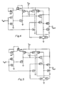
- Fig. 4 shows a third embodiment of the present invention wherein the voltage dropping function of transistors 28 and 29 is accomplished by a pair of N-channel transistors 70 and 72 which have their gates connected to their respective drains.
- Fig. 5 shows a fourth embodiment of the present invention wherein the voltage dropping function of transistors 28 and 29 is accomplished by a P-channel transistor 80 in series with an N-channel transistor 82, effectively replacing P-channel transistor 28 with N-channel transistor 82.
- the voltage dropping function may be achieved by an N-channel transistor with its gate and drain tied to a positive voltage supply and its source connected to the drain of a P-channel transistor.
- This P-channel transistor would have its gate and drain tied together.
- Fig. 6 it can be seen that initializing Vin at 0.8 volts will result in the voltage at node 44 being approximately 2.8 volts, the voltage at node 50 being zero, the voltage at nodes 52 and 56 being approximately equal to Vcc, and the voltage at node 58 being zero.
- a rapid rise of Vin to 2.0 volts causes a rapid fall of the voltage at node 44 to zero volts and a rapid fall of the voltage at node 52 to zero volts.
- Node 52 being at zero volts will turn on P-channel transistor 30, causing node 44 to rise slowly.
- N-channel transistor 24 and N-channel transistor 25 are turned off, and P-channel transistor 33 and P-channel transistor 34 are turned on, which makes node 56 rise rapidly, and node 58 fall rapidly.
- P-channel transistor 32 is turned off after node 56 rises to Vcc.
- Vin falls from 0.8 volts to zero volts in preparation for simulation of the rise of the buffer input signal from zero volts to 3.0 volts for the AC portion of the simulation.
- This rise to 3.0 volts of Vin causes nodes 44 and 52 to almost immediately drop to zero volts.
- Node 50 will start to slowly rise.
- three volts is a high enough level on one input of NOR gate 54 for output node 56 to almost immediately begin falling, without waiting for node 50 to rise.
- P-channel transistor 32 is again turned on and almost immediately pulls node 50 to Vcc.
- Vin required to switch node 56 low is determined by the sizes of N-channel transistor 24, N-channel transistor 25, P-channel transistor 33, and P-channel transistor 34.
- a typical switching point being Vin at approximately 2.5 volts.
- Vin fall from 3.0 volts to zero volts, node 56 does not switch high for the same Vin that caused it to switch low, because now node 50 is at Vcc.
- Node 56 will not switch low again until Vin falls low enough to cause node 44 to rise and node 50 to fall.
- Node 44 will start rising when Vin falls to less than 1.4 volts, just as in the above-described DC portion of the simulation.
- a leakage-current-only result is achieved for the case of Vin > 2.0 volts because P-channel transistor 22 is off when its source is 2.8 volts and its gate is greater than 2.0 volts.
- N-channel transistor 21 is on, which makes node 44 low, which turns off N-channel transistor 22.
- N-channel transistor 23 is on, pulling node 52 low, which turns on P-channel transistor 30, which pulls node 50 to Vcc, because N-channel transistor 22 is off.
- Vin high and node 50 at Vcc N-channel transistor 24 and N-channel transistor 25 are on.
- P-channel transistor 33 is off, and P-channel transistor 34 is partially on, because its gate is greater than 2.0 volts but not at Vcc.
- node 56 will be at ground which turns on P-channel transistor 32, and which further causes node 58 to be at Vcc, with P-channel transistor 35 on and N-channel transistor 26 off. There will be no conducting paths from Vcc to ground, because:
Landscapes
- Logic Circuits (AREA)
Claims (15)
- Rauschunterdrückender, leistungsarmer TTL-zu-CMOS-Logikpegelumsetzer mit folgenden Merkmalen:zwei Spannungsversorgungsanschlüssen, wobei einer der Anschlüsse (VCC) ein positiver Spannungsanschluß und der andere ein elektrischer Masseanschluß ist,eine Eingangseinrichtung (VIN),eine Einrichtung (P2, P3; D1-D3; N7, N8; P3, N7) zum Verringern einer positiven Versorgungsspannung, die einen Eingang, der mit dem positiven Spannungsanschluß (VCC) verbunden ist, und einen Ausgang aufweist,eine erste Inverterschaltung (P1, N1) mit einem ersten Spannungsversorgungsanschluß, der mit dem Ausgang der Reduziereinrichtung verbunden ist, mit einem zweiten Spannungsversorgungsanschluß, der mit der elektrischen Masse verbunden ist, mit einem Eingang, der mit der Eingangseinrichtung (VIN) verbunden ist, und mit einem Ausgang,ein CMOS-Setz-Rücksetz-Flip-Flop (46, 48; N2, P4, N3, P5) mit einem Setzeingang, der mit der Eingangseinrichtung (VIN) verbunden ist, mit einem Rücksetzeingang, der mit dem ersten Inverter (P1, N1) verbunden ist, und mit einem Wahr-Ausgang (50),gekennzeichnet durch
ein NOR-Gatter (N4, N5, P7, P8) mit zwei Eingängen, wobei ein Eingang mit der Eingangseinrichtung (VIN) und der andere Eingang mit dem Wahr-Ausgang des Flip-Flops verbunden ist, und mit einem Ausgang (58) zum Übertragen der Pegel-umgesetzten TTL-Eingangssignale. - Umsetzer nach Anspruch 1, ferner gekennzeichnet durch einen zweiten Inverter (26, 35; N6, P9) der elektrisch mit dem positiven Spannungsanschluß (VCC) und der elektrischen Masse verbunden ist, und einen Eingang und einen Ausgang aufweist, wobei der Eingang des zweiten Inverters mit dem Ausgang des zwei Eingänge aufweisenden NOR-Gatters verbunden ist.
- Umsetzer nach Anspruch 2, dadurch gekennzeichnet, daß der zweite Inverter einen P-Kanal-Transistor (35, 9) und einen N-Kanal-Transistor (26, N6) aufweist, die elektrisch in Reihe geschaltet sind, wobei der P-Kanalund der N-Kanal-Transistor die gleiche gezeichnete Breite und Länge aufweisen.
- Umsetzer nach Anspruch 1, dadurch gekennzeichnet, daß die Eingangs-Einrichtung (VIN) eine Eingangsschutzschaltung aufweist.
- Umsetzer nach Anspruch 1, dadurch gekennzeichnet, daß die Einrichtung zum Verringern einer positiven Versorgungsspannung mehrere P-Kanal-Transistoren (28, 29) aufweist.
- Umsetzer nach Anspruch 1, dadurch gekennzeichnet, daß die Einrichtung zum Verringern einer positiven Versorgungsspannung einen ersten P-Kanal-Transistor (29) aufweist, dessen Source elektrisch mit dem positiven Spannungsanschluß verbunden ist, und dessen Gate und Drain elektische miteinander verbunden sind, und einen zweiten P-Kanal-Transistor (28) aufweist, dessen Source elektrisch mit dem Drain des ersten P-Kanal-Transistors und dessen Gate und Drain elektrisch miteinander verbunden sind.
- Umsetzer nach Anspruch 1, dadurch gekennzeichnet, daß die Einrichtung zum Verringern einer positiven Versorgungsspannung eine erste Diode (60), deren Anode eletrisch mit dem positiven Spannungsanschluß (VCC) verbunden ist, eine zweite Diode (62), deren Anode elektrisch mit der Kathode der ersten Diode (60) verbunden ist, sowie eine dritte Diode (64) aufweist, deren Anode elektrisch mit der Kathode der zweiten Diode (62) verbunden ist.
- Umsetzer nach Anspruch 1, dadurch gekennzeichnet, daß die Einrichtung zum Verringern einer positiven Versorgungsspannung einen ersten N-Kanal-Transistor (70), dessen Gate und Drain elektrisch mit dem positiven Spannungsanschluß (VCC) verbunden sind, und einen zweiten N-Kanal-Transistor (72) aufweist, dessen Gate und Drain elektrisch mit der Source des ersten N-Kanal-Transistors (70) verbunden sind.
- Umsetzer nach Anspruch 1, dadurch gekennzeichnet, daß die Einrichtung zum Verringern einer positiven Versorgungsspannung einen P-Kanal-Transistor (80), dessen Source elektrisch mit dem positiven Spannungsanschluß (VCC) verbunden ist, und dessen Gate und Drain miteinander verbunden sind, sowie einen N-Kanal-Transistor (82) aufweist, dessen Gate und Drain elektrisch mit dem Gate und Drain des P-Kanal-Transistors (80) verbunden ist.
- Umsetzer nach Anspruch 1, dadurch gekennzeichnet, daß die Einrichtung zum Verringern einer positiven Versorgungsspannung einen N-Kanal-Transistor, dessen Gate und Drain mit dem positiven Spannungsanschluß verbunden sind, sowie einen P-Kanal-Transisitor aufweist, dessen Source elektrisch mit der Source des N-Kanal-Transistors verbunden ist und dessen Gate und Drain miteinander verbunden sind.
- Umsetzer nach Anspruch 1, dadurch gekennzeichnet, daß das CMOS-Setz-Rücksetz-Flip-Flop folgende Merkmale aufweist:einen ersten P-Kanal-Transistor (30), dessen Source mit dem positiven Spannungsversorgungsanschluß (VCC) verbunden ist,einen ersten N-Kanal-Transistor (22), dessen Drain mit dem Drain des ersten P-Kanal-Transistors (30), dessen Source mit der elektrischen Masse und dessen Gate mit dem Rücksetzeingang verbunden sind,einen zweiten P-Kanal-Transistor (31), dessen Source mit dem positiven Spannungsversorgungsanschluß (VCC) und dessen Gate mit dem Drain des ersten P-Kanal-Transistors (30) verbunden ist, undeinen zweiten N-Kanal-Transistor (23), dessen Drain mit dem Drain des zweiten P-Kanal-Transistors (31), dessen Source mit der elektrischen Masse und dessen Gate mit dem Setzeingang verbunden sind.
- Umsetzer nach Anspruch 5, dadurch gekennzeichnet, daß die P-Kanal-Transistoren (28, 29) jeweils in einer einzelnen N-Mulde ausgebildet sind, und daß die jeweilige Source jedes P-Kanal-Transistors mit ihrer jeweiligen N-Mulde verbunden ist.
- Umsetzer nach Anspruch 1, dadurch gekennzeichnet, daß der erste Inverter einen P-Kanal-Transistor (27) und einen N-Kanal-Transistor (21) aufweist, die in Reihe geschaltet sind, wobei daß B/L-Verhältnis des P-Kanal-Transistors etwa doppelt so groß ist wie das B/L-Verhältnis des N-Kanal-Transistors.
- Umsetzer nach einem der Ansprüche 1 bis 13, gekennzeichnet durch einen P-Kanal-Beschleunigungs-Pullup-Transistors, der zwischen die positive Spannungsversorgung (VCC) und den Wahr-Ausgang (50) des ersten Flip-Flop geschaltet ist.
- Umsetzer nach einem der Ansprüche 1 bis 14, dadurch gekennzeichnet, daß das CMOS-Setz-Rücksetz-Flip-Flop (46, 48) relativ kurze Abfallzeiten und relativ lange Anstiegszeiten für seine Ausgangssignale hat.
Applications Claiming Priority (2)
| Application Number | Priority Date | Filing Date | Title |
|---|---|---|---|
| US835207 | 1992-02-13 | ||
| US07/835,207 US5216299A (en) | 1992-02-13 | 1992-02-13 | Low power noise rejecting TTL to CMOS input buffer |
Publications (2)
| Publication Number | Publication Date |
|---|---|
| EP0555779A1 EP0555779A1 (de) | 1993-08-18 |
| EP0555779B1 true EP0555779B1 (de) | 1997-10-22 |
Family
ID=25268919
Family Applications (1)
| Application Number | Title | Priority Date | Filing Date |
|---|---|---|---|
| EP93101807A Expired - Lifetime EP0555779B1 (de) | 1992-02-13 | 1993-02-05 | TTL/CMOS-Eingangspuffer mit Unterdrückung von Störimpulsen und mit geringem Energieverbrauch |
Country Status (5)
| Country | Link |
|---|---|
| US (1) | US5216299A (de) |
| EP (1) | EP0555779B1 (de) |
| JP (1) | JPH066205A (de) |
| CA (1) | CA2089429C (de) |
| DE (1) | DE69314676D1 (de) |
Families Citing this family (13)
| Publication number | Priority date | Publication date | Assignee | Title |
|---|---|---|---|---|
| US5296758A (en) * | 1992-02-24 | 1994-03-22 | National Semiconductor Corporation | Output buffer with ground bounce compensation |
| US5602496A (en) * | 1992-06-17 | 1997-02-11 | Advanced Micro Devices, Inc. | Input buffer circuit including an input level translator with sleep function |
| KR100392556B1 (ko) * | 1994-01-31 | 2003-11-12 | 주식회사 하이닉스반도체 | 시모스회로용입력버퍼 |
| FR2719727B1 (fr) * | 1994-05-03 | 1996-07-26 | Matra Mhs | Circuit de sortie pour circuit intégré. |
| US6194945B1 (en) * | 1994-07-15 | 2001-02-27 | Unisys Corporation | Dual threshold digital receiver with large noise margin |
| US5517130A (en) * | 1994-12-20 | 1996-05-14 | Sun Microsystems, Inc. | Method and structure for reducing noise in output buffer circuits |
| US5818280A (en) * | 1995-12-11 | 1998-10-06 | International Business Machines Corporation | Method and apparatus with preconditioning for shifting the voltage level of a signal |
| US5717355A (en) * | 1995-12-11 | 1998-02-10 | International Business Machines Corporation | Method and apparatus with active feedback for shifting the voltage level of a signal |
| KR100308208B1 (ko) | 1998-09-21 | 2001-11-30 | 윤종용 | 반도체집적회로장치의입력회로 |
| JP2002353805A (ja) | 2001-05-30 | 2002-12-06 | Fujitsu Ltd | 半導体回路 |
| US6741112B2 (en) * | 2002-03-01 | 2004-05-25 | Broadcom Corporation | Input circuit with hysteresis |
| JP6371053B2 (ja) * | 2013-12-13 | 2018-08-08 | 株式会社日立製作所 | 整流装置、オルタネータおよび電力変換装置 |
| US12278624B2 (en) * | 2022-02-11 | 2025-04-15 | Pratt & Whitney Canada Corp. | Logic circuit for providing a signal value after a predetermined time period and method of using same |
Family Cites Families (10)
| Publication number | Priority date | Publication date | Assignee | Title |
|---|---|---|---|---|
| US4475050A (en) * | 1981-12-21 | 1984-10-02 | Motorola, Inc. | TTL To CMOS input buffer |
| US4471242A (en) * | 1981-12-21 | 1984-09-11 | Motorola, Inc. | TTL to CMOS Input buffer |
| US4486670A (en) * | 1982-01-19 | 1984-12-04 | Intersil, Inc. | Monolithic CMOS low power digital level shifter |
| US4532436A (en) * | 1983-09-30 | 1985-07-30 | Rca Corporation | Fast switching circuit |
| GB2192105A (en) * | 1986-06-25 | 1987-12-31 | Philips Nv | Cmos-input circuit |
| US4845381A (en) * | 1987-10-01 | 1989-07-04 | Vlsi Technology, Inc. | Voltage level shifting circuit |
| US4980583A (en) * | 1989-01-03 | 1990-12-25 | National Semiconductor Corporation | CMOS level shift circuit with active pull-up and pull-down |
| US4978870A (en) * | 1989-07-19 | 1990-12-18 | Industrial Technology Research Institute | CMOS digital level shifter circuit |
| US5087841A (en) * | 1990-04-09 | 1992-02-11 | National Semiconductor Corporation | TTL to CMOS translating circuits without static current |
| US5159206A (en) * | 1990-07-31 | 1992-10-27 | Tsay Ching Yuh | Power up reset circuit |
-
1992
- 1992-02-13 US US07/835,207 patent/US5216299A/en not_active Expired - Fee Related
-
1993
- 1993-02-05 EP EP93101807A patent/EP0555779B1/de not_active Expired - Lifetime
- 1993-02-05 DE DE69314676T patent/DE69314676D1/de not_active Expired - Lifetime
- 1993-02-12 CA CA002089429A patent/CA2089429C/en not_active Expired - Fee Related
- 1993-02-12 JP JP5024418A patent/JPH066205A/ja active Pending
Also Published As
| Publication number | Publication date |
|---|---|
| CA2089429A1 (en) | 1993-08-14 |
| DE69314676D1 (de) | 1997-11-27 |
| EP0555779A1 (de) | 1993-08-18 |
| CA2089429C (en) | 2002-12-31 |
| JPH066205A (ja) | 1994-01-14 |
| US5216299A (en) | 1993-06-01 |
Similar Documents
| Publication | Publication Date | Title |
|---|---|---|
| EP0449251B1 (de) | Ausgangsschaltung | |
| CA1206535A (en) | Interface circuit | |
| US5359243A (en) | Fast TTL to CMOS level converting buffer with low standby power | |
| JP3272382B2 (ja) | セットアップ時間の短い低電力cmosバスレシーバ | |
| US5300835A (en) | CMOS low power mixed voltage bidirectional I/O buffer | |
| US4438352A (en) | TTL Compatible CMOS input buffer | |
| KR100236876B1 (ko) | 신호의 스윙을 저감하는 cmos 회로 | |
| US6040729A (en) | Digital output buffer for multiple voltage system | |
| EP0608489A2 (de) | Niedrig-nach Hochpegel Umsetzer mit latch-up-Festigkeit | |
| EP0542227B1 (de) | Ausgangspufferschaltung | |
| EP0908005A1 (de) | Differenzverstärker | |
| US10911047B1 (en) | Level shifter with auto voltage-bias reliability protection | |
| US5216299A (en) | Low power noise rejecting TTL to CMOS input buffer | |
| US5097148A (en) | Integrated circuit buffer with improved drive capability | |
| EP0405833A2 (de) | Eingangspuffer mit programmierbarem Eingangsschaltpegel | |
| US6720794B2 (en) | Output buffer circuit | |
| EP0501085B1 (de) | Pegelschieberschaltung für schnelle leistungsarme ECL nach CMOS-Eingangspuffern in biCMOS-Technik | |
| JPH0436606B2 (de) | ||
| US5432467A (en) | Programmable logic device with low power voltage level translator | |
| US6650167B1 (en) | Multi-level/single ended input level shifter circuit | |
| US6753707B2 (en) | Delay circuit and semiconductor device using the same | |
| EP0541242A1 (de) | Komplementäre MOSFET-Pufferschaltung für digitale Signale mit geringem Verbrauch | |
| KR100310883B1 (ko) | 입력회로 | |
| EP0284936A2 (de) | TTL-kompatible Komponente für integrierte CMOS-Schaltkreise | |
| US6329844B2 (en) | Semiconductor integrated circuit |
Legal Events
| Date | Code | Title | Description |
|---|---|---|---|
| PUAI | Public reference made under article 153(3) epc to a published international application that has entered the european phase |
Free format text: ORIGINAL CODE: 0009012 |
|
| AK | Designated contracting states |
Kind code of ref document: A1 Designated state(s): BE DE DK ES FR GB GR IT LU NL PT |
|
| 17P | Request for examination filed |
Effective date: 19940125 |
|
| 17Q | First examination report despatched |
Effective date: 19951228 |
|
| GRAG | Despatch of communication of intention to grant |
Free format text: ORIGINAL CODE: EPIDOS AGRA |
|
| GRAH | Despatch of communication of intention to grant a patent |
Free format text: ORIGINAL CODE: EPIDOS IGRA |
|
| GRAH | Despatch of communication of intention to grant a patent |
Free format text: ORIGINAL CODE: EPIDOS IGRA |
|
| GRAA | (expected) grant |
Free format text: ORIGINAL CODE: 0009210 |
|
| AK | Designated contracting states |
Kind code of ref document: B1 Designated state(s): BE DE DK ES FR GB GR IT LU NL PT |
|
| PG25 | Lapsed in a contracting state [announced via postgrant information from national office to epo] |
Ref country code: NL Free format text: LAPSE BECAUSE OF FAILURE TO SUBMIT A TRANSLATION OF THE DESCRIPTION OR TO PAY THE FEE WITHIN THE PRESCRIBED TIME-LIMIT Effective date: 19971022 Ref country code: IT Free format text: LAPSE BECAUSE OF FAILURE TO SUBMIT A TRANSLATION OF THE DESCRIPTION OR TO PAY THE FEE WITHIN THE PRE;WARNING: LAPSES OF ITALIAN PATENTS WITH EFFECTIVE DATE BEFORE 2007 MAY HAVE OCCURRED AT ANY TIME BEFORE 2007. THE CORRECT EFFECTIVE DATE MAY BE DIFFERENT FROM THE ONE RECORDED.SCRIBED TIME-LIMIT Effective date: 19971022 Ref country code: GR Free format text: LAPSE BECAUSE OF FAILURE TO SUBMIT A TRANSLATION OF THE DESCRIPTION OR TO PAY THE FEE WITHIN THE PRESCRIBED TIME-LIMIT Effective date: 19971022 Ref country code: FR Free format text: LAPSE BECAUSE OF FAILURE TO SUBMIT A TRANSLATION OF THE DESCRIPTION OR TO PAY THE FEE WITHIN THE PRESCRIBED TIME-LIMIT Effective date: 19971022 Ref country code: ES Free format text: THE PATENT HAS BEEN ANNULLED BY A DECISION OF A NATIONAL AUTHORITY Effective date: 19971022 Ref country code: DK Free format text: LAPSE BECAUSE OF NON-PAYMENT OF DUE FEES Effective date: 19971022 Ref country code: BE Free format text: LAPSE BECAUSE OF FAILURE TO SUBMIT A TRANSLATION OF THE DESCRIPTION OR TO PAY THE FEE WITHIN THE PRESCRIBED TIME-LIMIT Effective date: 19971022 |
|
| PG25 | Lapsed in a contracting state [announced via postgrant information from national office to epo] |
Ref country code: DE Effective date: 19971106 |
|
| REF | Corresponds to: |
Ref document number: 69314676 Country of ref document: DE Date of ref document: 19971127 |
|
| PG25 | Lapsed in a contracting state [announced via postgrant information from national office to epo] |
Ref country code: PT Free format text: LAPSE BECAUSE OF FAILURE TO SUBMIT A TRANSLATION OF THE DESCRIPTION OR TO PAY THE FEE WITHIN THE PRESCRIBED TIME-LIMIT Effective date: 19980122 |
|
| PG25 | Lapsed in a contracting state [announced via postgrant information from national office to epo] |
Ref country code: LU Free format text: LAPSE BECAUSE OF NON-PAYMENT OF DUE FEES Effective date: 19980205 |
|
| EN | Fr: translation not filed | ||
| NLV1 | Nl: lapsed or annulled due to failure to fulfill the requirements of art. 29p and 29m of the patents act | ||
| PLBE | No opposition filed within time limit |
Free format text: ORIGINAL CODE: 0009261 |
|
| STAA | Information on the status of an ep patent application or granted ep patent |
Free format text: STATUS: NO OPPOSITION FILED WITHIN TIME LIMIT |
|
| 26N | No opposition filed | ||
| REG | Reference to a national code |
Ref country code: GB Ref legal event code: IF02 |
|
| PGFP | Annual fee paid to national office [announced via postgrant information from national office to epo] |
Ref country code: GB Payment date: 20040128 Year of fee payment: 12 |
|
| PG25 | Lapsed in a contracting state [announced via postgrant information from national office to epo] |
Ref country code: GB Free format text: LAPSE BECAUSE OF NON-PAYMENT OF DUE FEES Effective date: 20050205 |
|
| GBPC | Gb: european patent ceased through non-payment of renewal fee |
Effective date: 20050210 |