EP0542333B1 - Sendereingangsstufe mit adaptiver Frequenzhubsteuerung - Google Patents
Sendereingangsstufe mit adaptiver Frequenzhubsteuerung Download PDFInfo
- Publication number
- EP0542333B1 EP0542333B1 EP19920203235 EP92203235A EP0542333B1 EP 0542333 B1 EP0542333 B1 EP 0542333B1 EP 19920203235 EP19920203235 EP 19920203235 EP 92203235 A EP92203235 A EP 92203235A EP 0542333 B1 EP0542333 B1 EP 0542333B1
- Authority
- EP
- European Patent Office
- Prior art keywords
- signal
- input
- input signals
- amplifier
- combining circuit
- Prior art date
- Legal status (The legal status is an assumption and is not a legal conclusion. Google has not performed a legal analysis and makes no representation as to the accuracy of the status listed.)
- Expired - Lifetime
Links
Images

Classifications
-
- H—ELECTRICITY
- H04—ELECTRIC COMMUNICATION TECHNIQUE
- H04B—TRANSMISSION
- H04B1/00—Details of transmission systems, not covered by a single one of groups H04B3/00 - H04B13/00; Details of transmission systems not characterised by the medium used for transmission
- H04B1/02—Transmitters
- H04B1/04—Circuits
- H04B1/0483—Transmitters with multiple parallel paths
Definitions
- the invention relates to an input stage of a transmitter, comprising a combining circuit having a plurality of inputs for receiving various input signals having various highest frequencies with significant amplitudes, the combining circuit combining the input signals into a modulation signal which is supplied to an output of the combining circuit which is intended to be connected to a frequency modulation stage of the transmitter in order to arrange for the generation and transmission of a transmission signal having a bandwidth which is essentially smaller than, or equal to, a maximum permitted bandwidth.
- the bandwidth of the transmitter signal depends, in the case of frequency modulation, on the highest frequency of the modulation signal and on a frequency deviation which depends on the amplitude of the modulation signal.
- the bandwidth of the transmitter signal is approximately equal to twice the sum of the highest frequency of the modulation signal plus the frequency deviation.
- a transmitter input stage of the abovementioned type is known from transmitter CW 8032, manufactured by applicant from 1984. With this prior art input stage two input signals are combined. One input signal has a low frequency range to 400 Hz and the second input signal has a high frequency range from 800 Hz. Both input signals are amplified (or attenuated) individually by fixed factors and then summed and low pass frequency limited to 2600 Hz to eventually provide a modulation signal for a modulator. The waveform of the modulation signal and amplitudes of high frequencies components thereof and therefore the bandwidth will differ for the three possible cases in which both input signals are present or just one input signal is present. As explained below, eventually this requires limitation of the fixed gain factor of an output stage and therefore limits the receiving sensitivity and/or the reception range for the transmission signal.
- a transmitter input stage of the above mentioned type is known also from "IEEE Transactions On Vehicular Technology", VOL. VT 29, NO.2, May 1980, pages 260, 265, 266, Chapter V "Experimental Simulation Test System” (fig. 7 and 8) by Takeshi Hattori and Shigeaki Ogose.
- This article discloses a transmitter input stage as experimental test system.
- This test system comprises two adders, each receiving a rectangular input signal and a sinusoidal input signal, the sinusoidal input signal having a higher frequency and different phases for both adders, wherein each adder provides a different modulation signal by addition of the associated input signals. Each modulation signal is supplied to its associated transmitter.
- the amplitude of the sinusoidal input signal is a parameter of the experiment, while by variation of said amplitude there is no adaptation of gain factors of the system. Therefore this prior art system, if used to transmit in practice after all, operates with fixed amplification factors and therefore, as explained below, makes no optimum use of the available bandwidth and therefore limits the receiving sensitivity and/or the reception range for the transmission signal.
- the combining circuit consists simply of a junction point or of an amplifier which has a plurality of inputs for the various input signals and a fixed gain factor.
- the maximum occurring bandwidth of the transmitter signal is determined by the input signal or the group of input signals having the highest frequency with significant amplitude and/or the largest amplitude.
- the associated bandwidths of the transmitter signal will then be smaller. The smaller bandwidth and, consequently, a non-optimum distribution of the transmitter energy over the frequency spectrum, given the same gain of a main stage of the transmitter, limits the receiving sensitivity and/or the reception range for the transmission signal.
- the object of the invention is to overcome the drawback of the known transmitter input stage.
- the combining circuit amplifies each of the input signals and/or a combined group of input signals, depending on their presence and on their highest frequency, in such a way that the bandwidth of the transmission signal is increased towards the maximum permitted bandwidth.
- Suitable choice of the amplification of each received individual input signal and/or each group of received input signals thus enables the modulation signal to be adapted in such a way that it is always possible to achieve and to use the maximum permitted bandwidth of the transmitter signal. In this way the receiving sensitivity and/or the reception range for the transmitter signal is increased. Because the frequencies of the various input signals in the modulation signal do not change in this case, adaptive control of the frequency deviation of the transmitter signal is essentially achieved.
- a separate amplifier having a gain factor can be used, or a common amplifier having an adjustable gain factor can be used, which gain factor is determined by which of the input signals or which of the group of input signals is being received.
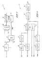
- Figure 1 shows a block diagram of a transmitter comprising, in series, an input stage 1, a modulation stage 2 and a main/transmitter stage 3.
- the input stage 1 has a plurality of amplifiers 4.1 to 4.M inclusive, each of which receives one or more input signals i 1 to i N inclusive and supplies an output signal to a summator 5.
- One output of the summator 5 supplies a modulation signal m and is connected to a modulation input of a frequency modulator 6 of the modulation stage 2.
- Another input of the modulator 6 receives a carrier wave signal from an oscillator 7.
- the output signal of the modulator 6 is amplified by an amplifier 8 of the main/transmitter stage 3 and after amplification is emitted by an antenna 9.
- the frequency modulator comprises, for example, a phase modulator and an integrator.
- the modulation stage may however, more commonly, also comprise a directly modulatable oscillator, for example a voltage controlled oscillator (VCO).
- VCO voltage controlled oscillator
- the summator 5 may comprise a summing amplifier or, in the simplest embodiment, a junction point.
- the bandwidth of the transmission signal emitted by the antenna 9 is approximately equal to twice the sum of the highest frequency of the modulation signal plus the frequency deviation (or frequency swing). The greater the frequency deviation is, the greater the amplitude of the modulation signal is.
- the amplifiers 4.1 to 4.M inclusive are set with gain factors (which, once set, are intended to remain unchanged) in such a way that the greater the amplitude of an output signal of an amplifier 4.i is, the lower a highest frequency with significant amplitude of the output signal of the amplifier 4.i is. In this way, the frequency deviation of the transmission signal will be greater for signals i having lower highest frequencies. Consequently, adaptive control of the frequency deviation is achieved for the purpose of increasing the bandwidth of the transmission signal within a maximum permitted bandwidth. Thus the receiving sensitivity and/or the reception range for the transmitter signal is increased.
- Figure 2 shows a block diagram of another embodiment of an input stage 1' according to the invention, which can be used instead of the input stage of Figure 1.
- the input stage 1' of Figure 2 comprises a summator 10 which receives, continuously or alternating in random sequence, a single input signal or a group of input signals combined from the input signals i 1 to i N inclusive, and which, depending on the circuits supplying these input signals, may comprise a summing amplifier or even a simple junction point.
- An output of the summator 10 supplies an input signal i x to an input of an amplifier 11 having an adjustable gain factor.
- Control inputs of the adjustable amplifier 11 receive, from a memory 12, a data signal DAT for the purpose of adjusting the gain factor of the amplifier 11.
- An output of the adjustable amplifier 11 supplies the modulation signal m.
- the memory 12 is addressed by an address ADR which is supplied by a coder 13 which receives selection signals S 1 to S N inclusive, each of which indicates whether the input signals, or groups thereof, i 1 to i N inclusive are supplied to the summator 10. If the signals S 1 to S N inclusive are not available in the transmitter, they may easily be generated by using a detector, such as the detector 14 of the input signal i 1 , which receives the input signal in question, or the group of input signals in question, and which detects whether the amplitude of the signal(s) is or is not above a certain value.
- the input stage 1' of Figure 2 need only comprise a single amplifier, namely the adjustable amplifier 11.
- the gain factors stored in the memory 12 are easily changed (although this is not shown), for example by replacing the memory by another memory if it is a read-only memory, or by a user from a workstation if the memory 12 is connected to a control system (not shown) of the transmitter.
- Figure 3 shows a block diagram of an input stage 1" for a transmitter of a paging system.
- Three of the abovementioned input signals i 1 to i N inclusive received by the input stage 1" are a speech signal SP, a binary code signal CD and a binary frequency offset modulation signal FOM.
- the code signal CD may contain an identification number assigned to a portable receiver unit of the system.
- the signal FOM is used in systems having more than one transmitter and comprises a signal whose frequency is approximately twice the bit frequency of the code signal CD, which for different transmitters is differently shifted in phase and is superimposed on the code signal CD. The signal FOM therefore does not exist without a signal CD being supplied to the input stage 1".
- Two selection signals of the abovementioned selection signals S 1 to S N inclusive received by the input stage 1" are a speech enabling signal SE and an FOM detection signal FD. If the signal SE is high, this indicates that a speech signal SP is being received. If both SE and FD are low, this indicates that only a code signal CD is being received. If the signal FD is high, this indicates that a code signal CD is being received onto which the signal FOM must be superimposed.
- the signals SP, CD, FOM, SE and FD are available in systems which can be obtained from the applicant.
- the speech signal SP is first fed through a circuit 20 which amplifies higher frequencies more strongly than lower frequencies, or which attenuates lower frequencies more strongly than higher frequencies ("emphasise circuit").
- the output signal of the circuit 20 is fed through a limiting circuit 21 in order to limit its amplitude.
- the output signal of the limiting circuit 21 is supplied to an input of the adjustable amplifier 11.
- the adjustable amplifier 11 at the same time receives, via a low-pass filter 22, the code signal CD.
- the signal FOM is supplied, via a low-pass filter 23 and an amplifier 24, to an input of a summator 25 which receives, at another input, the output signal of the adjustable amplifier 11.
- the output signal of the summator 25 is supplied to a low-pass filter 26 which, at one output, supplies the modulation signal m for the modulator 6 of Figure 1.
- the address supplied to the memory 12 points to a memory location having a first value for the gain factor of an adjustable amplifier 11. If the selection signal SE is low and the selection signal FD is low, that is to say if only a code signal CD is being received, the address supplied to the memory 12 points to a location having a second value for the gain factor. If the selection signal SE is low and the signal FD is high, that is to say if a code signal CD is being received onto which an FOM signal must be superimposed, the address supplied to the memory 12 points to a location having a third value for the gain factor. The memory 12 therefore need contain only three locations having three values for the gain factor.
- the low-pass filter 26 is preferably a 4th order Chebyshev filter having a cut-off frequency of 3 kHz.
- the low-pass filters 22 and 23 are preferably 10th order Bessel filters, which are almost optimally suited for the code signal CD and the FOM signal, respectively, and which have a smaller bandwidth than that of the filter 26.
- the cut-off frequency of the filter 22 is equal to the bit time of a code signal CD having the shortest bit time, and the cut-off frequency of the filter 23 is equal to twice the cut-off frequency of the filter 22.
- a filter of this type in response to pulses having the bit time of the code signal CD or the FOM signal, produces as the output signal a signal having the shape of a raised cosine pulse. To the extent that more successive bits are high or low, the peak or the trough, respectively, becomes wider.
- bit frequencies of 480 bit/s - 4800 bit/s may be used, corresponding to a sine wave fundamental frequency of 240 Hz - 2400 Hz in the case of alternate reception of logical ones and zeros. It is then expedient for the memory 12 to have more than three storage locations and a correspondingly larger address range, which makes it possible to choose code signals CD having different bit frequencies from different gain factors of the amplifier 11, and thus to choose different frequency deviations of the transmitter signal to be emitted by the antenna 9, for the purpose of increasing the receiving sensitivity and/or the reception range for the transmitter signal. If the frequency of the FOM signal then changes, an adjustable amplifier can be used as the amplifier 24, which adjustable amplifier may be of the same type as the amplifier 11 and whose gain factor is controlled in the same way from a memory.
- the definition of "bandwidth" has not been established unambiguously, that it has changed with time, and that it will probably continue to change.
- the power of the emitted transmitter signal in a neighbouring channel must be attenuated by a particular number of dB's with regard to the power in the channel itself, with in addition an upper limit applying to the power in the neighbouring channel.
- the transmitter input stage according to the invention is not restricted to the embodiments shown.
- the memory 12 may, after all, contain a large number of values for the gain factor of the adjustable amplifier 11 for each individual input signal or for each group of received input signals having various highest (permitted) frequencies.
Landscapes
- Engineering & Computer Science (AREA)
- Computer Networks & Wireless Communication (AREA)
- Signal Processing (AREA)
- Transmitters (AREA)
Claims (9)
- Eingangsstufe eines Senders, die eine Kombinationsschaltung (1, 1', 1") aufweist, die eine Vielzahl von Eingängen zum Empfang von verschiedenen Eingangssignalen (i1, ... iN) hat, welche verschiedene Maximalfrequenzen mit signifikanten Amplituden haben, wobei die Kombinationsschaltung (1, 1', 1") die Eingangssignale zu einem Modulationssignal (m) kombiniert, das einem Ausgang der Kombinationsschaltung zugeführt wird, der mit einer Frequenzmodulationsstufe (2) des Senders verbunden werden soll, um für die Erzeugung und Übertragung eines Sendesignals zu sorgen, das eine Bandbreite hat, die wesentlich kleiner als eine oder gleich einer maximal zulässigen Bandbreite ist,
dadurch gekennzeichnet,
daß die Kombinationsschaltung (1, 1', 1") jedes der Eingangssignale (i1, ..., iN) und/oder eine kombinierte Gruppe von Eingangssignalen (i2, i3) in Abhängigkeit von ihrer Anwesenheit und von ihrer höchsten Frequenz auf eine solche Weise verstärkt, daß die Bandbreite des Sendesignals in Richtung der maximal zulässigen Bandbreite vergrößert wird. - Eingangsstufe eines Senders nach Anspruch 1,
dadurch gekennzeichnet,
daß die Kombinationsschaltung (1') einen Verstärker (11) mit einem einstellbaren Verstärkungsfaktor hat, der Eingänge zum Empfang eines einzelnen Eingangssignals (ix) oder einer kombinierten Gruppe von Eingangssignalen der genannten Eingangssignale (i1, ..., iN) hat, wobei die Kombinationsschaltung (1') einen Speicher (12) hat, in dem für jedes einzelne Eingangssignal bzw. für jede Gruppe von Eingangssignalen, die von dem Verstärker (11) zu verstärken sind, ein zugeordneter Verstärkungsfaktor gespeichert ist, der ausgelesen und dem Verstärker (11) zu dem Zweck zugeführt wird, den Verstärkungsfaktor beim Empfang des zugeordneten einzelnen Eingangssignals (ix) bzw. der zugeordneten Gruppe von Eingangssignalen durch den Verstärker (11) einzustellen. - Eingangsstufe eines Senders nach Anspruch 1,
dadurch gekennzeichnet,
daß die Kombinationsschaltung (1") einen Verstärker (11) mit einem einstellbaren Verstärkungsfaktor hat, der Eingänge zum Empfang eines einzelnen Eingangssignals oder einer kombinierten Gruppe von Eingangssignalen der genannten Eingangssignale hat, wobei die Kombinationsschaltung (1") einen Speicher (12) hat, in dem für jedes einzelne Eingangssignal (Sp, CD) bzw. jede Gruppe von Eingangssignalen, die von dem Verstärker (11) zu verstärken sind, ein zugeordneter Verstärkungsfaktor gespeichert ist, der ausgelesen und dem Verstärker (11) zu dem Zweck zugeführt wird, den Verstärkungsfaktor beim Empfang des zugeordneten einzelnen Eingangssignals bzw. der zugeordneten Gruppe von Eingangssignalen durch den Verstärker (11) einzustellen, und wobei die Eingangssignale der Kombinationsschaltung (1") ein Codesignal (CD), ein Frequenzoffset-Modulationssignal (FOM) und ein Sprachsignal (Sp) aufweisen können. - Eingangsstufe eines Senders nach Anspruch 3,
dadurch gekennzeichnet,
daß unterschiedliche Verstärkungsfaktoren Codesignalen (CD) zugeordnet sind, die unterschiedliche Bitdauern haben. - Eingangsstufe eines Senders nach Anspruch 3,
dadurch gekennzeichnet,
daß unterschiedliche Verstärkungsfaktoren unterschiedlichen Gruppen zugeordnet sind, die jeweils ein Codesignal und ein Frequenzoffset-Modulationssignal (FOM) aufweisen, wobei die Gruppen unterschiedliche Bitdauern haben. - Eingangsstufe eines Senders nach Anspruch 3, 4 oder 5,
dadurch gekennzeichnet,
daß das Frequenzoffset-Modulationssignal (FOM) längs eines getrennten Pfades mit einem festgelegten Verstärkungsfaktor verstärkt wird und daß die Kombinationsschaltung (1") eine Summiereinrichtung (25) hat, die an ihren Eingängen ein Ausgangssignal des Verstärkers (11) mit einstellbarem Verstärkungsfaktor und das verstärkte Frequenzoffset-Modulationssignal (FOM) empfängt und an einem Ausgang das Modulationssignal abgibt. - Eingangsstufe eines Senders nach einem der Ansprüche 3 bis 6 einschließlich,
wobei das System geeignet ist, eine Anzeige (SE) zu liefern, die anzeigt, daß ein Eingangssignal ein Sprachsignal (Sp) ist, und eine Anzeige (FD) zu liefern, die anzeigt, daß ein Eingangssignal ein Frequenzoffset-Modulationssignal (FOM) ist, wobei jeder der Verstärkungsfaktoren in einem dem Faktor zugeordneten Register gespeichert ist, und wobei die Kombinationsschaltung (1") eine Logik-Kombinationsschaltung aufweist, die die beiden Anzeigen (SE, FD) empfängt und in Abhängigkeit von den empfangenen Anzeigen eines der Register zu dem Zweck aktiviert, dem Verstärker (11) einen einstellbaren Verstärkungsfaktor der in dem aktivierten Register gespeicherten Verstärkungsfaktoren zuzuführen. - Eingangsstufe eines Senders nach einem der Ansprüche 3 bis 7 einschließlich,
gekennzeichnet durch ein oder mehr Filter (22, 23, 26) zwischen den Eingängen und dem Ausgang der Kombinationsschaltung (1") zu dem Zweck der Begrenzung der Frequenzen der Eingangssignale (Sp, CD, FOM) in dem Modulationssignal (m) auf im wesentlichen eine Höchstfrequenz davon. - Eingangsstufe eines Senders nach Anspruch 8,
dadurch gekennzeichnet,
daß die Höchstfrequenz des Modulationssignals (m) im wesentlichen die höchste zulässige Frequenz des Sprachsignals (Sp) ist.
Applications Claiming Priority (2)
| Application Number | Priority Date | Filing Date | Title |
|---|---|---|---|
| NL9101908 | 1991-11-15 | ||
| NL9101908A NL9101908A (nl) | 1991-11-15 | 1991-11-15 | Zenderingangstrap met adaptieve frequentiedeviatiebesturing. |
Publications (2)
| Publication Number | Publication Date |
|---|---|
| EP0542333A1 EP0542333A1 (de) | 1993-05-19 |
| EP0542333B1 true EP0542333B1 (de) | 1997-03-05 |
Family
ID=19859916
Family Applications (1)
| Application Number | Title | Priority Date | Filing Date |
|---|---|---|---|
| EP19920203235 Expired - Lifetime EP0542333B1 (de) | 1991-11-15 | 1992-10-21 | Sendereingangsstufe mit adaptiver Frequenzhubsteuerung |
Country Status (3)
| Country | Link |
|---|---|
| EP (1) | EP0542333B1 (de) |
| DE (1) | DE69217831T2 (de) |
| NL (1) | NL9101908A (de) |
Families Citing this family (1)
| Publication number | Priority date | Publication date | Assignee | Title |
|---|---|---|---|---|
| IT1305710B1 (it) * | 1998-12-11 | 2001-05-15 | Itelco S P A | Metodo per la trasmissione di piu' segnali di tipo broadcast |
Family Cites Families (4)
| Publication number | Priority date | Publication date | Assignee | Title |
|---|---|---|---|---|
| US3886457A (en) * | 1973-04-02 | 1975-05-27 | Danny A Petaja | Level compensated frequency selector |
| US4363131A (en) * | 1981-03-02 | 1982-12-07 | Ael Microtel, Ltd. | Built-in group delay testing arrangement for an FM radio system |
| US5031230A (en) * | 1988-10-24 | 1991-07-09 | Simulcomm Partnership | Frequency, phase and modulation control system which is especially useful in simulcast transmission systems |
| US4972439A (en) * | 1989-01-19 | 1990-11-20 | Motorola, Inc. | Active signalling transmitter control |
-
1991
- 1991-11-15 NL NL9101908A patent/NL9101908A/nl not_active Application Discontinuation
-
1992
- 1992-10-21 DE DE1992617831 patent/DE69217831T2/de not_active Expired - Fee Related
- 1992-10-21 EP EP19920203235 patent/EP0542333B1/de not_active Expired - Lifetime
Also Published As
| Publication number | Publication date |
|---|---|
| DE69217831T2 (de) | 1997-09-04 |
| NL9101908A (nl) | 1993-06-01 |
| EP0542333A1 (de) | 1993-05-19 |
| DE69217831D1 (de) | 1997-04-10 |
Similar Documents
| Publication | Publication Date | Title |
|---|---|---|
| CA2047870C (en) | Automatic power control apparatus | |
| US4017856A (en) | Self-calibrating microwave transponder | |
| AU630978B2 (en) | Transmitter | |
| US5406584A (en) | Time shift keying digital communications system | |
| EP1216503B1 (de) | Burst-leistungsverstärker mit individuellen rampenprofilen in abhängigkeit des ersten nachrichtensymbols | |
| WO1995012245A1 (en) | Method and apparatus for controlling a peak envelope power of a power amplifier | |
| CA2145652C (en) | Method and apparatus for controlling a peak envelope power of a pa | |
| EP0542333B1 (de) | Sendereingangsstufe mit adaptiver Frequenzhubsteuerung | |
| JPH0677753A (ja) | Alc回路 | |
| JP2000078096A (ja) | 連続タイムスロットにおける伝送方法 | |
| EP0534484A1 (de) | Schaltung für Impulsleistungsverstärker, dessen Ausgangssignal die erwünschte Kurvenform hat | |
| US4748641A (en) | Suppressed carrier modulation method | |
| US7062289B2 (en) | Method and apparatus of multi-carrier power control of base station in broad-band digital mobile communication system | |
| EP1057281B1 (de) | Kompensation von durch taktflattern verursachten phasenfehlern in einem cdma-kommunikationssystem | |
| US5195105A (en) | Spread spectrum receiver | |
| US11619699B2 (en) | AoA/AoD calculation in the presence of carrier frequency offset | |
| US6009119A (en) | Adaptive power leveling of an RF transceiver utilizing information stored in non-volatile memory | |
| US7336726B2 (en) | Apparatus and method for power control in digital mobile communication system broadband multi-carrier base station | |
| CA1221432A (en) | Remote monitoring system transmitter and power supply therefor | |
| FI86933C (fi) | Foerfarande och anordning foer styrning av en radiosaendare | |
| WO1991015911A1 (en) | Communication system | |
| WO1997003500A1 (en) | Pulse width modulation pulse shaper | |
| EP1655853B1 (de) | Verfahren zum Modulieren geformter Impulse | |
| US6590462B1 (en) | Noise code string generator and CN controller comprising it | |
| CN1937411A (zh) | 用于锁相环系统中的信号滤波的系统和方法 |
Legal Events
| Date | Code | Title | Description |
|---|---|---|---|
| PUAI | Public reference made under article 153(3) epc to a published international application that has entered the european phase |
Free format text: ORIGINAL CODE: 0009012 |
|
| AK | Designated contracting states |
Kind code of ref document: A1 Designated state(s): CH DE FR GB LI NL SE |
|
| 17P | Request for examination filed |
Effective date: 19930607 |
|
| 17Q | First examination report despatched |
Effective date: 19950714 |
|
| GRAG | Despatch of communication of intention to grant |
Free format text: ORIGINAL CODE: EPIDOS AGRA |
|
| GRAH | Despatch of communication of intention to grant a patent |
Free format text: ORIGINAL CODE: EPIDOS IGRA |
|
| GRAH | Despatch of communication of intention to grant a patent |
Free format text: ORIGINAL CODE: EPIDOS IGRA |
|
| GRAA | (expected) grant |
Free format text: ORIGINAL CODE: 0009210 |
|
| AK | Designated contracting states |
Kind code of ref document: B1 Designated state(s): CH DE FR GB LI NL SE |
|
| REG | Reference to a national code |
Ref country code: CH Ref legal event code: EP |
|
| REF | Corresponds to: |
Ref document number: 69217831 Country of ref document: DE Date of ref document: 19970410 |
|
| ET | Fr: translation filed | ||
| REG | Reference to a national code |
Ref country code: CH Ref legal event code: NV Representative=s name: BUECHEL, VON REVY & PARTNER |
|
| REG | Reference to a national code |
Ref country code: CH Ref legal event code: AEN Free format text: DAS PATENT IST AUFGRUND DES WEITERBEHANDLUNGSANTRAGS VOM 13.06.1997 REAKTIVIERT WORDEN. |
|
| PLBE | No opposition filed within time limit |
Free format text: ORIGINAL CODE: 0009261 |
|
| 26N | No opposition filed | ||
| NLS | Nl: assignments of ep-patents |
Owner name: TELEFONAKTIEBOLAGET LM ERICSSON |
|
| REG | Reference to a national code |
Ref country code: GB Ref legal event code: 732E |
|
| PGFP | Annual fee paid to national office [announced via postgrant information from national office to epo] |
Ref country code: NL Payment date: 20011031 Year of fee payment: 10 |
|
| REG | Reference to a national code |
Ref country code: FR Ref legal event code: TP |
|
| REG | Reference to a national code |
Ref country code: GB Ref legal event code: IF02 |
|
| REG | Reference to a national code |
Ref country code: CH Ref legal event code: PUE Owner name: ERICSSON RADIO SYSTEMS B.V. TRANSFER- TELEFONAKTIE |
|
| PGFP | Annual fee paid to national office [announced via postgrant information from national office to epo] |
Ref country code: FR Payment date: 20021017 Year of fee payment: 11 Ref country code: CH Payment date: 20021017 Year of fee payment: 11 |
|
| PGFP | Annual fee paid to national office [announced via postgrant information from national office to epo] |
Ref country code: SE Payment date: 20021018 Year of fee payment: 11 Ref country code: GB Payment date: 20021018 Year of fee payment: 11 Ref country code: DE Payment date: 20021018 Year of fee payment: 11 |
|
| PG25 | Lapsed in a contracting state [announced via postgrant information from national office to epo] |
Ref country code: NL Free format text: LAPSE BECAUSE OF NON-PAYMENT OF DUE FEES Effective date: 20030501 |
|
| NLV4 | Nl: lapsed or anulled due to non-payment of the annual fee |
Effective date: 20030501 |
|
| PG25 | Lapsed in a contracting state [announced via postgrant information from national office to epo] |
Ref country code: GB Free format text: LAPSE BECAUSE OF NON-PAYMENT OF DUE FEES Effective date: 20031021 |
|
| PG25 | Lapsed in a contracting state [announced via postgrant information from national office to epo] |
Ref country code: SE Free format text: LAPSE BECAUSE OF NON-PAYMENT OF DUE FEES Effective date: 20031022 |
|
| PG25 | Lapsed in a contracting state [announced via postgrant information from national office to epo] |
Ref country code: LI Free format text: LAPSE BECAUSE OF NON-PAYMENT OF DUE FEES Effective date: 20031031 Ref country code: CH Free format text: LAPSE BECAUSE OF NON-PAYMENT OF DUE FEES Effective date: 20031031 |
|
| PG25 | Lapsed in a contracting state [announced via postgrant information from national office to epo] |
Ref country code: DE Free format text: LAPSE BECAUSE OF NON-PAYMENT OF DUE FEES Effective date: 20040501 |
|
| EUG | Se: european patent has lapsed | ||
| GBPC | Gb: european patent ceased through non-payment of renewal fee |
Effective date: 20031021 |
|
| REG | Reference to a national code |
Ref country code: CH Ref legal event code: PL |
|
| PG25 | Lapsed in a contracting state [announced via postgrant information from national office to epo] |
Ref country code: FR Free format text: LAPSE BECAUSE OF NON-PAYMENT OF DUE FEES Effective date: 20040630 |
|
| REG | Reference to a national code |
Ref country code: FR Ref legal event code: ST |