EP0538428B1 - Process for producing miniaturised chemo and bio-sensor elements with an ion-selective diaphragm and bases for these elements - Google Patents
Process for producing miniaturised chemo and bio-sensor elements with an ion-selective diaphragm and bases for these elements Download PDFInfo
- Publication number
- EP0538428B1 EP0538428B1 EP92909188A EP92909188A EP0538428B1 EP 0538428 B1 EP0538428 B1 EP 0538428B1 EP 92909188 A EP92909188 A EP 92909188A EP 92909188 A EP92909188 A EP 92909188A EP 0538428 B1 EP0538428 B1 EP 0538428B1
- Authority
- EP
- European Patent Office
- Prior art keywords
- containment
- membrane
- layer
- ion
- opening
- Prior art date
- Legal status (The legal status is an assumption and is not a legal conclusion. Google has not performed a legal analysis and makes no representation as to the accuracy of the status listed.)
- Expired - Lifetime
Links
Images


Classifications
-
- G—PHYSICS
- G01—MEASURING; TESTING
- G01N—INVESTIGATING OR ANALYSING MATERIALS BY DETERMINING THEIR CHEMICAL OR PHYSICAL PROPERTIES
- G01N27/00—Investigating or analysing materials by the use of electric, electrochemical, or magnetic means
- G01N27/26—Investigating or analysing materials by the use of electric, electrochemical, or magnetic means by investigating electrochemical variables; by using electrolysis or electrophoresis
- G01N27/403—Cells and electrode assemblies
- G01N27/414—Ion-sensitive or chemical field-effect transistors, i.e. ISFETS or CHEMFETS
Definitions
- the invention relates to a method for producing miniaturized chemical and biosensor elements with ion-selective membranes, as well as carriers for these elements.
- Electrodes ion-selective Electrodes
- ISE ion-selective Electrodes
- liquid membranes are used for this purpose used according to the so-called coated-wire principle (see P. Bergveld, DEVELOPMENT AND APPLICATION OF CHEMICAL SENSORS IN LIQUIDS, book: SENSORS AND SENSORY SYSTEMS FOR ADVANCED RO-BOTS, Springer-Verlag Berlin, Heidelberg, 1988, page 403).
- a thin silver wire is used with a so-called ion-selective Surround the liquid membrane.
- the dimensions are coated wire electrode so small that it can also be how veins or arteries can be inserted.
- Analogous coated-film electrodes can be added to the coated-wire electrodes produce. In the simplest case, these exist from a plastic substrate, which is a thin silver or carries a silver layer coated with silver chloride, which is covered with the ion-selective liquid membrane. Coatedfilm electrodes This type can be used instead of plastic also produce on silicon substrates.
- Such liquid membranes are e.g. made of a PVC matrix, which in addition to a plasticizer also contains electroactive substance (ionophore), which the ion selectivity of the membrane. That in a solvent dissolved membrane material can be used to cast membranes be, whereby the solvent evaporates and a solidified membrane is created. From the customer information from FLUKA Feinchemialen GmbH, Neu-Ulm, with the title “Selectophore - Ionophores for Ion-Selective Electrodes" examples can be seen.
- a disadvantage of the known microsensors based on the coated wire principle is that that the membrane is very bad on the wire the coated wire electrode or on the silver layer of the coated film electrode liable. In addition to the poor membrane adhesion these electrodes have the disadvantage that it is due to an ionophore bleeding to depletion of the ionophore comes in the membrane. This not only has the loss of electrochemical properties, but because of the levy substances may also have a biocompatibility restriction when used in the medical field Episode.
- GB-A-2 236 903 is a sensor with an ion selective Membrane known, the base part constructed as an FET sensor is. In addition, support is required. The transistor must be in a watertight position be installed and fitted exactly as it is on the back Lid acts. Filling with a membrane liquid is difficult because only filled from the smaller opening can be.
- An ion-selective membrane can be placed in these supports create a vertical containment that has an opening to the back of the chip has the following properties is characterized: good fillability, micromechanical Anchoring and good lateral microstructures of the Membrane due to the special containment geometry, lower Quotient of active membrane surface and membrane volume to achieve a depot effect, d. H. to minimize ionophore depletion in the membrane, active membrane surface on the back of the silicon chip to ensure optimal contacting and encapsulation conditions.
- the containment itself can be in the silicon substrate with the help known methods of micromechanics, e.g. B. by anisotropic Etching.
- Anisotropic etching is understood to mean a process in which with the help of known lithography and masking techniques Wells or holes z. B. in a (100) -oriented Silicon single crystal wafers are etched. Because of the fourfold Symmetry and the 54.75 ° inclined (111) faces there are pyramidal depressions or holes. The final dimensions of the exit openings depend both of the mask structure, the wafer thickness as well from a precise knowledge of the etching rate in the (111) direction. In this way, arrangements can also be made on a wafer from different wells. It is referenced to the writing by Anton Heuberger, MIKROMECHANIK, Springer-Verlag Berlin, 1989. The with the help of the anisotropic The resulting recess has a pyramid shape and thus a large opening on one wafer surface and with throughputs up to the other surface there a relative small opening.
- Containments with a smaller space requirement can be realized on (110) -oriented silicon substrates. Due to the two-fold symmetry in these substrates, the shapes of the possible containments are more complicated. With a suitable adjustment of the etching masks with respect to the substrate orientation, some of the etching-limiting (111) crystal surfaces and thus also the etching pit side surfaces run vertically, while others are inclined at an angle of 35 ° with respect to the substrate surface (cf. A. Heuberger, loc. Cit., Pp. 344 to 348 and 392 to 397). Since the parallel vertical etching pit walls can be produced with very small distances d p ( ⁇ m range), the containments now result in a much lower chip area consumption. This area consumption is determined by the smallest distance d p mentioned and the etching pit width perpendicular to it, which is given by the inclined pit walls.
- Openings with a very small size tolerance precede the Si wafers anisotropic etching with a so-called etch stop layer on the second wafer surface and up to this First etch the surface and then the etch stop layer in the area of the opening narrowing to the other wafer surface, z. B. from the back to open.
- This is also done by known methods, for example through another selective lithography and etching mask process as well as another etching process.
- SiO 2 layers mentioned instead of the SiO 2 layers mentioned, other materials (for example Si 3 N 4 , Al 2 O 3 , Ta 2 O 5 layers, as well as Al, B, Na-Al and other silicates can also be used , Sol-gel layers but also other suitable materials) occur. It is also possible to supplement the SiO 2 layers with one of the layers mentioned, so that a layer sequence is created, for example SiO 2 and Si 2 N 4 .
- Containments of the type described above have the special one Advantage that due to their special geometry, the membranes in them are micromechanically anchored and the bleeding mobile membrane components (e.g. ionophore, plasticizer) due to the very small in relation to the membrane volume active membrane surface is minimal.
- the bleeding mobile membrane components e.g. ionophore, plasticizer
- the particular advantage of the method is that it is in the processing well-known and sophisticated techniques of microchips can be accessed to the described containments manufacture.
- the membrane stands with a silver layer or a silver layer coated with silver chloride, the parts of the containment inner wall covered, in direct contact.
- the above silver layer can also be made by other suitable ones electrically conductive layers are replaced.
- VISFET vertical ion-selective field effect transistor
- the invention expressly relates to a vertical ISFET (VISFET), which has a vertical containment an ion-selective membrane that has its active membrane surface on the back of the chip.
- VISFET vertical ISFET
- the introduction of the polymer membrane, the liquid membrane or other electrochemically relevant coating materials (e.g. hydrogel) made from the liquid phase can with the help of an automatic microdosing device respectively.
- a material-specific storage time evaporates Solvent and it forms the solidified in the containment ion-selective liquid membrane. If an additional solid electrolyte is used, this can over the membrane as another layer in the same way be applied from the liquid phase.
- ion-selective membranes that are in the containments with a protective layer (e.g. Silicone or epoxy layers). This can for each containment individually but also for the whole Chip or happen for the wafer as a whole.
- a protective layer e.g. Silicone or epoxy layers.
- Ion-selective sensor elements of the type described above can also be designed as biosensor elements.
- this membrane can contain antibodies, microorganisms or organelles wear. In the simplest case, these substances are before Filling the containment already added to the membrane liquid.
- the sensor elements described above can be separated the chips of a wafer built into the housing or with Plastic material are encased. It is special here advantageous that the active membrane surfaces not on the same chip side as the sensitive semiconductor electronics as well as the fine bond wires.
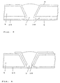
- FIG. 1 shows a section of a section through one that is not part of the invention Sensor chip element, which is in a silicon wafer crystal will be produced.
- t 0.1 mm - 1 mm, preferably 100 ⁇ m - 500 ⁇ m.
- the Containment 2 etched a funnel with the wedge angle of 54.75 ° along the (111) direction.
- the Etching process starts from one surface 3 and sets progresses to the opposite parallel second Surface 4. In the following, the Surface 3 as the front and surface 4 as the back be designated.
- the silicon chip runs parallel to the vertical Walls of the containment.
- two openings 5 and 6 penetrate the front or rear 3 and 4, the diameters of which are related to one another in the manner indicated above.
- the small opening has a diameter between 10 -4 and 10 -1 mm.
- KOH or other known media can be used (cf. A. Heuberger, op. cit., page 125 to 1609).
- All or part of the silicon surface can be etched after the containment z. B. using the known methods of thermal oxidation, the CVD or spin-on-glass technology with a SiO 2 layer 15 which can be silanized for the reason given above. This layer also covers the inner wall of the containment. It is also possible, instead of or additionally, to apply other layers (for example Si 3 N 4 layer) over the SiO 2 layer, likewise by the abovementioned methods.
- other layers for example Si 3 N 4 layer
- the one provided with, usually many containments 2 Wafer is then z. B. on an annular base placed so that the openings of the containments remain free. But it is also possible to polish the wafer on a flat surface Lay plate. With the help of an automatic microdosing device (not shown) the recess 2 filled with a solution forming an ISE membrane. Becomes the lower opening of the Containments left open, so the solution remains due their surface tension and the very small width of the Opening nevertheless in the containment. As is known, it can in such solutions to produce an ion-selective Membrane z. B. PVC, a plasticizer and an ionophore act, dissolved in tetrahydrofuran as a solvent are. Precise recipes for the manufacture of the membrane and Such solutions are the customer information mentioned at the beginning from the company FLUKA. But others can too Membrane materials that are made from the liquid phase leave, as well as other layers (e.g. hydrogel) filled become.
- the opening 5 remains open after filling the solution.
- the wafer provided with the depressions becomes dust-free Atmosphere until the solvent evaporates is and a solidified membrane 7 is formed Has.
- the active membrane surface is which fills the opening 6, very small while the entire membrane volume is very large. It follows thus also a low ionophore depletion over time in the membrane 7.
- FIG. Another embodiment not belonging to the invention is shown in FIG.
- a protective layer 30 z. B. epoxy or Silicon layer
- FIG. 3 shows an exemplary embodiment not belonging to the invention, from which the possibility emerges of the containment geometry in the Area of the small opening on the back of the chip with the help an etch stop layer 18 to be set exactly.
- the etching process automatically on a previously B. heavily doped with boron Etching stop layer interrupted (see: A. Heuberger, a. a. O., Pages 151 and 141 to 1459).
- the small opening of the containment z. B. from the back be opened. Filling and covering the membrane can then be done in the same way as in the previous Examples are given.
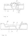
- FIG. 4 shows one possibility of using the containment described above for the production of sensor elements according to the modified coated-film principle.
- the wafer 1 which is provided with an insulating and possibly silanized SiO 2 layer or another insulating layer, is also provided with a thin metal film 16, which is formed in the shape of a funnel or strip in the region of the depression and which, for. B. is applied using known mask technology and vapor deposition or sputtering.
- the metal film which consists for example of silver, a silver layer coated with silver chloride or another electrically conductive layer (e.g. platinum or gold), serves to establish an electrical connection between the membrane 7 introduced later and one on the same silicon chip integrated signal electronics (not shown).
- Chloridation of the vapor-deposited or sputtered Silver layer can e.g. B. according to the known methods by chemical or galvanic means.
- a silicon single crystal wafer is described in the Etched anisotropically (see FIG. 5), with one Indentation 2 shows that when using (100) -oriented Silicon the shape of an inverse truncated pyramid Has. If (110) oriented silicon is used, then so Forms are obtained with a suitable adjustment of the etching masks the recess 2, which is divided by two parallel vertical and two sloping walls. Because of the possible short distance between the parallel vertical containment walls can sensor elements with very low Chip space consumption can be realized. In this 5 shows a section through the sensor element that is parallel to the vertical containment walls runs.
- the containment is produced in a substrate 1 which previously analogous to VMOS-FET (see R. Paul, op. cit., page 336) with a heavily N-doped source layer 22, a P-doped Layer 21 for the channel area and an n-doped Drain layer 23 is provided.
- the drain area can, as shown in Figure 5, through the silicon substrate 1 itself. But it is also possible, analogous to VMOS-FET to use an additional layer that is epitaxial can be generated on the substrate. Subsequently becomes a solution forming the ISE membrane in the recess 2 filled and until the solvent evaporates and formation of the membrane 7 left.
- the channel area is located in the area of the larger opening 5.
- a layer structure such that the channel area 21 is located in the area of the smaller opening 6.
- the gate dielectric consists, as in the known ISFET z. B. from SiO 2 or a SiO 2 / Si 3 N 4 layer sequence.
- the large opening of the containment can be after the ion selective Membrane is formed, as shown in Fig. 2, be covered with a protective layer.
- the membrane 7 forms the so-called "gate” of the VIS-FET. It is expressly noted that in addition to the present one “Depletion type” also the so-called “enrichment type” as well as ISFET with reversed line types (n and p interchanged) can be provided.
- FIGS. 5 and 6 are also suitable for the production of VISFET with a solid-state membrane and an additional electrochemically relevant layer 7 which replaces the liquid membrane.
- the dielectric layer 15 can thus be formed on the silicon as a result of an SiO 2 layer and an additional solid layer (eg Si 3 N 4 , Ta 2 O 5 or the like).
- This additional layer can, for. B. on the SiO 2 using the known CVD, sputtering or sol-gel technology and serves as an ion-selective solid membrane.
- This layer can be made of hydrogel, for example exist that the electrochemical response of the underlying Solid-state membrane extremely delayed, so that by combining the VISFET structures with and without a hydrogel layer 7 the known possibility for differential measurement results.
- the ion-selective sensor elements shown above with Micromechanically structured containment can also do so be modified so that they have a solidified inner electrolyte layer work according to the half-cell principle.
- Figures 7 and 8 show two embodiments.
- the example 7 differs from FIG. 4 only in that that the lead electrode 16 is not so deep in the containment reaches in and over the ion-selective liquid membrane 7, a solidified inner electrolyte layer 31 is arranged is.
- the lead electrode can e.g. B. from one with Silver chloride coated silver film exist.
- the ion-selective liquid membrane e.g. PVC membrane
- the internal electrolyte is poured in a further casting process.
- the inner electrolyte can be made in a known manner Saline solution (z. B. KCl) exist, the z. B. with gelatin, agar or polyvinyl alcohol is added, so that some Time after filling the initially liquid internal electrolyte a solidified inner electrolyte layer in the containment above the ion-selective liquid membrane.
- a further variant is shown in FIG differs from the previous one in that the large containment 2 is a small containment 32, that is directly connected to the big one and also itself by the anisotropic etching method described above can generate.
- This structure facilitates the separation from Liquid membrane and inner electrolyte layer.
- VISFET structures with an internal electrolyte can also be used produce ( Figure 9).
- This embodiment differs from the example according to FIG. 5 in that that over the dielectric layer 15 z.
- B. a silver layer 33 evaporated or sputtered and lithographically is structured with a layer of silver chloride is covered.
- the containment becomes analogous, for example from Figure 8 with liquid membrane 7 and internal electrolyte 31 provided.
- capillary channels can be V-shaped or Have U-shaped cross sections.
- FIG. 10 shows a structure according to FIG. 4 as an example on average with a capillary channel 34 and a Filling opening 35 is provided.
- the membrane fluid will filled into the large filling opening. It is due to the Capillary forces in the channel promoted and then fills that Containment. It is also possible from a filling opening from several containments on surrounding chips or on to fill all chips of a wafer with membrane liquid. The filler opening can then be separated Chips of a wafer are separated. To improve the Flow behavior of the membrane solution can be filled under Solvent atmosphere take place.
- FIG. 11 shows a system of capillary channels 34 and large filling openings 35 shown.
- a chip 39 At the end of each Capillary channel is a chip 39 and the containment 2 of a sensor element.
- FIG. 12 shows a silicon chip with an ion-selective one Membrane 7 in a containment containing its active membrane surface on which the back of the chip has 4.
- On the front of the chip 3 are the contact surfaces of the chip, that with the help of fine bond wires 36 with the housing contacts get connected.
- a carrier 38 and the whole Sensor chip sealed on the front with plastic become.
Abstract
Description
Die Erfindung betrifft ein Verfahren zur Herstellung von miniaturisierten Chemo- und Biosensorelementen mit ionenselektiven Membranen, sowie von Trägern für diese Elemente.The invention relates to a method for producing miniaturized chemical and biosensor elements with ion-selective membranes, as well as carriers for these elements.
Es ist bekannt, Mikrosensoren, die nach dem Prinzip der ionenselektiven Elektroden (ISE) ohne flüssigen Innenelektrolyten arbeiten, in sehr kleinen Ausführungen herzustellen. Hierzu werden beispielsweise Elektroden mit Flüssigmembranen nach dem sogenannten coated-wire-Prinzip eingesetzt (vgl. P. Bergveld, DEVELOPMENT AND APPLICATION OF CHEMICAL SENSORS IN LIQUIDS, Buch: SENSORS AND SENSORY SYSTEMS FOR ADVANCED RO-BOTS, Springer-Verlag Berlin, Heidelberg, 1988, Seite 403). Ein dünner Silberdraht wird mit einer sogenannten ionenselektiven Flüssigmembran umgeben. Von den Dimensionen ist die coated-wire-Elektrode so klein, daß sie auch in Körpergefäße, wie Venen oder Arterien eingeführt werden kann. Analog zu den coated-wire-Elektroden lassen sich coated-film-Elektroden herstellen. Im einfachsten Fall bestehen diese aus einem Kunststoffsubstrat, das eine dünne Silber- bzw. eine mit Silberchlorid überzogene Silberschicht trägt, die mit der ionenselektiven Flüssigmembran bedeckt ist. Coatedfilm-Elektroden dieser Art lassen sich anstelle von Kunststoff- auch auf Siliziumsubstraten herstellen.It is known to use microsensors based on the principle of ion-selective Electrodes (ISE) without liquid internal electrolytes work in very small versions. For example, electrodes with liquid membranes are used for this purpose used according to the so-called coated-wire principle (see P. Bergveld, DEVELOPMENT AND APPLICATION OF CHEMICAL SENSORS IN LIQUIDS, book: SENSORS AND SENSORY SYSTEMS FOR ADVANCED RO-BOTS, Springer-Verlag Berlin, Heidelberg, 1988, page 403). A thin silver wire is used with a so-called ion-selective Surround the liquid membrane. The dimensions are coated wire electrode so small that it can also be how veins or arteries can be inserted. Analogous coated-film electrodes can be added to the coated-wire electrodes produce. In the simplest case, these exist from a plastic substrate, which is a thin silver or carries a silver layer coated with silver chloride, which is covered with the ion-selective liquid membrane. Coatedfilm electrodes This type can be used instead of plastic also produce on silicon substrates.
Auch ist die Herstellung von ionenselektiven Flüsszgmembranen an sich bekannt. Solche Flüssigmembranen bestehen z.B. aus einer PVC-Matrix, die neben einem Weichmacher auch eine elektroaktive Substanz (Ionophor) enthält, die die Ionenselektivität der Membran bestimmt. Das in einem Lösungsmittel gelöste Membranmaterial kann zum Gießen von Membranen verwendet werden, wobei sich das Lösungsmittel verflüchtigt und eine verfestigte Membran entsteht. Aus der Kundeninformation der Firma FLUKA Feinchemikalien GmbH, Neu-Ulm, mit dem Titel "Selectophore - Ionophores for Ion-Selective Electrodes" sind Beispiele ersichtlich.Also is the manufacture of ion selective liquid membranes known per se. Such liquid membranes are e.g. made of a PVC matrix, which in addition to a plasticizer also contains electroactive substance (ionophore), which the ion selectivity of the membrane. That in a solvent dissolved membrane material can be used to cast membranes be, whereby the solvent evaporates and a solidified membrane is created. From the customer information from FLUKA Feinchemialen GmbH, Neu-Ulm, with the title "Selectophore - Ionophores for Ion-Selective Electrodes" examples can be seen.
Nachteilig ist bei den bekannten Mikrosensoren nach dem coated-wire-Prinzip, daß die Membran sehr schlecht an dem Draht der coated-wire-Elektrode bzw. an der Silberschicht der coated-film-Elektrode haftet. Neben der schlechten Membranhaftung haben diese Elektroden den Nachteil, daß es aufgrund einer Ionophor-Ausblutung zu einer Verarmung des Ionophors in der Membran kommt. Dies hat nicht nur den Verlust der elektrochemischen Eigenschaften, sondern wegen der Abgabe von Stoffen unter Umständen auch eine Einschränkung der Biokompatibilität beim Einsatz im medizinischen Bereich zur Folge.A disadvantage of the known microsensors based on the coated wire principle is that that the membrane is very bad on the wire the coated wire electrode or on the silver layer of the coated film electrode liable. In addition to the poor membrane adhesion these electrodes have the disadvantage that it is due to an ionophore bleeding to depletion of the ionophore comes in the membrane. This not only has the loss of electrochemical properties, but because of the levy substances may also have a biocompatibility restriction when used in the medical field Episode.
Die beiden oben genannten Probleme treten auch bei der Anwendung
ionenselektiver Flüssigmembranen in Gatebereich ionenselektiver
Feldeffekttransistoren (ISFET) auf. Für die
Lösung des Haftungsproblems wurden in der Literatur Polyimid-Haltenetze
sowie anisotrop geätzte Silizium-Deckel mit
enger Öffnung angegeben (vergleiche hierzu Kapitel 4 des Buches
"Sensors" von W. Göpel, J. Hesse, J. N. Zemel (Ed.),
Band 1, VCH Verlagsgesellschaft Weinheim, 1989, Seite 97 bis
99). Das dort besprochene Haltenetz löst die gestellte Aufgabe
nur hinsichtlich der Membranhaftung. Die Anwendung eines
Siliziumdeckels stellt ein sehr aufwendiges Verfahren
dar, das aufgrund der Justierprobleme bei der Deckelmontage
auf relativ großflächige Strukturen (0,1 mm-Strukturen) beschränkt
bleiben muß.The above two problems also occur during application
ion-selective liquid membranes in the gate area
Field effect transistors (ISFET). For the
In the literature, polyimide holding nets have been used to solve the liability problem
as well as anisotropically etched silicon lids
narrow opening (see
Aus der GB-A-2 236 903 ist ein Sensor mit einer ionenselektiven Membran bekannt, dessen Basisteil als FET-Sensor aufgebaut ist. Zusätzlich ist allerdings ein Support erforderlich. Der Transistor muß in einer wasserdichten Position eingebaut und genau eingepaßt sein, da er als rückseitiger Deckel fungiert. Die Befüllung mit einer Membranflüssigkeit ist schwierig, da nur von der kleineren Öffnung aus befüllt werden kann.From GB-A-2 236 903 is a sensor with an ion selective Membrane known, the base part constructed as an FET sensor is. In addition, support is required. The transistor must be in a watertight position be installed and fitted exactly as it is on the back Lid acts. Filling with a membrane liquid is difficult because only filled from the smaller opening can be.
Bei der Integration von ionenselektiven Sensorelementen auf einem integrierten Schaltkreis ergeben sich zusätzliche Verkapselungsprobleme, da aufgrund der geringen Abmessungen solcher Silizium-Chips die aktive Membranoberfläche in unmittelbarer Nachbarschaft der dünnen Bonddrähte liegt, die den Chip mit den Anschlußkontakten des Sensorgehäuses elektrisch verbinden.When integrating ion-selective sensor elements an integrated circuit results in additional encapsulation problems, because of the small dimensions such silicon chips the active membrane surface in immediate Neighborhood of the thin bond wires lies that the chip with the contacts of the sensor housing electrically connect.
Zur Lösung des letztgenannten Problems wurde in der Literatur ISFET-Strukturen mit Rückseitenkontakten angegeben (vgl. z. B.: D. Ewald, A. van den Berg and A. Grisel: "Technology for Backside Contacted pH-sensitive ISFETs Embedded in a p-Well Structurea, in der Zeitschrift Sensors and Actuators, B1 (1990), p. 335 - 340).To solve the latter problem has been found in the literature ISFET structures with rear contacts specified (cf. z. E.g .: D. Ewald, A. van den Berg and A. Grisel: "Technology for Backside Contacted pH-sensitive ISFETs Embedded in a p-Well Structurea, in the journal Sensors and Actuators, B1 (1990), p. 335-340).
Als Nachteil solcher Lösungen ist die Tatsache anzusehen, daß die Chip-Oberfläche mit den empfindlichen Halbleiterstrukturen der Signalelektronik nur durch eine dünne Passivierungsschicht vom flüssigen Meßmedium getrennt ist. Schon sehr geringe Verunreinigungen der Halbleiterstrukturen machen die Meßelektronik unbrauchbar. Insbesondere das letztgenannte Verkapselungsproblem tritt nicht nur bei ionenselektiven Sensorelementen mit Flüssigmembranen, sondern auch bei solchen mit anderen, z. B. Festkörpermembranen auf, die Teil eines integrierten Schaltkreises sind.The disadvantage of such solutions is the fact that the chip surface with the sensitive semiconductor structures the signal electronics only through a thin passivation layer is separated from the liquid measuring medium. Nice make very little contamination of the semiconductor structures the measuring electronics unusable. In particular the latter Encapsulation problem does not only occur with ion-selective Sensor elements with liquid membranes, but also in those with others, e.g. B. solid membranes on the Are part of an integrated circuit.
Für eine Verbesserung kommt es also wesentlich darauf an, ein Prinzip anzugeben, das es erlaubt, ionenselektive Sensorelemente auf Silizium-Chips zu realisieren, die mit Flüssigmembranen, aber auch mit anderen Membranen bzw. elektrochemisch oder biochemisch relevanten Sensorelementbeschichtungen arbeiten, die aus flüssiger Phase hergestellt werden und folgende Eigenschaften aufweisen: gute Membranhaftung, minimale Ionophorverarmung in der Flüssigmembran, gute Aufbringungsmöglichkeiten und Mikrostrukturierbarkeit von Membranen auf Siliziumoberflächen ohne zusätzliche Feinbearbeitung von Verschlußteilen, hohe elektrische Stabilität, gute Bedingungen für die Kontaktierung und Verkapselung des Sensor-Chips.For an improvement, it is essential that to specify a principle that allows ion-selective sensor elements to realize on silicon chips that with liquid membranes, but also with other membranes or electrochemically or biochemically relevant sensor element coatings work that are made from the liquid phase and have the following properties: good membrane adhesion, minimal depletion of ionophore in the liquid membrane, good application possibilities and microstructurability of membranes on silicon surfaces without additional finishing of fastener parts, high electrical stability, good Conditions for contacting and encapsulating the sensor chip.
Diese Aufgabe wird gelöst durch Einsatz von Trägern, die
nach dem Verfahren des Anspruches 1 hergestellt sind.This task is solved by using carriers that
are produced by the method of
In diesen Trägern läßt sich eine ionenselektive Membran in einem vertikalen Containment herstellen, das eine Öffnung zur Chip-Rückseite besitzt und das durch folgende Eigenschaften gekennzeichnet ist: gute Befüllbarkeit, mikromechanische Verankerung sowie gute laterale Mikrostrukturen der Membran aufgrund der speziellen Containmentgeometrie, niedriger Quotient aus aktiver Membranoberfläche und Membranvolumen zur Erzielung eines Depot-Effektes, d. h. zur Minimierung der Ionophorverarmung in der Membran, aktive Membranoberfläche auf der Rückseite des Silizium-Chips zur Gewährleistung optimaler Kontaktierungs- und Verkapselungsbedingungen.An ion-selective membrane can be placed in these supports create a vertical containment that has an opening to the back of the chip has the following properties is characterized: good fillability, micromechanical Anchoring and good lateral microstructures of the Membrane due to the special containment geometry, lower Quotient of active membrane surface and membrane volume to achieve a depot effect, d. H. to minimize ionophore depletion in the membrane, active membrane surface on the back of the silicon chip to ensure optimal contacting and encapsulation conditions.
Das Containment selbst kann im Siliziumsubstrat mit Hilfe bekannter Verfahren der Mikromechanik, z. B. durch anisotropes Ätzen hergestellt werden.The containment itself can be in the silicon substrate with the help known methods of micromechanics, e.g. B. by anisotropic Etching.
Unter anisotropem Ätzen wird ein Verfahren verstanden, bei dem mit Hilfe bekannter Lithographie- und Maskentechniken Vertiefungen oder Löcher z. B. in einen (100)-orientierten Silizium-Einkristall-Wafer geätzt werden. Wegen der vierzähligen Symmetrie und den jeweils um 54,75° geneigten (111)-Flächen ergeben sich pyramidenförmige Vertiefungen bzw. Löcher. Die endgültigen Abmessungen der Ausgangsöffnungen hängen sowohl von der Maskenstruktur, der Wafer-Dicke als auch von einer genauen Kenntnis der Ätzrate in (111)-Richtung ab. Auf diese Weise lassen sich auch auf einem Wafer Anordnungen von unterschiedlichen Vertiefungen herstellen. Es wird verwiesen auf die Schrift von Anton Heuberger, MIKROMECHANIK, Springer-Verlag Berlin, 1989. Die mit Hilfe des anisotropen Ätzens sich ergebende Vertiefung hat eine Pyramidenform und damit eine große Öffnung auf der einen Wafer-Oberfläche und bei Durchätzen bis zur anderen Oberfläche dort eine relativ kleine Öffnung. Anisotropic etching is understood to mean a process in which with the help of known lithography and masking techniques Wells or holes z. B. in a (100) -oriented Silicon single crystal wafers are etched. Because of the fourfold Symmetry and the 54.75 ° inclined (111) faces there are pyramidal depressions or holes. The final dimensions of the exit openings depend both of the mask structure, the wafer thickness as well from a precise knowledge of the etching rate in the (111) direction. In this way, arrangements can also be made on a wafer from different wells. It is referenced to the writing by Anton Heuberger, MIKROMECHANIK, Springer-Verlag Berlin, 1989. The with the help of the anisotropic The resulting recess has a pyramid shape and thus a large opening on one wafer surface and with throughputs up to the other surface there a relative small opening.
Zwischen dem Durchmesser Wk der kleinen Öffnung und dem
Durchmesser Wg der großen Öffnung besteht für (100)-orientierte
Siliziumsubstrate mit der Dicke t folgender Zusammenhang
(vgl. A. Heuberger, a. a. O., Seite 393):
Hier zeigt sich, daß bei typischen Größen (z. B. von 1 µm bis 100 µm) für die kleine Öffnung ein relativ großer Bedarf an Chipfläche mit dem Durchmesser Wg pro Sensorelement besteht. Somit eignen sich (100)-orientierte Siliziumsubstrate nur für die Realisierung einer begrenzten Anzahl von V-förmigen Containments der oben beschriebenen Art.This shows that with typical sizes (for example from 1 μm to 100 μm) for the small opening there is a relatively large need for chip area with the diameter W g per sensor element. Thus, (100) -oriented silicon substrates are only suitable for the realization of a limited number of V-shaped containments of the type described above.
Containments mit einem geringeren Flächenbedarf lassen sich auf (110)-orientierten Siliziumsubstraten realisieren. Aufgrund der zweizähligen Symmetrie in diesen Substraten sind die Formen der möglichen Containments komplizierter. Hier verlaufen bei einer geeigneten Justierung der Ätzmasken gegenüber der Substratorientierung einige der ätzbegrenzenden (111)-Kristallflächen und damit auch die Ätzgrubenseitenflächen senkrecht, während andere mit einem Winkel von 35° gegenüber der Substratoberfläche geneigt sind (vgl. A. Heuberger, a. a. O., S. 344 bis 348 und 392 bis 397). Da die parallelen senkrechten Ätzgrubenwände mit sehr geringen Abständen dp (µm-Bereich) hergestellt werden können, ergibt sich nun ein sehr viel geringerer Chip-Flächenverbrauch durch die Containments. Dieser Flächenverbrauch wird durch den genannten geringsten Abstand dp sowie die Ätzgrubenweite senkrecht dazu, die durch die geneigten Grubenwände gegeben ist, bestimmt.Containments with a smaller space requirement can be realized on (110) -oriented silicon substrates. Due to the two-fold symmetry in these substrates, the shapes of the possible containments are more complicated. With a suitable adjustment of the etching masks with respect to the substrate orientation, some of the etching-limiting (111) crystal surfaces and thus also the etching pit side surfaces run vertically, while others are inclined at an angle of 35 ° with respect to the substrate surface (cf. A. Heuberger, loc. Cit., Pp. 344 to 348 and 392 to 397). Since the parallel vertical etching pit walls can be produced with very small distances d p (µm range), the containments now result in a much lower chip area consumption. This area consumption is determined by the smallest distance d p mentioned and the etching pit width perpendicular to it, which is given by the inclined pit walls.
Es ist auch möglich, zur Erzielung von durchgeätzen kleinen Öffnungen mit sehr geringer Größentoleranz die Si-Wafer vor dem anisotropen Ätzen mit einer sogenannten Ätzstop-Schicht auf der zweiten Wafer-Oberfläche zu versehen und bis zu dieser Fläche zunächst zu ätzen und anschließend die Ätzstop-Schicht im Bereich der Öffnungsverengung bis zur anderen Wafer-Oberfläche, z. B. von der Rückseite her, zu öffnen. Dies geschieht auch durch bekannte Verfahren, beispielsweise durch einen weiteren selektiven Lithographie- und Ätzmaskenprozeß sowie einen weiteren Ätzvorgang.It is also possible to get through-etched small ones Openings with a very small size tolerance precede the Si wafers anisotropic etching with a so-called etch stop layer on the second wafer surface and up to this First etch the surface and then the etch stop layer in the area of the opening narrowing to the other wafer surface, z. B. from the back to open. This is also done by known methods, for example through another selective lithography and etching mask process as well as another etching process.
Weiterhin ist möglich, mit bekannten Verfahren der thermischen Oxidation, der CVD-, Sputter- oder Sol-Gel-Technik die mit Vertiefungen versehenen Wafer auf der ersten oder zweiten Oberfläche wenigstens im Bereich der Öffnungen der Vertiefung sowie die Innenflächen der Vertiefung mit einer durchgehenden, nichtleitenden SiO2- Schicht zu versehen. Da es aufgrund der hohen Dichte von Hydroxylgruppen an SiO2-Oberflachen zu einer Abstoßung von Flüssigmembranen (z.B. PVC-Membranen) kommt, ist es zur Gewährleistung einer guten Membranhaftung vorteilhaft, diese SiO2-Grenzflächen zu silanisieren. Dieser Silanisierungsprozeß ist im Bereich der Flüssigmembrantechnologie für miniaturisierte Glaselektroden gut eingeführt (vgl. hierzu: Daniel Ammann, "Ion-Selective Microelectrodes", Springer-Verlag, Berlin, 1986). An die Stelle der genannten SiO2-Schichten Können auch andere Materialien (z. B. Si3N4, Al2O3-, Ta2O5-Schichten, sowie Al-, B-, Na-Al- und andere Silikate, Sol-Gel-Schichten aber auch andere geeignete Materialien) treten. Ebenso ist es möglich, die SiO2-Schichten durch eine der genannten Schichten zu ergänzen, so daß eine Schichtenfolge entsteht, z.B. SiO2 und Si2N4.It is also possible, using known methods of thermal oxidation, CVD, sputtering or sol-gel technology, to provide the wafers provided with depressions on the first or second surface at least in the region of the openings in the depression and the inner surfaces of the depression with a continuous, non-conductive SiO 2 layer. Since the high density of hydroxyl groups on SiO 2 surfaces leads to repulsion of liquid membranes (eg PVC membranes), it is advantageous to silanize these SiO 2 interfaces to ensure good membrane adhesion. This silanization process is well established in the field of liquid membrane technology for miniaturized glass electrodes (see: Daniel Ammann, "Ion-Selective Microelectrodes", Springer-Verlag, Berlin, 1986). Instead of the SiO 2 layers mentioned, other materials (for example Si 3 N 4 , Al 2 O 3 , Ta 2 O 5 layers, as well as Al, B, Na-Al and other silicates can also be used , Sol-gel layers but also other suitable materials) occur. It is also possible to supplement the SiO 2 layers with one of the layers mentioned, so that a layer sequence is created, for example SiO 2 and Si 2 N 4 .
Containments der oben beschriebenen Art haben den besonderen Vorteil, daß aufgrund ihrer speziellen Geometrie die Membranen in ihnen mikromechanisch verankert sind und das Ausbluten mobiler Membrankomponenten (z. B. Ionophor, Weichmacher) aufgrund der im Verhältnis zum Membranvolumen sehr geringen aktiven Membranoberfläche minimal ist.Containments of the type described above have the special one Advantage that due to their special geometry, the membranes in them are micromechanically anchored and the bleeding mobile membrane components (e.g. ionophore, plasticizer) due to the very small in relation to the membrane volume active membrane surface is minimal.
Der besondere Vorteil des Verfahrens ist, daß auf in der Bearbeitung von Mikrochips bekannte und ausgereifte Techniken zurückgegriffen werden kann, um die beschriebenen Containments herzustellen.The particular advantage of the method is that it is in the processing well-known and sophisticated techniques of microchips can be accessed to the described containments manufacture.
Der Kontakt zwischen Membran und den Verstärker- und Impedanzwandlerelementen der Signalelektronik kann auf dem Silizium-Chip nach drei unterschiedlichen Prinzipien erfolgen:
- modifiziertes coated-film-Prinzip
- modifiziertes Halbzellen-Prinzip
- modifiziertes ISFET-Prinzip.
- modified coated-film principle
- modified half-cell principle
- modified ISFET principle.
Beim modifizierten coated-film-Prinzip steht die Membran mit einer Silber- bzw. einer mit Silberchlorid überzogenen Silberschicht, die Teile der Containment-Innenwandung bedeckt, in direktem Kontakt.In the modified coated-film principle, the membrane stands with a silver layer or a silver layer coated with silver chloride, the parts of the containment inner wall covered, in direct contact.
Beim modifizierten Halbzellen-Prinzip befindet sich eine Festelektrolytschicht z. B. als zweite Schicht in dem V-förmigen Containment über der ionenselektiven Membran. Diese Festelektrolytschicht hat direkten Kontakt mit einer Silber- bzw. einer mit Silberchlorid überzogenen Silberschicht, die Teile der Containment-Innenwandung bedeckt.In the modified half-cell principle, there is a solid electrolyte layer z. B. as a second layer in the V-shaped Containment over the ion-selective membrane. This Solid electrolyte layer has direct contact with a silver or a silver layer coated with silver chloride, the Parts of the containment inner wall covered.
Die oben genannte Silberschicht kann auch durch andere geeignete elektrisch leitende Schichten ersetzt werden. The above silver layer can also be made by other suitable ones electrically conductive layers are replaced.
Die Erfindung bezieht sich auch auf ein Verfahren zur Herstellung eines vertikalen ISFET (VISFET). Dabei wird das Prinzip des ionenselektiven Feldeffekttransistors (ISFET), der auf der Basis eines planaren MOS-Feldeffekttransistors entwickelt wurde (vgl. P. Bergveld, a. a. O., S. 407).Dabei werden folgende Verfahrensschritte angewandt:
- Versehen der Vorderseite eines Siliziumsubstrates mit vertikal übereinander angeordneten n- und p-leitenden Schichten für Source, Drain sowie Gätebereich, -
- Ätzen eines Containments in einem dünnen Siliziumsubstrat, bei dem das Containment von einer Öffnung gebildet wird, die sich von einer ersten Oberfläche zu einer gegenüberliegenden parallelen zweiten Oberfläche - sich verjüngend - erstreckt, so daß deren Oberflächen verbunden sind, und daß diese Folgen von Schichten an der Containment-Innenwandung ansteht;
- Versehen der Containment-Innenwandung mit einer dielektrischen Schicht;
- Befüllen des Containments mit einer Membran-Lösung über die große Öffnung, welche Membranlösung nach der Verdampfung des Lösungsmittels eine verfestigte, ionenselektive, mit der dielektrischen Schicht in Kontakt stehende Membran (7) bildet.
- Providing the front of a silicon substrate with vertically superimposed n- and p-type layers for the source, drain and guest area,
- Etching a containment in a thin silicon substrate, in which the containment is formed by an opening that extends from a first surface to an opposite parallel second surface - tapering - so that their surfaces are connected, and that these sequences of layers the containment inner wall is present;
- Providing the containment inner wall with a dielectric layer;
- Filling the containment with a membrane solution via the large opening, which membrane solution forms a solidified, ion-selective membrane (7) in contact with the dielectric layer after the evaporation of the solvent.
Auf diese Weise entsteht ein vertikaler ionenselektiver Feldeffekttransistor (VISFET), der alle Vorteile des speziell geformten Membrancontainments nutzt.This creates a vertical ion-selective field effect transistor (VISFET), which has all the advantages of the specifically molded membrane containers.
Analog zu anderen bekannten V-MOS-Feldeffekttransistor- Varianten, bei denen z. B. andere Dotierungsverhältnisse (n-und p- Dotierung vertauscht) oder andere Anordnungen der epitaktischen Schicht bzw. andere Grubengeometrien /z. B. U-Strukturen) auftreten, können entsprechende vertikale ISFET-Strukturen (VISFET) aufgebaut werden.Analogous to other known V-MOS field effect transistor variants, where z. B. other doping ratios (n and p- doping interchanged) or other arrangements of the epitaxial layer or other pit geometries / z. B. U structures) corresponding vertical ISFET structures can occur (VISFET) can be built.
Die Erfindung bezieht sich ausdrücklich auch auf einen vertikalen ISFET (VISFET), der ein vertikales Containment mit einer ionenselektiven Membran besitzt, die ihre aktive Membranoberflache an der Chip-Rückseite hat.The invention expressly relates to a vertical ISFET (VISFET), which has a vertical containment an ion-selective membrane that has its active membrane surface on the back of the chip.
Das Einbringen der Polymermembran, der Flüssigmembran bzw. anderer elektrochemisch relevanter Beschichtungsmaterialien (z. B. Hydrogel), die aus flüssiger Phase hergestellt werden, kann mit Hilfe einer automatischen Mikrodosiereinrichtung erfolgen. Hierbei wird die Membranflüssigkeit in die große Öffnung des Containments eingefüllt. Nach Einhaltung einer materialspezifischen Lagerzeit verflüchtigt sich das Lösungsmittel und es bildet sich in dem Containment die verfestigte ionenselektive Flüssigmembran aus. Bei Verwendung eines zusätzlichen Festelektrolyts kann dieser über der Membran als weitere Schicht in gleicher Weise aus flüssiger Phase aufgebracht werden.The introduction of the polymer membrane, the liquid membrane or other electrochemically relevant coating materials (e.g. hydrogel) made from the liquid phase can with the help of an automatic microdosing device respectively. Here, the membrane liquid in the large opening of the containment filled. After compliance a material-specific storage time evaporates Solvent and it forms the solidified in the containment ion-selective liquid membrane. If an additional solid electrolyte is used, this can over the membrane as another layer in the same way be applied from the liquid phase.
Bei Verwendung sehr kleiner Containments, wie sie sich insbesondere auf (110)-orientierten Siliziumsubstraten realisieren lassen, oder bei Chips mit sehr kleinen Flächen kann es sehr vorteilhaft sein, die Membranflüssigkeit auf indirektem Wege in das Containment einzubringen. Hierbei wird auf dem Wafer eine zusätzliche Vertiefung (Einfüllkammer) mit einem kapillaren Verbindungskanal zum Containment z. B. nach den oben beschriebenen Verfahren der Mikromechanik (z. B. durch anisotropes Ätzen) erzeugt. Die Einfüllöffnung kann so weit von dem Sensorelement entfernt liegen, daß sie bei der Vereinzelung der Chips durch Zerteilung des Wafers abgetrennt werden kann. Somit lassen sich äußerst kleine Sensor-Chips herstellen, auf denen kein zusätzlicher Flächenbedarf für Einfüllöffnungen besteht. Ebenso ist es möglich, mit Hilfe einer Einfüllkammer und mehreren davon abzweigenden kapillaren Verbindungskanälen, mehrere Containments bzw. alle Containments von Chips eines Wafers mit Membranflüssigkeit zu füllen. Zur Gewährleistung eines guten Fließverhaltens der Membranflüssigkeit kann dieser Einfüllprozeß unter Lösungsmittelatmosphäre erfolgen.When using very small containments, as they are particularly on (110) oriented silicon substrates can leave, or with chips with very small areas it can be very beneficial to use the membrane fluid on indirect To introduce ways into the containment. Here will an additional recess on the wafer (filling chamber) with a capillary connection channel to containment z. B. according to the micromechanical methods described above (e.g. B. generated by anisotropic etching). The filling opening can so far from the sensor element that they are at the separation of the chips separated by cutting the wafer can be. This allows extremely small sensor chips produce on which no additional space is required for filling openings. It is also possible to use With the help of a filling chamber and several branches capillary connection channels, several containments or all Containments of a wafer chips with membrane liquid to fill. To ensure good flow behavior the membrane liquid can under this filling process Solvent atmosphere take place.
Mit dem oben beschriebenen Einfüllverfahren ist ein "fullwafer-Prozeß" für die Realisierung von Flüssigmembranen bzw. anderen Schichten, die aus flüssiger Phase hergestellt werden können, angegeben.With the filling process described above, a "full wafer process" for the realization of liquid membranes or other layers made from the liquid phase can, specified.
Die ionenselektiven Membranen, die sich in den Containments ausbilden, können zusätzlich mit einer Schutzschicht (z. B. Silicon- oder Epoxydschichten) versehen werden. Dies kann für jedes Containment einzeln aber auch für den gesamten Chip bzw. für den Wafer insgesamt geschehen.The ion-selective membranes that are in the containments with a protective layer (e.g. Silicone or epoxy layers). This can for each containment individually but also for the whole Chip or happen for the wafer as a whole.
Ionenselektive Sensorelemente der oben beschriebenen Art lassen sich auch als Biosensorelemente ausgestalten. Hierfür wird z. B. in der Membran ein Enzym immobilisiert. Ebenso kann diese Membran Antikörper, Mikroorganismen oder Organellen tragen. Im einfachsten Fall werden diese Stoffe vor dem Füllen des Containments schon der Membranflüssigkeit zugegeben.Ion-selective sensor elements of the type described above can also be designed as biosensor elements. Therefor z. B. immobilized an enzyme in the membrane. As well this membrane can contain antibodies, microorganisms or organelles wear. In the simplest case, these substances are before Filling the containment already added to the membrane liquid.
Mit Hilfe solcher Biosensorelemente lassen sich Stoffe wie Glucose, Penicillin, Harnstoff u. a. in Flüssigkeiten bestimmen (vgl. hierzu: Peter Hauptmann, "Sensoren", Carl Hanser Verlag, München, 1991, Seite 124 bis 128).With the help of such biosensor elements, substances such as Glucose, penicillin, urea and the like. a. determine in liquids (see: Peter Hauptmann, "Sensors", Carl Hanser Verlag, Munich, 1991, pages 124 to 128).
Die oben beschriebenen Sensorelemente können nach dem Vereinzeln der Chips eines Wafers in Gehäuse eingebaut bzw. mit Kunststoffmaterial ummantelt werden. Hierbei ist es besonders vorteilhaft, daß sich die aktiven Membranoberflächen nicht auf der selben Chip-Seite wie die empfindliche Halbleiterelektronik sowie die feinen Bonddrähtchen befinden.The sensor elements described above can be separated the chips of a wafer built into the housing or with Plastic material are encased. It is special here advantageous that the active membrane surfaces not on the same chip side as the sensitive semiconductor electronics as well as the fine bond wires.
Ausführungsbeispiele der Erfindung, mit Ausnahme der nicht zur Erfindung gehörenden Ausführungsformen gemäß den Figuren 1 bis 3, sind in der beigefügten Zeichnung dargestellt. Die Figuren der Zeichnung zeigen im einzelnen:
- Fig. 1
- Ausschnitt aus einem Sensor-Chip mit ionenselektiver Membran in mikrostrukturiertem Containment,
- Fig. 2
- einen Ausschnitt mit abgedeckter Membran,
- Fig. 3
- einen Ausschnitt mit einem Containment, das mit Hilfe einer Ätzstoppschicht hergestellt wurde,
- Fig. 4
- ein ionenselektives Sensorelement nach dem "coa-ted-film-Prinzip",
- Fig. 5
- einen vertikalen ISFET (VISFET),
- Fig. 6
- eine weitere VISFET-Variante,
- Fig. 7 und Fig. 8
- zwei Ausführungsformen von ionenselektiven Sensorelementen nach dem HalbzellenPrinzip,
- Fig. 9
- einen VISFET mit Innenelektrolyt,
- Fig. 10
- ein Sensorelement mit Kapillarkanal und Einfüllöffnung,
- Fig. 11
- eine kapillare Kanalstruktur zur Füllung der Containments mit Membranflüssigkeit,
- Fig. 12
- einen Sensor-Chip in einem Gehäuse.
- Fig. 1
- Section of a sensor chip with an ion-selective membrane in a micro-structured containment,
- Fig. 2
- a cutout with a covered membrane,
- Fig. 3
- a section with a containment which was produced with the aid of an etching stop layer,
- Fig. 4
- an ion-selective sensor element based on the "coa-ted-film principle",
- Fig. 5
- a vertical ISFET (VISFET),
- Fig. 6
- another VISFET variant,
- 7 and 8
- two embodiments of ion-selective sensor elements based on the half-cell principle,
- Fig. 9
- a VISFET with an internal electrolyte,
- Fig. 10
- a sensor element with capillary channel and filling opening,
- Fig. 11
- a capillary channel structure for filling the containments with membrane liquid,
- Fig. 12
- a sensor chip in a housing.
Die Figur 1 zeigt den Ausschnitt eines Schnittes durch ein nicht zur Erfindung gehörendes
Sensor-Chip-Element, das in einem Silizium-Wafer-Kristall
hergestellt wird. Die Dicke dieses z. B. (100)-orientierten
Wafers 1 beträgt t = 0,1 mm - 1 mm, vorzugsweise 100 µm -
500 µm. In einem exakt lokalisierten Bereich, der durch bekannte
Masken-Techniken definiert wird, wird in (100)-Richtung
des Kristalls eine pyramidenförmige Vertiefung, das
Containment 2, eingeätzt, die einen Trichter mit dem Keilwinkel
von 54,75° entlang der (111)-Richtung ausbildet. Der
Ätzvorgang geht aus von der einen Oberfläche 3 und setzt
sich fort bis zur gegenüberliegenden parallelen zweiter
Oberfläche 4. Im folgenden sollen zur Vereinfachung die
Oberfläche 3 als Vorderseite und die Oberfläche 4 als Rückseite
bezeichnet werden.FIG. 1 shows a section of a section through one that is not part of the invention
Sensor chip element, which is in a silicon wafer crystal
will be produced. The thickness of this z. B. (100) -oriented
Wird anstelle des (100)-orientierten ein (110)-orientierter Siliziumkristall verwendet, so läßt sich dieser gegenüber der verwendeten Ätzmaske so justieren, daß wie weiter oben beschrieben, beim Ätzen zwei sich gegenüberliegende senkrechte Wände sowie zwei geneigte Wände des Containments entstehen. Bei einem sehr geringen Abstand (µm -Bereich) zwischen den parallelen senkrechten Wänden lassen sich Containments mit sehr geringem Chip-Flächenverbrauch realisieren. Der in der Figur 1 dargestellte Schnitt durch einen solchen Instead of the (100) -oriented, a (110) -oriented Silicon crystal used, so this can be compared adjust the etching mask used so that as above described, when etching two opposing vertical Walls and two inclined walls of the containment are created. With a very small distance (µm range) between The parallel vertical walls can containments Realize with very little chip space consumption. The section shown in Figure 1 through such
Silizium-Chip verläuft in diesem Fall parallel zu den senkrechten Wänden des Containments.In this case, the silicon chip runs parallel to the vertical Walls of the containment.
Es bilden sich demnach zwei die Vorderseite bzw. Rückseite 3
und 4 durchsetzende Öffnungen 5 und 6 aus, deren Durchmesser
sich in der oben angegebenen Weise zueinander verhalten. Die
kleine Öffnung hat dabei einen Durchmesser zwischen 10-4 und
10-1 mm.Accordingly, two
Für das anisotrope Ätzen können KOH oder andere bekannte Medien eingesetzt werden (vgl. A. Heuberger, a. a. O., Seite 125 bis 1609).For anisotropic etching, KOH or other known media can be used are used (cf. A. Heuberger, op. cit., page 125 to 1609).
Die gesamte bzw. Teile der Siliziumoberfläche können nach dem Ätzen des Containments z. B. mit Hilfe der bekannten Verfahren der thermischen Oxidation, der CVD- oder Spin-On-Glas-Technik mit einer SiO2-Schicht 15 überzogen werden, die aus dem weiter oben angegebenen Grund silanisiert werden kann. Diese Schicht überzieht auch die Innenwandung des Containments. Ebenso ist es möglich, anstelle oder zusätzlich über die SiO2-Schicht andere Schichten (z. B. Si3N4-Schicht) ebenfalls nach den oben genannten Verfahren aufzubringen.All or part of the silicon surface can be etched after the containment z. B. using the known methods of thermal oxidation, the CVD or spin-on-glass technology with a SiO 2 layer 15 which can be silanized for the reason given above. This layer also covers the inner wall of the containment. It is also possible, instead of or additionally, to apply other layers (for example Si 3 N 4 layer) over the SiO 2 layer, likewise by the abovementioned methods.
Der mit einem, üblicherweise vielen Containments 2 versehene
Wafer wird anschließend z. B. auf eine ringförmige Unterlage
gelegt, so daß die Öffnungen der Containments frei bleiben.
Es ist aber auch möglich, den Wafer auf eine ebene polierte
Platte zu legen. Mit Hilfe einer automatischen Mikrodosiereinrichtung
(nicht dargestellt) wird die Vertiefung 2
mit einer eine ISE-Membran ausbildenden Lösung gefüllt. Wird
beim Einfüllen der Membranflüssigkeit die untere Öffnung des
Containments offengelassen, so bleibt die Lösung aufgrund
ihrer Oberflächenspannung sowie der sehr geringen Weite der
Öffnung dennoch im Containment. Wie bekannt, kann es sich
bei solchen Lösungen zur Herstellung einer ionenselektiven
Membran z. B. um PVC, einen Weichmacher sowie einen Ionophor
handeln, die in Tetrahydrofuran als Lösungsmittel gelöst
sind. Genaue Rezepturen für die Herstellung der Membrane und
derartiger Lösungen sind der eingangs genannten Kundeninformation
der Firma FLUKA zu entnehmen. Es können aber auch andere
Membranmaterialien, die sich aus flüssiger Phase herstellen
lassen, sowie andere Schichten (z. B. Hydrogel) eingefüllt
werden.The one provided with, usually
Die Öffnung 5 bleibt nach dem Einfüllen der Lösung offen.
Der mit den Vertiefungen versehene Wafer wird in staubfreier
Atmosphäre stehengelassen, bis das Lösungsmittel verdampft
ist und sich zurückbleibend eine verfestigte Membran 7 gebildet
hat.The
Wie aus der Figur 1 ersichtlich ist, ist die aktive Membranoberfläche,
die die Öffnung 6 ausfüllt, sehr klein, während
das gesamte Membran-Volumen sehr groß ist. Es ergibt sich
damit auch eine über die Zeit gesehen geringe lonophorverarmung
in der Membran 7. Darüber hinaus dient die besondere
Geometrie des Containments zur mikromechanischen Verankerung
der Membran.As can be seen from FIG. 1, the active membrane surface is
which fills the
Ein anderes, nicht zur Erfindung gehörendes Ausführungsbeispiel ist in der Figur 2 gezeigt.
Hier ist das membrangefüllte Containment eines Sensor-Chips
nach Figur 1 mit einer Schutzschicht 30 (z. B. Epoxid- oder
Silicon-Schicht) überzogen. Es ist auch möglich, anstelle
einer solchen kleinflächigen Abdeckung den ganzen Chip bzw.
den ganzen Wafer vor dem Vereinzeln der Chips mit einer solchen,
die Containments verschliessenden Schicht zu versehen.Another embodiment not belonging to the invention is shown in FIG.
Here is the membrane-filled containment of a
Figur 3 zeigt ein nicht zur Erfindung gehörendes Ausführungbeispiel, aus dem die Möglichkeit hervorgeht, die Containment-Geometrie im
Bereich der kleinen Öffnung an der Chip-Rückseite mit Hilfe
einer Ätzstop-Schicht 18 exakt einzustellen. Hierbei wird
bei der anisotropen Ätzung des Containments der Ätzvorgang
automatisch an einer zuvor z. B. stark mit Bor dotierten
Ätzstop-Schicht unterbrochen (vgl. hierzu: A. Heuberger, a.
a. O., Seite 151 und 141 bis 1459).FIG. 3 shows an exemplary embodiment not belonging to the invention, from which the possibility emerges of the containment geometry in the
Area of the small opening on the back of the chip with the help
an
In einem weiteren Ätzmasken- sowie Ätzprozeß kann dann die kleine Öffnung des Containments z. B. von der Rückseite her geöffnet werden. Das Einfüllen sowie Abdecken der Membran kann anschließend in gleicher Weise wie in den vorangegangenen Beispielen erfolgen.In a further etching mask and etching process, the small opening of the containment z. B. from the back be opened. Filling and covering the membrane can then be done in the same way as in the previous Examples are given.
Figur 4 zeigt eine Möglichkeit, das oben beschriebene Containment
zur Herstellung von Sensorelementen nach dem modifizierten
coated-film-Prinzip zu nutzen. Der mit einer isolierenden
und ggf. silanisierten SiO2-Schicht oder einer anderen
isolierenden Schicht versehene Wafer 1 wird noch mit
einem dünnen, im Bereich der Vertiefung trichterförmig oder
streifenförmig ausgebildeten Metallfilm 16 versehen, der z.
B. unter Anwendung von bekannter Maskentechnik und Aufdampf -
oder Sputterverfahren aufgebracht wird. Der Metallfilm, der
beispielsweise aus Silber, einer mit Silberchlorid überzogenen
Silberschicht oder einer anderen elektrisch leitenden
Schicht (z. B. Platin oder Gold) besteht, dient dazu, eine
elektrische Verbindung zwischen der später eingebrachten
Membran 7 und einer auf dem selben Silizium-Chip integrierten
Signalelektronik (nicht dargestellt) herzustellen.FIG. 4 shows one possibility of using the containment described above for the production of sensor elements according to the modified coated-film principle. The
Die Chloridisierung der aufgedampften oder aufgesputterten Silberschicht kann z. B. nach den bekannten Verfahren auf chemischem oder galvanischem Wege erfolgen.Chloridation of the vapor-deposited or sputtered Silver layer can e.g. B. according to the known methods by chemical or galvanic means.
Eine weitere Anwendung des Verfahrens stellt die Verwendung des oben beschriebenen Containments als Basiskonstruktion von Sensorelementen nach dem ISFET-Prinzip dar. Hierbei handelt es sich um das Prinzip eines vertikalen ionenselektiven Feldeffekttransistors (VISFET). Es sind verschiedene Möglichkeiten des Aufbaus möglich. Die Figuren 5 und 6 zeigen zwei verschiedene Möglichkeiten.Another application of the method is the use of the containment described above as a basic construction of sensor elements according to the ISFET principle. This acts it is the principle of a vertical ion selective Field effect transistor (VISFET). There are different options of the construction possible. Figures 5 and 6 show two different ways.
Ein Siliziumeinkristall-Wafer wird in der bereits beschriebenen
Weise anisotrop geätzt (vgl. Fig. 5), wobei sich eine
Vertiefung 2 ergibt, die bei Verwendung von (100)-orientiertem
Silizium die Form eines inversen Pyramidenstumpfes
hat. Wird (110)-orientiertes Silizium verwendet, so
ergeben sich bei geeigneter Justierung der Ätzmasken Formen
der Vertiefung 2, die sich durch zwei parallele senkrechte
sowie zwei geneigte Wände auszeichnen. Aufgrund des möglichen
geringen Abstandes der parallelen senkrechten Containmentwände
können auf diese Weise Sensorelemente mit sehr geringem
Chip-Flächenverbrauch realisiert werden. In diesem
Fall stellt die Figur 5 einen Schnitt durch das Sensorelement
dar, der parallel zu den senkrechten Containmentwänden
verläuft.A silicon single crystal wafer is described in the
Etched anisotropically (see FIG. 5), with one
Das Containment wird in einem Substrat 1 hergestellt, das
zuvor analog zu VMOS-FET (vgl. R. Paul, a. a. O., Seite 336)
mit einer stark N-dotierten Source-Schicht 22, einer P-dotierten
Schicht 21 für den Kanalbereich sowie einer n-dotierten
Drain-Schicht 23 versehen ist. Der Drain-Bereich
kann wie in Figur 5 dargestellt, durch das Siliziumsubstrat
1 selbst gegeben sein. Es ist aber auch möglich, analog zum
VMOS-FET eine zusätzliche Schicht zu verwenden, die epitaktisch
auf dem Substrat erzeugt werden kann. Anschließend
wird eine die ISE-Membran ausbildende Lösung in die Vertiefung
2 eingefüllt und bis zur Verdampfung des Lösungsmittels
und Ausbildung der Membran 7 stehengelassen. The containment is produced in a
Im vorliegenden Fall befindet sich der Kanal-Bereich im Bereich
der größeren Öffnung 5. In ähnlicher Weise ist es auch
möglich (vgl. Figur 6), einen Schichtaufbau so anzuordnen,
daß der Kanal-Bereich 21 sich im Bereich der kleineren Öffnung
6 befindet. Das Gatedielektrikum besteht wie bei den
bekannten ISFET z. B. aus SiO2 bzw. einer SiO2/Si3N4 Schichtenfolge.In the present case, the channel area is located in the area of the
Die große Öffnung des Containments kann, nachdem die ionenselektive Membran ausgebildet ist, wie in Fig. 2 dargestellt, mit einer Schutzschicht abgedeckt werden.The large opening of the containment can be after the ion selective Membrane is formed, as shown in Fig. 2, be covered with a protective layer.
Die Membran 7 bildet jeweils das sogenannte "Gate" des VIS-FETs.
Es sei ausdrücklich angemerkt, daß neben dem hier vorliegenden
"Verarmungstyp" auch der sogenannte "Anreicherungstyp"
sowie ISFET mit umgekehrten Leitungstypen (n und p
vertauscht) vorgesehen werden kann.The
Zur Ergänzung, jedoch ohne Beanspruchung im Rahmen der Patentansprüche,
sei darauf verweisen, daß die in den Figuren
5 und 6 dargestellten Strukturen sich auch für die Herstellung
von VISFET mit Festkörpermembran und einer zusätzlichen
elektrochemisch relevanten Schicht 7 eignen, die die Flüssigmembran
ersetzt. So kann die dielektrische Schicht 15 als
Folge einer SiO2- sowie einer zusätzlichen Festkörperschicht
(z. B. Si3N4, Ta2O5 o. a.) auf dem Silizium ausgebildet sein.
Diese zusätzliche Schicht läßt sich z. B. auf dem SiO2 mit
Hilfe der bekannten CVD-, der Sputter oder der Sol-Gel-Technik
herstellen und dient als ionenselektive Festkörpermembran.To supplement, but without stress in the context of the claims, it should be pointed out that the structures shown in FIGS. 5 and 6 are also suitable for the production of VISFET with a solid-state membrane and an additional electrochemically
Werden zwei gleiche VISFET-Strukturen dieser Art auf einem
Silizium-Chip realisiert, ergibt sich die Möglichkeit, nur
eine dieser VISFET-Strukturen mit einer zusätzlichen Schicht
7 zu versehen. Diese Schicht kann zum Beispiel aus Hydrogel
bestehen, das das elektrochemische Ansprechen der darunterliegenden
Festköpermembran extrem verzögert, so daß sich
durch die Kombination der VISFET-Strukturen mit und ohne Hydrogelschicht
7 die bekannte Möglichkeit für die Differenzmessung
ergibt.Are two identical VISFET structures of this type on one
Realized silicon chip, there is only the possibility
one of these VISFET structures with an
Die oben dargestellten ionenselektiven Sensorelemente mit mikromechanisch strukturiertem Containment können auch so modifiziert werden, daß sie mit einer verfestigten Innenelektrolytschicht nach dem Halbzellenprinzip arbeiten.The ion-selective sensor elements shown above with Micromechanically structured containment can also do so be modified so that they have a solidified inner electrolyte layer work according to the half-cell principle.
Die Figuren 7 und 8 zeigen zwei Ausführungsformen. Das Beispiel
nach Figur 7 unterscheidet sich von Figur 4 allein dadurch,
daß die Ableitelektrode 16 nicht so tief in das Containment
hineinreicht und über der ionenselektiven Flüssigmembran
7 eine verfestigte Innenelektrolytschicht 31 angeordnet
ist. Die Ableitelektrode kann z. B. aus einem mit
Silberchlorid überzogenen Silberfilm bestehen.Figures 7 and 8 show two embodiments. The example
7 differs from FIG. 4 only in that
that the
Nachdem die ionenselektive Flüssigmembran (z. B. PVC-Membran) in der oben beschriebenen Weise in das Containment eingefüllt ist und sich verfestigt hat, kann darüber in einem weiteren Gießvorgang das Innenelektrolyt eingefüllt werden. Das Innenelektrolyt kann in bekannter Weise aus einer Salzlösung (z. B. KCl) bestehen, die z. B. mit Gelatine, Agar-Agar oder Polyvinylalkohol versetzt ist, so daß sich einige Zeit nach dem Einfüllen des zunächst flüssigen Innenelektrolyts eine verfestigte Innenelektrolytschicht im Containment über der ionenselektiven Flüssigmembran ausbildet.After the ion-selective liquid membrane (e.g. PVC membrane) in the containment in the manner described above is filled in and has solidified, can in one the internal electrolyte is poured in a further casting process. The inner electrolyte can be made in a known manner Saline solution (z. B. KCl) exist, the z. B. with gelatin, agar or polyvinyl alcohol is added, so that some Time after filling the initially liquid internal electrolyte a solidified inner electrolyte layer in the containment above the ion-selective liquid membrane.
In Figur 8 ist eine weitere Variante dargestellt, die sich
von der vorhergehenden dadurch unterscheidet, daß sich neben
dem großen Containment 2 ein kleines Containment 32 befindet,
das mit dem großen direkt verbunden ist und sich ebenfalls
durch die oben beschriebenen anisotropen Ätzverfahren
erzeugen läßt. Diese Struktur erleichtert die Trennung von
Flüssigmembran und Innenelektrolytschicht.A further variant is shown in FIG
differs from the previous one in that
the
Es lassen sich darüber hinaus auch VISFET-Strukturen mit Innenelektrolyt
herstellen (Figur 9). Diese Ausführungsform
unterscheidet sich von dem Beispiel nach Figur 5 dadurch,
daß über der dielektrischen Schicht 15 z. B. eine Silberschicht
33 aufgedampft oder aufgesputtert und lithographisch
strukturiert ist, die anschließend mit einer Silberchloridschicht
überzogen wird. Das Containment wird analog zum Beispiel
aus Figur 8 mit Flüssigmembran 7 und Innenelektrolyt
31 versehen.VISFET structures with an internal electrolyte can also be used
produce (Figure 9). This embodiment
differs from the example according to FIG. 5 in that
that over the dielectric layer 15 z. B. a
Zur Vereinfachung der Einfüllung von Membranlösungen oder anderen Flüssigkeiten zur Herstellung elektrochemisch relevanter Schichten können kapillare Kanäle verwendet werden. Diese Kanäle werden ebenso wie die Containments mit Hilfe des anisotropen Ätzens hergestellt und können V-förmige oder U-förmige Querschnitte haben.To simplify the filling of membrane solutions or other liquids for the production of electrochemically relevant Layers can use capillary channels. These channels as well as the containments with the help of anisotropic etching and can be V-shaped or Have U-shaped cross sections.
Die Figur 10 zeigt als Beispiel eine Struktur nach Figur 4
im Schnitt, die mit einem kapillaren Kanal 34 sowie einer
Einfüllöffnung 35 versehen ist. Die Membranflüssigkeit wird
in die große Einfüllöffnung gefüllt. Sie wird aufgrund der
Kapillarkräfte im Kanal gefördert und füllt anschließend das
Containment aus. Es ist auch möglich, von einer Einfüllöffnung
aus mehrere Containments auf umliegenden Chips bzw. auf
allen Chips eines Wafers mit Membranflüssigkeit zu füllen.
Die Einfüllöffnung kann anschließend beim Vereinzeln der
Chips eines Wafers abgetrennt werden. Zur Verbesserung des
Fließverhaltens der Membranlösung kann das Einfüllen unter
Lösungsmittelatmosphäre erfolgen.FIG. 10 shows a structure according to FIG. 4 as an example
on average with a
In der Figur 11 ist ein System von Kapillarkanälen 34 sowie
großen Einfüllöffnungen 35 dargestellt. Jeweils am Ende eines
Kapillarkanals befindet sich ein Chip 39 sowie das Containment
2 eines Sensorelementes.FIG. 11 shows a system of
Die Figur 12 zeigt einen Silizium-Chip mit ionenselektiver
Membran 7 in einem Containment, die ihre aktive Membranoberfläche
auf der der Chip-Rückseite 4 hat. Auf der Chip-Vorderseite
3 befinden sich die Kontaktflächen des Chips,
die mit Hilfe feiner Bonddrähtchen 36 mit den Gehäusekontakten
verbunden werden. Anstelle des dargestellten Gehäuseoberteils
37 kann auch ein Träger 38 verwendet und der gesamte
Sensor-Chip auf der Vorderseite mit Kunststoff versiegelt
werden.FIG. 12 shows a silicon chip with an ion-
Claims (16)
- A method of producing supports for miniaturised chemical and biological sensor elements in the following steps:etching a containment (2) in a thin silicon substrate (1), wherein the containment (2) is formed by an opening (5, 6) which extends from a first surface (3) and tapers towards an opposite parallel second surface (4) so that the surfaces (front 3 and back 4) are connected,inserting at least one electrode (16) into the containment (2) to abut the inner wall thereof, andfilling the containment (2) with a membrane solution through the large opening, wherein after evaporation of the solvent the membrane solution forms a solid ion-selective membrane (7) in contact with the electrode (16).
- A method according to claim 1 characterised by anisotropic etching of the containment (2) in a (100) or (110)-oriented silicon substrate (1) so as to form an opening (5, 6) which extends from a first surface (front 3) and tapers towards an opposite parallel second surface (back 4) wherein the containment (2) generated in the (100)-oriented silicon substrate (1) is in the form of a truncated pyramid and correspondingly the containment generated in the (110)-oriented silicon substrate has two parallel perpendicular and two sloping walls.
- A method according to claim 1 or 2, characterised in that before etching, the silicon substrate (1) is covered with a resist layer (18) on the back (4), after which the substrate (1) is etched from the front (3) as far as the resist layer (18) and the resist layer (18) is then etched through to the back (4) at the place where the opening narrows.
- A method according to claims 1 to 3, characterised in that the front (3) and the back (4) and the inner surfaces of the containment are covered with a continuous SiO2 layer by thermal oxidation or by CVD or sol-gel technology at least in the region of the openings (5, 6) in the containment (2).
- A method according to at least one of the preceding claims, characterised in that the SiO2 layer, which constitutes the phase interface with the ion-selective membrane, is silanised at the surface.
- A method according to any of the preceding claims, characterised in that instead of or in addition to the SiO2 layer, a further layer (e.g. Si3N4) is applied to the inner wall of the containment (2).
- A method according to at least one of the preceding claims, characterised in that the electrode (16) comprises a vapour-deposited or sputtered, lithographically structured silver film, or a silver film coated with silver chloride, or another conductive film.
- A method according to at least one of claims 1 to 7, characterised in that a solution is poured into the containment (2) and after solidifying forms an electrolyte layer, e.g. a hydrogel layer, wherein the electrode (16) is in contact with the membrane via the electrolyte layer.
- A method according to at least one of the preceding claims, characterised in that instead of the ion-selective membrane, a membrane solution is poured into the containment (2) and solidifies to form a membrane (7) in which a biochemically active material is embedded.
- A method of producing a vertical ISFET (VISFET) in the following steps:covering the front of a silicon substrate (1) with vertically superposed n- and p-conducting layers for the source, drain and gate region,etching a containment (2) in a thin silicon substrate, wherein the containment (2) is formed by an opening (5, 6) which extends from a first surface (3) and tapers towards an opposite parallel second surface (4) so that the surfaces (3, 4) are connected, and this sequence of layers appears on the inner wall of the containment;covering the containment inner wall with a dielectric layer, andfilling the containment with a membrane solution through the large opening, wherein after the solvent has evaporated, the membrane solution forms a solid ion-selective membrane (7) in contact with the dielectric layer.
- A method according to claim 10, characterised in that via the ion-selected membrane (7) a solid internal electrolyte layer (31) is disposed in the containment (2) and is brought into contact with a gate contact (33) of the vertical ISFET, e.g. made from a layer of silver coated with silver chloride.
- A method according to claim 11, characterised in that the containment is etched from the back (4) of the substrate, and the small opening in the containment and the active membrane surface are disposed on the front of the substrate.
- A method according to at least one of the preceding claims, characterised in that the containment (2) is connected by a capillary channel (34) to a filling opening (35) into which the membrane solution is poured in a solvent atmosphere.
- A method according to claim 13, characterised in that a number of containments on additional surrounding chips (39) or on all chips of a silicon substrate are filled to a single opening with membrane liquid and the chips are then separated.
- A method according to at least one of the preceding claims, characterised in that the large opening (5) of the containment and/or the filling opening and the capillary channel (34) are covered with a protective layer (30).
- A method according to at least one of the preceding claims, characterised in that the sensor element is installed in a casing or sealed with a protective layer and its active membrane surfaces are in contact with a measuring liquid at the back (4).
Applications Claiming Priority (3)
| Application Number | Priority Date | Filing Date | Title |
|---|---|---|---|
| DE4115414 | 1991-05-10 | ||
| DE4115414A DE4115414C2 (en) | 1991-05-10 | 1991-05-10 | Process for the production of miniaturized chemo- and biosensor elements with an ion-selective membrane as well as carriers for these elements |
| PCT/EP1992/000990 WO1992021020A1 (en) | 1991-05-10 | 1992-05-06 | Process for producing miniaturised chemo and bio-sensor elements with an ion-selective diaphragm and bases for these elements |
Publications (2)
| Publication Number | Publication Date |
|---|---|
| EP0538428A1 EP0538428A1 (en) | 1993-04-28 |
| EP0538428B1 true EP0538428B1 (en) | 2002-09-11 |
Family
ID=6431468
Family Applications (1)
| Application Number | Title | Priority Date | Filing Date |
|---|---|---|---|
| EP92909188A Expired - Lifetime EP0538428B1 (en) | 1991-05-10 | 1992-05-06 | Process for producing miniaturised chemo and bio-sensor elements with an ion-selective diaphragm and bases for these elements |
Country Status (8)
| Country | Link |
|---|---|
| US (1) | US5393401A (en) |
| EP (1) | EP0538428B1 (en) |
| JP (1) | JP3111283B2 (en) |
| AT (1) | ATE224054T1 (en) |
| DE (2) | DE4115414C2 (en) |
| DK (1) | DK0538428T3 (en) |
| ES (1) | ES2182820T3 (en) |
| WO (1) | WO1992021020A1 (en) |
Families Citing this family (76)
| Publication number | Priority date | Publication date | Assignee | Title |
|---|---|---|---|---|
| GB8927377D0 (en) * | 1989-12-04 | 1990-01-31 | Univ Edinburgh | Improvements in and relating to amperometric assays |
| US6331274B1 (en) | 1993-11-01 | 2001-12-18 | Nanogen, Inc. | Advanced active circuits and devices for molecular biological analysis and diagnostics |
| US6638482B1 (en) | 1993-11-01 | 2003-10-28 | Nanogen, Inc. | Reconfigurable detection and analysis apparatus and method |
| US6225059B1 (en) | 1993-11-01 | 2001-05-01 | Nanogen, Inc. | Advanced active electronic devices including collection electrodes for molecular biological analysis and diagnostics |
| US6319472B1 (en) | 1993-11-01 | 2001-11-20 | Nanogen, Inc. | System including functionally separated regions in electrophoretic system |
| US6287517B1 (en) * | 1993-11-01 | 2001-09-11 | Nanogen, Inc. | Laminated assembly for active bioelectronic devices |
| US20040077074A1 (en) * | 1993-11-01 | 2004-04-22 | Nanogen, Inc. | Multi-chambered analysis device |
| US6375899B1 (en) | 1993-11-01 | 2002-04-23 | Nanogen, Inc. | Electrophoretic buss for transport of charged materials in a multi-chamber system |
| DE4337418C2 (en) * | 1993-11-03 | 1997-09-18 | Inst Chemo Biosensorik | Process for the production of a biosensor element using silicon technology in a full-wafer process |
| DE4408352C2 (en) * | 1994-03-12 | 1996-02-08 | Meinhard Prof Dr Knoll | Miniaturized substance-recognizing flow sensor and method for its production |
| DE4410224C2 (en) * | 1994-03-24 | 1996-02-29 | Meinhard Prof Dr Knoll | Miniaturized flow analysis system |
| US6403367B1 (en) * | 1994-07-07 | 2002-06-11 | Nanogen, Inc. | Integrated portable biological detection system |
| US7857957B2 (en) * | 1994-07-07 | 2010-12-28 | Gamida For Life B.V. | Integrated portable biological detection system |
| DE4426507C2 (en) * | 1994-07-27 | 2001-04-26 | Inst Chemo Biosensorik | Sensors based on microstructures |
| DE4427921C2 (en) * | 1994-08-06 | 2002-09-26 | Forschungszentrum Juelich Gmbh | Chemical sensors, especially biosensors, based on silicon |
| DE4429739C1 (en) * | 1994-08-22 | 1996-03-28 | Inst Chemo Biosensorik | Device for filling container in silicon wafer with fluid |
| DE9417289U1 (en) * | 1994-10-27 | 1995-01-26 | Meinke Peter Prof Dr Ing | Detector device, detector system and immunosensor for detecting fires |
| US5554273A (en) * | 1995-07-26 | 1996-09-10 | Praxair Technology, Inc. | Neural network compensation for sensors |
| DE19546535C2 (en) * | 1995-12-13 | 2000-02-03 | Karl Cammann | Measuring cartridge for liquid or gaseous samples, process for their operation and their use |
| DE19602861C2 (en) * | 1996-01-28 | 1997-12-11 | Meinhard Prof Dr Knoll | Sampling system for analytes contained in carrier liquids and method for its production |
| US6355198B1 (en) | 1996-03-15 | 2002-03-12 | President And Fellows Of Harvard College | Method of forming articles including waveguides via capillary micromolding and microtransfer molding |
| DE19628052C1 (en) * | 1996-07-11 | 1997-11-27 | Fraunhofer Ges Forschung | Sensor and / or separating element and method for its production and use thereof |
| US6811037B2 (en) | 1996-07-11 | 2004-11-02 | Fraunhofer-Fesellschaft Zur Forderung Derangewandten Forschung E.V. | Sensor and/or separating element and process for the production and use thereof |
| DE19641777C2 (en) * | 1996-10-10 | 2001-09-27 | Micronas Gmbh | Method for producing a sensor with a metal electrode in a MOS arrangement |
| US7885697B2 (en) | 2004-07-13 | 2011-02-08 | Dexcom, Inc. | Transcutaneous analyte sensor |
| DE19725050C2 (en) * | 1997-06-13 | 1999-06-24 | Fraunhofer Ges Forschung | Arrangement for the detection of biochemical or chemical substances by means of fluorescent light excitation and method for their production |
| AU9786798A (en) * | 1997-10-10 | 1999-05-03 | Biosepra Inc. | Aligned multiwell multiplate stack and method for processing biological/chemicalsamples using the same |
| AU746580B2 (en) * | 1997-12-17 | 2002-05-02 | Ecole Polytechnique Federale De Lausanne | Positioning and electrophysiological characterization of individual cells and reconstituted membrane systems on microstructured carriers |
| US7244349B2 (en) * | 1997-12-17 | 2007-07-17 | Molecular Devices Corporation | Multiaperture sample positioning and analysis system |
| US20020144905A1 (en) * | 1997-12-17 | 2002-10-10 | Christian Schmidt | Sample positioning and analysis system |
| DE19757706C2 (en) * | 1997-12-23 | 2002-01-24 | Jandratek Gmbh | Substrate, device and method for the rapid evaluation of binding reactions by interferometric layer thickness measurement |
| GB9810568D0 (en) * | 1998-05-18 | 1998-07-15 | Imco 1097 Limited | Electrode system |
| US6041643A (en) * | 1998-07-27 | 2000-03-28 | General Electric Company | Gas sensor with protective gate, method of forming the sensor, and method of sensing |
| US6202473B1 (en) | 1998-07-27 | 2001-03-20 | General Electric Company | Gas sensor with protective gate, method of forming the sensor, and method of sensing |
| DE19848112C2 (en) * | 1998-10-19 | 2001-12-13 | Meinhard Knoll | Minimally invasive sensor system |
| US7115422B1 (en) | 1998-10-23 | 2006-10-03 | Micron Technology, Inc. | Separation apparatus including porous silicon column |
| US6762057B1 (en) * | 1998-10-23 | 2004-07-13 | Micron Technology, Inc. | Separation apparatus including porous silicon column |
| US6387724B1 (en) | 1999-02-26 | 2002-05-14 | Dynamics Research Corporation | Method of fabricating silicon-on-insulator sensor having silicon oxide sensing surface |
| DE19929264A1 (en) * | 1999-06-25 | 2001-01-11 | Meinhard Knoll | Universal transducer |
| US6682649B1 (en) | 1999-10-01 | 2004-01-27 | Sophion Bioscience A/S | Substrate and a method for determining and/or monitoring electrophysiological properties of ion channels |
| DK1221046T3 (en) * | 1999-10-01 | 2006-06-12 | Sophion Bioscience As | Assembly and method for determining and / or monitoring electrophysiological properties of ion channels |
| US6645359B1 (en) | 2000-10-06 | 2003-11-11 | Roche Diagnostics Corporation | Biosensor |
| DE10003507B4 (en) * | 2000-01-27 | 2004-06-03 | Knoll, Meinhard, Prof. Dr. | Device and method for the removal of liquids from the body's own tissue and determination of substance concentrations in this liquid |
| US6770322B1 (en) | 2000-03-03 | 2004-08-03 | Ysi Incorporated | Method of making a platform for use in a sensor in a microfluidic device |
| US6551496B1 (en) | 2000-03-03 | 2003-04-22 | Ysi Incorporated | Microstructured bilateral sensor |
| DE10010587A1 (en) | 2000-03-03 | 2001-09-06 | Roche Diagnostics Gmbh | System for the determination of analyte concentrations in body fluids |
| DE10023015A1 (en) * | 2000-05-05 | 2002-01-24 | Inst Chemo Biosensorik | Process to produce a three-dimensional sensor element |
| US7270730B2 (en) | 2000-08-04 | 2007-09-18 | Essen Instruments, Inc. | High-throughput electrophysiological measurement system |
| US7067046B2 (en) * | 2000-08-04 | 2006-06-27 | Essen Instruments, Inc. | System for rapid chemical activation in high-throughput electrophysiological measurements |
| US6764652B2 (en) * | 2001-01-24 | 2004-07-20 | The Regents Of The University Of Michigan | Micromachined device for receiving and retaining at least one liquid droplet, method of making the device and method of using the device |
| DE10123803C1 (en) * | 2001-05-16 | 2002-10-31 | Roche Diagnostics Gmbh | Continuous flow analysis cell, e.g. for detecting glucose, has analysis chamber to which containment which can be filled with reagent is connected by narrow metering channel |
| DE10155930B4 (en) * | 2001-11-14 | 2020-09-24 | Nano Analytik Gmbh | Field effect transistor sensor |
| US10022078B2 (en) | 2004-07-13 | 2018-07-17 | Dexcom, Inc. | Analyte sensor |
| US7407570B2 (en) * | 2002-03-13 | 2008-08-05 | The Charles Stark Draper Laboratory, Inc. | Disposable, self-administered electrolyte test |
| US7101472B2 (en) * | 2002-03-13 | 2006-09-05 | The Charles Stark Draper Laboratory, Inc. | Microfluidic ion-selective electrode sensor system |
| US7022287B2 (en) * | 2002-05-08 | 2006-04-04 | Sandia National Laboratories | Single particle electrochemical sensors and methods of utilization |
| DE10260961A1 (en) * | 2002-12-20 | 2004-07-01 | Endress + Hauser Conducta Gesellschaft für Mess- und Regeltechnik mbH + Co. KG | Semiconductor sensor with contact on the front |
| GB0306163D0 (en) * | 2003-03-18 | 2003-04-23 | Univ Cambridge Tech | Embossing microfluidic sensors |
| JP4438049B2 (en) * | 2003-08-11 | 2010-03-24 | キヤノン株式会社 | Field effect transistor, sensor using the same, and manufacturing method thereof |
| US7920906B2 (en) | 2005-03-10 | 2011-04-05 | Dexcom, Inc. | System and methods for processing analyte sensor data for sensor calibration |
| US7138672B2 (en) * | 2003-09-25 | 2006-11-21 | Agilent Technologies, Inc. | Apparatus and method for making a tensile diaphragm with an insert |
| US9247900B2 (en) | 2004-07-13 | 2016-02-02 | Dexcom, Inc. | Analyte sensor |
| JP4547956B2 (en) * | 2004-03-24 | 2010-09-22 | ヤマハ株式会社 | Semiconductor device and chip size package |
| JP5021678B2 (en) | 2005-12-27 | 2012-09-12 | バイエル・ヘルスケア・エルエルシー | Electrochemical sensor system using substrate having at least one electrode and method of forming the same |
| WO2009045091A2 (en) * | 2007-10-05 | 2009-04-09 | Mimos Berhad | A vertical thin polysilicon substrate isfet |
| US8682408B2 (en) | 2008-03-28 | 2014-03-25 | Dexcom, Inc. | Polymer membranes for continuous analyte sensors |
| US11730407B2 (en) | 2008-03-28 | 2023-08-22 | Dexcom, Inc. | Polymer membranes for continuous analyte sensors |
| US8583204B2 (en) | 2008-03-28 | 2013-11-12 | Dexcom, Inc. | Polymer membranes for continuous analyte sensors |
| US20100252429A1 (en) * | 2009-04-07 | 2010-10-07 | Rao K Jagan | Ion-selective electrode |
| NL2003340C2 (en) * | 2009-08-10 | 2011-02-14 | Univ Delft Tech | Method of manufacturing a micro unit and micro unit for use in a microscope. |
| WO2012091540A1 (en) * | 2010-12-29 | 2012-07-05 | Mimos Berhad | Integrated microfluidics sensor |
| JP5389892B2 (en) * | 2011-11-15 | 2014-01-15 | 株式会社東芝 | ION SELECTIVE ELECTRODE, ION SELECTIVE ELECTRODE MODULE, AND METHOD FOR PRODUCING ION SELECTIVE ELECTRODE |
| US20140174923A1 (en) * | 2012-12-26 | 2014-06-26 | K. Jagan M. Rao | Ion selective electrode |
| US8896032B2 (en) * | 2013-01-23 | 2014-11-25 | International Business Machines Corporation | Self-aligned biosensors with enhanced sensitivity |
| JP6783704B2 (en) * | 2017-05-31 | 2020-11-11 | 株式会社日立ハイテク | Anion-selective electrode and its manufacturing method |
| US20220365019A1 (en) * | 2021-05-14 | 2022-11-17 | Taiwan Semiconductor Manufacturing Company Ltd. | Fluid sensor system |
Family Cites Families (7)
| Publication number | Priority date | Publication date | Assignee | Title |
|---|---|---|---|---|
| US4645562A (en) * | 1985-04-29 | 1987-02-24 | Hughes Aircraft Company | Double layer photoresist technique for side-wall profile control in plasma etching processes |
| US4592824A (en) * | 1985-09-13 | 1986-06-03 | Centre Suisse D'electronique Et De Microtechnique S.A. | Miniature liquid junction reference electrode and an integrated solid state electrochemical sensor including the same |
| US4874500A (en) * | 1987-07-15 | 1989-10-17 | Sri International | Microelectrochemical sensor and sensor array |
| US5111221A (en) * | 1988-05-13 | 1992-05-05 | United States Of America As Represented By The Secretary Of The Navy | Receptor-based sensor |
| US4874499A (en) * | 1988-05-23 | 1989-10-17 | Massachusetts Institute Of Technology | Electrochemical microsensors and method of making such sensors |
| JP3001104B2 (en) * | 1989-10-04 | 2000-01-24 | オリンパス光学工業株式会社 | Sensor structure and method of manufacturing the same |
| US5183549A (en) * | 1990-01-26 | 1993-02-02 | Commtech International Management Corporation | Multi-analyte sensing electrolytic cell |
-
1991
- 1991-05-10 DE DE4115414A patent/DE4115414C2/en not_active Expired - Fee Related
-
1992
- 1992-05-06 US US07/966,148 patent/US5393401A/en not_active Expired - Fee Related
- 1992-05-06 EP EP92909188A patent/EP0538428B1/en not_active Expired - Lifetime
- 1992-05-06 DE DE59209966T patent/DE59209966D1/en not_active Expired - Fee Related
- 1992-05-06 DK DK92909188T patent/DK0538428T3/en active
- 1992-05-06 WO PCT/EP1992/000990 patent/WO1992021020A1/en active IP Right Grant
- 1992-05-06 JP JP04508550A patent/JP3111283B2/en not_active Expired - Fee Related
- 1992-05-06 ES ES92909188T patent/ES2182820T3/en not_active Expired - Lifetime
- 1992-05-06 AT AT92909188T patent/ATE224054T1/en not_active IP Right Cessation
Non-Patent Citations (1)
| Title |
|---|
| SZE S.M.: "Physics of Semiconductor Devices", 1981, JOHN WILEY & SONS, SINGAPORE * |
Also Published As
| Publication number | Publication date |
|---|---|
| DE4115414A1 (en) | 1992-11-12 |
| WO1992021020A1 (en) | 1992-11-26 |
| DK0538428T3 (en) | 2003-01-20 |
| ATE224054T1 (en) | 2002-09-15 |
| DE4115414C2 (en) | 1995-07-06 |
| US5393401A (en) | 1995-02-28 |
| EP0538428A1 (en) | 1993-04-28 |
| JPH06500178A (en) | 1994-01-06 |
| JP3111283B2 (en) | 2000-11-20 |
| DE59209966D1 (en) | 2002-10-17 |
| ES2182820T3 (en) | 2003-03-16 |
Similar Documents
| Publication | Publication Date | Title |
|---|---|---|
| EP0538428B1 (en) | Process for producing miniaturised chemo and bio-sensor elements with an ion-selective diaphragm and bases for these elements | |
| EP0750744B1 (en) | Miniaturized flow-measurement chamber with integrated chemo and/or bio-sensor elements | |
| EP0064970B1 (en) | Mecidal probe | |
| EP1062501B1 (en) | Reference electrode | |
| DE3535904C2 (en) | Capacitive absolute pressure sensor | |
| DE102014100743B4 (en) | Chip package and method for its production | |
| DE4031425A1 (en) | FLOW CELL ADAPTIVE TYPE FET SENSOR DEVICE AND PRODUCTION METHOD | |
| DE19621996A1 (en) | Method for producing a combination of a pressure sensor and an electrochemical sensor | |
| DE4427921A1 (en) | Chemical sensors, especially biosensors, based on silicon | |
| WO2009077234A2 (en) | Method for producing a capping wafer for a sensor | |
| DE10213805A1 (en) | Gas sensor and method for manufacturing a gas sensor | |
| DE3507820A1 (en) | CAPACITIVE CONVERTER | |
| DE4309206C1 (en) | Semiconductor device having a force and/or acceleration sensor | |
| DE19848112C2 (en) | Minimally invasive sensor system | |
| EP0873789A2 (en) | Device with reception means encapsulating materials | |
| EP0382831A1 (en) | Chemically sensitive transducer. | |
| EP1144976A1 (en) | Method of producing a micromechanical structure for a micro-electromechanical element | |
| DE10049901A1 (en) | Device and method for electrically accelerated immobilization and for the detection of molecules | |
| DE2736200A1 (en) | CHEMICALLY SENSITIVE FIELD EFFECT TRANSISTOR AND METHOD FOR MANUFACTURING THE SAME | |
| DE4131927C2 (en) | Method for producing a sensor element with at least one ion-selective electrode in an integrated circuit | |
| DE19929264A1 (en) | Universal transducer | |
| DE10019408C2 (en) | Field effect transistor, in particular for use as a sensor element or acceleration sensor, and method for its production | |
| DE4426507A1 (en) | Chemo- or bio sensor with transducer, detection system and processor | |
| DE19636461A1 (en) | Semiconductor sensor array for chemical or medical applications | |
| DE4337418A1 (en) | Silicon technology biosensor element and method for its production |
Legal Events
| Date | Code | Title | Description |
|---|---|---|---|
| PUAI | Public reference made under article 153(3) epc to a published international application that has entered the european phase |
Free format text: ORIGINAL CODE: 0009012 |
|
| AK | Designated contracting states |
Kind code of ref document: A1 Designated state(s): AT BE CH DE DK ES FR GB GR IT LI LU MC NL SE |
|
| 17P | Request for examination filed |
Effective date: 19930505 |
|
| 17Q | First examination report despatched |
Effective date: 19970213 |
|
| GRAG | Despatch of communication of intention to grant |
Free format text: ORIGINAL CODE: EPIDOS AGRA |
|
| GRAG | Despatch of communication of intention to grant |
Free format text: ORIGINAL CODE: EPIDOS AGRA |
|
| GRAH | Despatch of communication of intention to grant a patent |
Free format text: ORIGINAL CODE: EPIDOS IGRA |
|
| GRAH | Despatch of communication of intention to grant a patent |
Free format text: ORIGINAL CODE: EPIDOS IGRA |
|
| GRAA | (expected) grant |
Free format text: ORIGINAL CODE: 0009210 |
|
| AK | Designated contracting states |
Kind code of ref document: B1 Designated state(s): AT BE CH DE DK ES FR GB GR IT LI LU MC NL SE |
|
| REF | Corresponds to: |
Ref document number: 224054 Country of ref document: AT Date of ref document: 20020915 Kind code of ref document: T |
|
| REG | Reference to a national code |
Ref country code: GB Ref legal event code: FG4D Free format text: NOT ENGLISH |
|
| REG | Reference to a national code |
Ref country code: CH Ref legal event code: EP |
|
| REF | Corresponds to: |
Ref document number: 59209966 Country of ref document: DE Date of ref document: 20021017 |
|
| GBT | Gb: translation of ep patent filed (gb section 77(6)(a)/1977) |
Effective date: 20021014 |
|
| REG | Reference to a national code |
Ref country code: CH Ref legal event code: NV Representative=s name: PATMED AG |
|
| REG | Reference to a national code |
Ref country code: DK Ref legal event code: T3 |
|
| REG | Reference to a national code |
Ref country code: GR Ref legal event code: EP Ref document number: 20020404188 Country of ref document: GR |
|
| REG | Reference to a national code |
Ref country code: ES Ref legal event code: FG2A Ref document number: 2182820 Country of ref document: ES Kind code of ref document: T3 |
|
| ET | Fr: translation filed | ||
| PLBE | No opposition filed within time limit |
Free format text: ORIGINAL CODE: 0009261 |
|
| STAA | Information on the status of an ep patent application or granted ep patent |
Free format text: STATUS: NO OPPOSITION FILED WITHIN TIME LIMIT |
|
| 26N | No opposition filed |
Effective date: 20030612 |
|
| PGFP | Annual fee paid to national office [announced via postgrant information from national office to epo] |
Ref country code: GB Payment date: 20050425 Year of fee payment: 14 |
|
| PGFP | Annual fee paid to national office [announced via postgrant information from national office to epo] |
Ref country code: MC Payment date: 20050511 Year of fee payment: 14 |
|
| PGFP | Annual fee paid to national office [announced via postgrant information from national office to epo] |
Ref country code: FR Payment date: 20050512 Year of fee payment: 14 Ref country code: SE Payment date: 20050512 Year of fee payment: 14 Ref country code: NL Payment date: 20050512 Year of fee payment: 14 Ref country code: CH Payment date: 20050512 Year of fee payment: 14 |
|
| PGFP | Annual fee paid to national office [announced via postgrant information from national office to epo] |
Ref country code: ES Payment date: 20050513 Year of fee payment: 14 Ref country code: DK Payment date: 20050513 Year of fee payment: 14 |
|
| PGFP | Annual fee paid to national office [announced via postgrant information from national office to epo] |
Ref country code: LU Payment date: 20050519 Year of fee payment: 14 |
|
| PGFP | Annual fee paid to national office [announced via postgrant information from national office to epo] |
Ref country code: DE Payment date: 20050520 Year of fee payment: 14 Ref country code: AT Payment date: 20050520 Year of fee payment: 14 |
|
| PGFP | Annual fee paid to national office [announced via postgrant information from national office to epo] |
Ref country code: GR Payment date: 20050524 Year of fee payment: 14 |
|
| PGFP | Annual fee paid to national office [announced via postgrant information from national office to epo] |
Ref country code: BE Payment date: 20050606 Year of fee payment: 14 |
|
| PG25 | Lapsed in a contracting state [announced via postgrant information from national office to epo] |
Ref country code: GB Free format text: LAPSE BECAUSE OF NON-PAYMENT OF DUE FEES Effective date: 20060506 Ref country code: AT Free format text: LAPSE BECAUSE OF NON-PAYMENT OF DUE FEES Effective date: 20060506 |
|
| PG25 | Lapsed in a contracting state [announced via postgrant information from national office to epo] |
Ref country code: SE Free format text: LAPSE BECAUSE OF NON-PAYMENT OF DUE FEES Effective date: 20060507 |
|
| PG25 | Lapsed in a contracting state [announced via postgrant information from national office to epo] |
Ref country code: ES Free format text: LAPSE BECAUSE OF NON-PAYMENT OF DUE FEES Effective date: 20060508 |
|
| PG25 | Lapsed in a contracting state [announced via postgrant information from national office to epo] |
Ref country code: MC Free format text: LAPSE BECAUSE OF NON-PAYMENT OF DUE FEES Effective date: 20060531 Ref country code: LI Free format text: LAPSE BECAUSE OF NON-PAYMENT OF DUE FEES Effective date: 20060531 Ref country code: DK Free format text: LAPSE BECAUSE OF NON-PAYMENT OF DUE FEES Effective date: 20060531 Ref country code: CH Free format text: LAPSE BECAUSE OF NON-PAYMENT OF DUE FEES Effective date: 20060531 Ref country code: BE Free format text: LAPSE BECAUSE OF NON-PAYMENT OF DUE FEES Effective date: 20060531 |
|
| PGFP | Annual fee paid to national office [announced via postgrant information from national office to epo] |
Ref country code: IT Payment date: 20060531 Year of fee payment: 15 |
|
| PG25 | Lapsed in a contracting state [announced via postgrant information from national office to epo] |
Ref country code: NL Free format text: LAPSE BECAUSE OF NON-PAYMENT OF DUE FEES Effective date: 20061201 Ref country code: DE Free format text: LAPSE BECAUSE OF NON-PAYMENT OF DUE FEES Effective date: 20061201 |
|
| REG | Reference to a national code |
Ref country code: CH Ref legal event code: PL Ref country code: DK Ref legal event code: EBP |
|
| EUG | Se: european patent has lapsed | ||
| GBPC | Gb: european patent ceased through non-payment of renewal fee |
Effective date: 20060506 |
|
| NLV4 | Nl: lapsed or anulled due to non-payment of the annual fee |
Effective date: 20061201 |
|
| REG | Reference to a national code |
Ref country code: FR Ref legal event code: ST Effective date: 20070131 |
|
| REG | Reference to a national code |
Ref country code: ES Ref legal event code: FD2A Effective date: 20060508 |
|
| BERE | Be: lapsed |
Owner name: *KNOLL MEINHARD Effective date: 20060531 |
|
| PG25 | Lapsed in a contracting state [announced via postgrant information from national office to epo] |
Ref country code: FR Free format text: LAPSE BECAUSE OF NON-PAYMENT OF DUE FEES Effective date: 20060531 |
|
| PG25 | Lapsed in a contracting state [announced via postgrant information from national office to epo] |
Ref country code: LU Free format text: LAPSE BECAUSE OF NON-PAYMENT OF DUE FEES Effective date: 20060506 |
|
| PG25 | Lapsed in a contracting state [announced via postgrant information from national office to epo] |
Ref country code: GR Free format text: LAPSE BECAUSE OF NON-PAYMENT OF DUE FEES Effective date: 20061205 |
|
| PG25 | Lapsed in a contracting state [announced via postgrant information from national office to epo] |
Ref country code: IT Free format text: LAPSE BECAUSE OF NON-PAYMENT OF DUE FEES Effective date: 20070506 |