EP0538428B1 - Verfahren zur herstellung von miniaturisierten chemo- und biosensorelementen mit ionenselektiver membran sowie von trägern für diese elemente - Google Patents
Verfahren zur herstellung von miniaturisierten chemo- und biosensorelementen mit ionenselektiver membran sowie von trägern für diese elemente Download PDFInfo
- Publication number
- EP0538428B1 EP0538428B1 EP92909188A EP92909188A EP0538428B1 EP 0538428 B1 EP0538428 B1 EP 0538428B1 EP 92909188 A EP92909188 A EP 92909188A EP 92909188 A EP92909188 A EP 92909188A EP 0538428 B1 EP0538428 B1 EP 0538428B1
- Authority
- EP
- European Patent Office
- Prior art keywords
- containment
- membrane
- layer
- ion
- opening
- Prior art date
- Legal status (The legal status is an assumption and is not a legal conclusion. Google has not performed a legal analysis and makes no representation as to the accuracy of the status listed.)
- Expired - Lifetime
Links
Images


Classifications
-
- G—PHYSICS
- G01—MEASURING; TESTING
- G01N—INVESTIGATING OR ANALYSING MATERIALS BY DETERMINING THEIR CHEMICAL OR PHYSICAL PROPERTIES
- G01N27/00—Investigating or analysing materials by the use of electric, electrochemical, or magnetic means
- G01N27/26—Investigating or analysing materials by the use of electric, electrochemical, or magnetic means by investigating electrochemical variables; by using electrolysis or electrophoresis
- G01N27/403—Cells and electrode assemblies
- G01N27/414—Ion-sensitive or chemical field-effect transistors, i.e. ISFETS or CHEMFETS
Definitions
- the invention relates to a method for producing miniaturized chemical and biosensor elements with ion-selective membranes, as well as carriers for these elements.
- Electrodes ion-selective Electrodes
- ISE ion-selective Electrodes
- liquid membranes are used for this purpose used according to the so-called coated-wire principle (see P. Bergveld, DEVELOPMENT AND APPLICATION OF CHEMICAL SENSORS IN LIQUIDS, book: SENSORS AND SENSORY SYSTEMS FOR ADVANCED RO-BOTS, Springer-Verlag Berlin, Heidelberg, 1988, page 403).
- a thin silver wire is used with a so-called ion-selective Surround the liquid membrane.
- the dimensions are coated wire electrode so small that it can also be how veins or arteries can be inserted.
- Analogous coated-film electrodes can be added to the coated-wire electrodes produce. In the simplest case, these exist from a plastic substrate, which is a thin silver or carries a silver layer coated with silver chloride, which is covered with the ion-selective liquid membrane. Coatedfilm electrodes This type can be used instead of plastic also produce on silicon substrates.
- Such liquid membranes are e.g. made of a PVC matrix, which in addition to a plasticizer also contains electroactive substance (ionophore), which the ion selectivity of the membrane. That in a solvent dissolved membrane material can be used to cast membranes be, whereby the solvent evaporates and a solidified membrane is created. From the customer information from FLUKA Feinchemialen GmbH, Neu-Ulm, with the title “Selectophore - Ionophores for Ion-Selective Electrodes" examples can be seen.
- a disadvantage of the known microsensors based on the coated wire principle is that that the membrane is very bad on the wire the coated wire electrode or on the silver layer of the coated film electrode liable. In addition to the poor membrane adhesion these electrodes have the disadvantage that it is due to an ionophore bleeding to depletion of the ionophore comes in the membrane. This not only has the loss of electrochemical properties, but because of the levy substances may also have a biocompatibility restriction when used in the medical field Episode.
- GB-A-2 236 903 is a sensor with an ion selective Membrane known, the base part constructed as an FET sensor is. In addition, support is required. The transistor must be in a watertight position be installed and fitted exactly as it is on the back Lid acts. Filling with a membrane liquid is difficult because only filled from the smaller opening can be.
- An ion-selective membrane can be placed in these supports create a vertical containment that has an opening to the back of the chip has the following properties is characterized: good fillability, micromechanical Anchoring and good lateral microstructures of the Membrane due to the special containment geometry, lower Quotient of active membrane surface and membrane volume to achieve a depot effect, d. H. to minimize ionophore depletion in the membrane, active membrane surface on the back of the silicon chip to ensure optimal contacting and encapsulation conditions.
- the containment itself can be in the silicon substrate with the help known methods of micromechanics, e.g. B. by anisotropic Etching.
- Anisotropic etching is understood to mean a process in which with the help of known lithography and masking techniques Wells or holes z. B. in a (100) -oriented Silicon single crystal wafers are etched. Because of the fourfold Symmetry and the 54.75 ° inclined (111) faces there are pyramidal depressions or holes. The final dimensions of the exit openings depend both of the mask structure, the wafer thickness as well from a precise knowledge of the etching rate in the (111) direction. In this way, arrangements can also be made on a wafer from different wells. It is referenced to the writing by Anton Heuberger, MIKROMECHANIK, Springer-Verlag Berlin, 1989. The with the help of the anisotropic The resulting recess has a pyramid shape and thus a large opening on one wafer surface and with throughputs up to the other surface there a relative small opening.
- Containments with a smaller space requirement can be realized on (110) -oriented silicon substrates. Due to the two-fold symmetry in these substrates, the shapes of the possible containments are more complicated. With a suitable adjustment of the etching masks with respect to the substrate orientation, some of the etching-limiting (111) crystal surfaces and thus also the etching pit side surfaces run vertically, while others are inclined at an angle of 35 ° with respect to the substrate surface (cf. A. Heuberger, loc. Cit., Pp. 344 to 348 and 392 to 397). Since the parallel vertical etching pit walls can be produced with very small distances d p ( ⁇ m range), the containments now result in a much lower chip area consumption. This area consumption is determined by the smallest distance d p mentioned and the etching pit width perpendicular to it, which is given by the inclined pit walls.
- Openings with a very small size tolerance precede the Si wafers anisotropic etching with a so-called etch stop layer on the second wafer surface and up to this First etch the surface and then the etch stop layer in the area of the opening narrowing to the other wafer surface, z. B. from the back to open.
- This is also done by known methods, for example through another selective lithography and etching mask process as well as another etching process.
- SiO 2 layers mentioned instead of the SiO 2 layers mentioned, other materials (for example Si 3 N 4 , Al 2 O 3 , Ta 2 O 5 layers, as well as Al, B, Na-Al and other silicates can also be used , Sol-gel layers but also other suitable materials) occur. It is also possible to supplement the SiO 2 layers with one of the layers mentioned, so that a layer sequence is created, for example SiO 2 and Si 2 N 4 .
- Containments of the type described above have the special one Advantage that due to their special geometry, the membranes in them are micromechanically anchored and the bleeding mobile membrane components (e.g. ionophore, plasticizer) due to the very small in relation to the membrane volume active membrane surface is minimal.
- the bleeding mobile membrane components e.g. ionophore, plasticizer
- the particular advantage of the method is that it is in the processing well-known and sophisticated techniques of microchips can be accessed to the described containments manufacture.
- the membrane stands with a silver layer or a silver layer coated with silver chloride, the parts of the containment inner wall covered, in direct contact.
- the above silver layer can also be made by other suitable ones electrically conductive layers are replaced.
- VISFET vertical ion-selective field effect transistor
- the invention expressly relates to a vertical ISFET (VISFET), which has a vertical containment an ion-selective membrane that has its active membrane surface on the back of the chip.
- VISFET vertical ISFET
- the introduction of the polymer membrane, the liquid membrane or other electrochemically relevant coating materials (e.g. hydrogel) made from the liquid phase can with the help of an automatic microdosing device respectively.
- a material-specific storage time evaporates Solvent and it forms the solidified in the containment ion-selective liquid membrane. If an additional solid electrolyte is used, this can over the membrane as another layer in the same way be applied from the liquid phase.
- ion-selective membranes that are in the containments with a protective layer (e.g. Silicone or epoxy layers). This can for each containment individually but also for the whole Chip or happen for the wafer as a whole.
- a protective layer e.g. Silicone or epoxy layers.
- Ion-selective sensor elements of the type described above can also be designed as biosensor elements.
- this membrane can contain antibodies, microorganisms or organelles wear. In the simplest case, these substances are before Filling the containment already added to the membrane liquid.
- the sensor elements described above can be separated the chips of a wafer built into the housing or with Plastic material are encased. It is special here advantageous that the active membrane surfaces not on the same chip side as the sensitive semiconductor electronics as well as the fine bond wires.
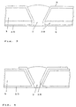
- FIG. 1 shows a section of a section through one that is not part of the invention Sensor chip element, which is in a silicon wafer crystal will be produced.
- t 0.1 mm - 1 mm, preferably 100 ⁇ m - 500 ⁇ m.
- the Containment 2 etched a funnel with the wedge angle of 54.75 ° along the (111) direction.
- the Etching process starts from one surface 3 and sets progresses to the opposite parallel second Surface 4. In the following, the Surface 3 as the front and surface 4 as the back be designated.
- the silicon chip runs parallel to the vertical Walls of the containment.
- two openings 5 and 6 penetrate the front or rear 3 and 4, the diameters of which are related to one another in the manner indicated above.
- the small opening has a diameter between 10 -4 and 10 -1 mm.
- KOH or other known media can be used (cf. A. Heuberger, op. cit., page 125 to 1609).
- All or part of the silicon surface can be etched after the containment z. B. using the known methods of thermal oxidation, the CVD or spin-on-glass technology with a SiO 2 layer 15 which can be silanized for the reason given above. This layer also covers the inner wall of the containment. It is also possible, instead of or additionally, to apply other layers (for example Si 3 N 4 layer) over the SiO 2 layer, likewise by the abovementioned methods.
- other layers for example Si 3 N 4 layer
- the one provided with, usually many containments 2 Wafer is then z. B. on an annular base placed so that the openings of the containments remain free. But it is also possible to polish the wafer on a flat surface Lay plate. With the help of an automatic microdosing device (not shown) the recess 2 filled with a solution forming an ISE membrane. Becomes the lower opening of the Containments left open, so the solution remains due their surface tension and the very small width of the Opening nevertheless in the containment. As is known, it can in such solutions to produce an ion-selective Membrane z. B. PVC, a plasticizer and an ionophore act, dissolved in tetrahydrofuran as a solvent are. Precise recipes for the manufacture of the membrane and Such solutions are the customer information mentioned at the beginning from the company FLUKA. But others can too Membrane materials that are made from the liquid phase leave, as well as other layers (e.g. hydrogel) filled become.
- the opening 5 remains open after filling the solution.
- the wafer provided with the depressions becomes dust-free Atmosphere until the solvent evaporates is and a solidified membrane 7 is formed Has.
- the active membrane surface is which fills the opening 6, very small while the entire membrane volume is very large. It follows thus also a low ionophore depletion over time in the membrane 7.
- FIG. Another embodiment not belonging to the invention is shown in FIG.
- a protective layer 30 z. B. epoxy or Silicon layer
- FIG. 3 shows an exemplary embodiment not belonging to the invention, from which the possibility emerges of the containment geometry in the Area of the small opening on the back of the chip with the help an etch stop layer 18 to be set exactly.
- the etching process automatically on a previously B. heavily doped with boron Etching stop layer interrupted (see: A. Heuberger, a. a. O., Pages 151 and 141 to 1459).
- the small opening of the containment z. B. from the back be opened. Filling and covering the membrane can then be done in the same way as in the previous Examples are given.
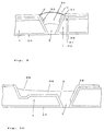
- FIG. 4 shows one possibility of using the containment described above for the production of sensor elements according to the modified coated-film principle.
- the wafer 1 which is provided with an insulating and possibly silanized SiO 2 layer or another insulating layer, is also provided with a thin metal film 16, which is formed in the shape of a funnel or strip in the region of the depression and which, for. B. is applied using known mask technology and vapor deposition or sputtering.
- the metal film which consists for example of silver, a silver layer coated with silver chloride or another electrically conductive layer (e.g. platinum or gold), serves to establish an electrical connection between the membrane 7 introduced later and one on the same silicon chip integrated signal electronics (not shown).
- Chloridation of the vapor-deposited or sputtered Silver layer can e.g. B. according to the known methods by chemical or galvanic means.
- a silicon single crystal wafer is described in the Etched anisotropically (see FIG. 5), with one Indentation 2 shows that when using (100) -oriented Silicon the shape of an inverse truncated pyramid Has. If (110) oriented silicon is used, then so Forms are obtained with a suitable adjustment of the etching masks the recess 2, which is divided by two parallel vertical and two sloping walls. Because of the possible short distance between the parallel vertical containment walls can sensor elements with very low Chip space consumption can be realized. In this 5 shows a section through the sensor element that is parallel to the vertical containment walls runs.
- the containment is produced in a substrate 1 which previously analogous to VMOS-FET (see R. Paul, op. cit., page 336) with a heavily N-doped source layer 22, a P-doped Layer 21 for the channel area and an n-doped Drain layer 23 is provided.
- the drain area can, as shown in Figure 5, through the silicon substrate 1 itself. But it is also possible, analogous to VMOS-FET to use an additional layer that is epitaxial can be generated on the substrate. Subsequently becomes a solution forming the ISE membrane in the recess 2 filled and until the solvent evaporates and formation of the membrane 7 left.
- the channel area is located in the area of the larger opening 5.
- a layer structure such that the channel area 21 is located in the area of the smaller opening 6.
- the gate dielectric consists, as in the known ISFET z. B. from SiO 2 or a SiO 2 / Si 3 N 4 layer sequence.
- the large opening of the containment can be after the ion selective Membrane is formed, as shown in Fig. 2, be covered with a protective layer.
- the membrane 7 forms the so-called "gate” of the VIS-FET. It is expressly noted that in addition to the present one “Depletion type” also the so-called “enrichment type” as well as ISFET with reversed line types (n and p interchanged) can be provided.
- FIGS. 5 and 6 are also suitable for the production of VISFET with a solid-state membrane and an additional electrochemically relevant layer 7 which replaces the liquid membrane.
- the dielectric layer 15 can thus be formed on the silicon as a result of an SiO 2 layer and an additional solid layer (eg Si 3 N 4 , Ta 2 O 5 or the like).
- This additional layer can, for. B. on the SiO 2 using the known CVD, sputtering or sol-gel technology and serves as an ion-selective solid membrane.
- This layer can be made of hydrogel, for example exist that the electrochemical response of the underlying Solid-state membrane extremely delayed, so that by combining the VISFET structures with and without a hydrogel layer 7 the known possibility for differential measurement results.
- the ion-selective sensor elements shown above with Micromechanically structured containment can also do so be modified so that they have a solidified inner electrolyte layer work according to the half-cell principle.
- Figures 7 and 8 show two embodiments.
- the example 7 differs from FIG. 4 only in that that the lead electrode 16 is not so deep in the containment reaches in and over the ion-selective liquid membrane 7, a solidified inner electrolyte layer 31 is arranged is.
- the lead electrode can e.g. B. from one with Silver chloride coated silver film exist.
- the ion-selective liquid membrane e.g. PVC membrane
- the internal electrolyte is poured in a further casting process.
- the inner electrolyte can be made in a known manner Saline solution (z. B. KCl) exist, the z. B. with gelatin, agar or polyvinyl alcohol is added, so that some Time after filling the initially liquid internal electrolyte a solidified inner electrolyte layer in the containment above the ion-selective liquid membrane.
- a further variant is shown in FIG differs from the previous one in that the large containment 2 is a small containment 32, that is directly connected to the big one and also itself by the anisotropic etching method described above can generate.
- This structure facilitates the separation from Liquid membrane and inner electrolyte layer.
- VISFET structures with an internal electrolyte can also be used produce ( Figure 9).
- This embodiment differs from the example according to FIG. 5 in that that over the dielectric layer 15 z.
- B. a silver layer 33 evaporated or sputtered and lithographically is structured with a layer of silver chloride is covered.
- the containment becomes analogous, for example from Figure 8 with liquid membrane 7 and internal electrolyte 31 provided.
- capillary channels can be V-shaped or Have U-shaped cross sections.
- FIG. 10 shows a structure according to FIG. 4 as an example on average with a capillary channel 34 and a Filling opening 35 is provided.
- the membrane fluid will filled into the large filling opening. It is due to the Capillary forces in the channel promoted and then fills that Containment. It is also possible from a filling opening from several containments on surrounding chips or on to fill all chips of a wafer with membrane liquid. The filler opening can then be separated Chips of a wafer are separated. To improve the Flow behavior of the membrane solution can be filled under Solvent atmosphere take place.
- FIG. 11 shows a system of capillary channels 34 and large filling openings 35 shown.
- a chip 39 At the end of each Capillary channel is a chip 39 and the containment 2 of a sensor element.
- FIG. 12 shows a silicon chip with an ion-selective one Membrane 7 in a containment containing its active membrane surface on which the back of the chip has 4.
- On the front of the chip 3 are the contact surfaces of the chip, that with the help of fine bond wires 36 with the housing contacts get connected.
- a carrier 38 and the whole Sensor chip sealed on the front with plastic become.
Description
- modifiziertes coated-film-Prinzip
- modifiziertes Halbzellen-Prinzip
- modifiziertes ISFET-Prinzip.
- Versehen der Vorderseite eines Siliziumsubstrates mit vertikal übereinander angeordneten n- und p-leitenden Schichten für Source, Drain sowie Gätebereich, -
- Ätzen eines Containments in einem dünnen Siliziumsubstrat, bei dem das Containment von einer Öffnung gebildet wird, die sich von einer ersten Oberfläche zu einer gegenüberliegenden parallelen zweiten Oberfläche - sich verjüngend - erstreckt, so daß deren Oberflächen verbunden sind, und daß diese Folgen von Schichten an der Containment-Innenwandung ansteht;
- Versehen der Containment-Innenwandung mit einer dielektrischen Schicht;
- Befüllen des Containments mit einer Membran-Lösung über die große Öffnung, welche Membranlösung nach der Verdampfung des Lösungsmittels eine verfestigte, ionenselektive, mit der dielektrischen Schicht in Kontakt stehende Membran (7) bildet.
- Fig. 1
- Ausschnitt aus einem Sensor-Chip mit ionenselektiver Membran in mikrostrukturiertem Containment,
- Fig. 2
- einen Ausschnitt mit abgedeckter Membran,
- Fig. 3
- einen Ausschnitt mit einem Containment, das mit Hilfe einer Ätzstoppschicht hergestellt wurde,
- Fig. 4
- ein ionenselektives Sensorelement nach dem "coa-ted-film-Prinzip",
- Fig. 5
- einen vertikalen ISFET (VISFET),
- Fig. 6
- eine weitere VISFET-Variante,
- Fig. 7 und Fig. 8
- zwei Ausführungsformen von ionenselektiven Sensorelementen nach dem HalbzellenPrinzip,
- Fig. 9
- einen VISFET mit Innenelektrolyt,
- Fig. 10
- ein Sensorelement mit Kapillarkanal und Einfüllöffnung,
- Fig. 11
- eine kapillare Kanalstruktur zur Füllung der Containments mit Membranflüssigkeit,
- Fig. 12
- einen Sensor-Chip in einem Gehäuse.
Claims (16)
- Verfahren zur Herstellung von Trägern mit miniaturisierten Chemo- und Biosensorelementen, mit folgenden Verfahrensschritten:Ätzen eines Containments (2) in einem dünnen Siliziumsubstrat (1), bei dem das Containment (2) von einer (Öffnung (5,6) gebildet ist, die sich von einer ersten Oberfläche (3) zu einer gegenüberliegenden parallelen zweiten Oberfläche (4) - sich verjüngend - erstreckt, so daß deren Oberflächen (Vorderseite 3, Rückseite 4) verbunden sind,Einbringen wenigstens einer Elektrode (16) in das Containment (2), die an seiner Innenwandung anliegt,Befüllen des Containments (2) mit einer Membranlösung über die große Öffnung, welche Membranlösung nach Verdampfung des Lösungsmittels eine verfestigte ionenselektive, mit der Elektrode (16) im Kontakt stehende Membran (7) bildet.
- Verfahren nach Anspruch 1, dadurch gekennzeichnet, daß ein anisotropes Ätzen des Containments (2) in einem (100)- oder (110)-orientierten Siliziumsubstrat (1) erfolgt, so daß eine Öffnung (5,6) gebildet wird, die sich von einer ersten Oberfläche (Vorderseite 3) zu einer gegenüberliegenden parallelen zweiten Oberfläche (Rückseite 4) verjüngt, wobei das im (100)-orientierten Siliziumsubstrat (1) erzeugte Containment (2) pyramidenstumpfförmig ist und entsprechend das im (110)-orientierten Siliziumsubstrat erzeugte Containment zwei parallele senkrechte und zwei geneigte Wände aufweist.
- Verfahren nach Anspruch 1 oder 2, dadurch gekennzeichnet, daß das Siliziumsubstrat (1) vor dem Ätzen mit seiner Ätzstop-Schicht (18) auf der Rückseite (4) versehen wird, daß anschließend das Substrat (1) von der Vorderseite (3) bis zur Ätzstop-Schicht (18) geätzt wird, und daß anschließend die Ätzstop-Schicht (18) im Bereich der Öffnungsverengung bis zur Rückseite (4) durchgeätzt wird.
- Verfahren nach Anspruch 1 bis 3, dadurch gekennzeichnet, daß die Vorder- (3) und Rückseite (4) mit Hilfe einer thermischen Oxidation oder mit CVD- oder mit Sol-Gel-Technik wenigstens im Bereich der Öffnungen (5, 6) des Containments (2) sowie die Innenflächen des Containments mit einer durchgehend SiO2-Schicht versehen werden.
- Verfahren nach wenigstens einem der vorhergehenden Ansprüche, dadurch gekennzeichnet, daß die SiO2-Schicht, die die Phasengrenze zur ionenselektiven Membran bildet, an der Oberfläche silanisiert wird.
- Verfahren nach wenigstens einem der vorhergehenden Ansprüche, dadurch gekennzeichnet, daß anstelle oder zusätzlich zur SiO2-Schicht eine weitere Schicht (z. B. Si3N4) auf die Innenwandung des Containments (2) aufgebracht wird.
- Verfahren nach wenigstens einem der vorhergehenden Ansprüche, dadurch gekennzeichnet, daß die Elektrode (16) aus einem aufgedampften oder aufgesputterten und lithographisch strukturiertem Silberfilm, einem mit Silberchlorid überzogenen Silberfilm oder einem anderen leitenden Film besteht.
- Verfahren nach wenigstens einem der Ansprüche 1 bis 7, dadurch gekennzeichnet, daß in das Containment (2) eine Lösung eingefüllt wird, die nach Verfestigung eine Elektrolytschicht, beispielsweise eine Hydrogelschicht, ausbildet, wobei die Elektrode (16) über diese Elektrolytschicht mit der Membran in Kontakt steht.
- Verfahren nach wenigstens einem der vorhergehenden Ansprüche, dadurch gekennzeichnet, daß anstelle der ionenselektiven Membran in das Containment (2) eine Membranlösung eingefüllt wird, die nach Verfestigung eine Membran (7) ausbildet, in der ein biochemisch aktives Material eingelagert ist.
- Verfahren zur Herstellung eines vertikalen ISFET (VIS-FET) mit folgenden Verfahrensschritten:Versehen der Vorderseite eines Siliziumsubstrates (1) mit vertikal übereinander angeordneten n- und p-leitenden Schichten für Source, Drain sowie Gatebereich,Ätzen eines Containments (2) in einem dünnen Siliziumsubstrat, bei dem das Containment (2) von einer Öffnung (5,6) gebildet wird, die sich von einer ersten Oberfläche (3) zu einer gegenüberliegenden parallelen zweiten Oberfläche (4) - sich verjüngend - erstreckt, so daß deren Oberflächen (3,4) verbunden sind, und daß diese Folgen von Schichten an der Containment-Innenwandung ansteht;Versehen der Containment-Innenwandung mit einer dielektrischen Schicht;Befüllen des Containments mit einer Membran-Lösung über die große Öffnung, welche Membranlösung nach der Verdampfung des Lösungsmittels eine verfestigte, ionenselektive, mit der dielektrischen Schicht in Kontakt stehende Membran (7) bildet.
- Verfahren nach Anspruch 10, dadurch gekennzeichnet, daß über der ionenselektiven Membran (7) eine verfestigte Innenelektrolytschicht (31) im Containment (2) aufgebracht wird, die mit einem Gatekontakt (33) des vertikalen ISFET, z. B. aus einer mit Silberchlorid überzogenen Silberschicht, in Kontakt gebracht wird.
- Verfahren nach Anspruch 11, dadurch gekennzeichnet, daß das Containment von der Substratrückseite (4) aus geätzt wird und die kleine Containmentöffnung mit der aktiven Membranoberfläche an der Substratvorderseite angeordnet wird.
- Verfahren nach wenigstens einem der vorhergehenden Ansprüche, dadurch gekennzeichnet, daß das Containment (2) an einen kapillaren Kanal (34) mit einer Einfüllöffnung (35) verbunden wird, in die die Membranlösung unter Lösungsmittel-Atmosphäre eingefüllt wird.
- Verfahren nach Anspruch 13, dadurch gekennzeichnet, daß von einer Einfüllöffnung aus mehrere Containments auf weiteren, umliegenden Chips (39), bzw. auf allen Chips eines Siliziumsubstrats mit Membranflüssigkeit gefüllt und die Chips anschließend vereinzelt werden.
- Verfahren nach wenigstens einem der vorhergehenden Ansprüche, dadurch gekennzeichnet, daß die große Öffnung (5) des Containments und/oder die Einfüllöffnung sowie der kapillare Kanal (34) mit einer Schutzschicht (30) abgedeckt werden.
- Verfahren nach wenigstens einem der vorhergehenden Ansprüche, dadurch gekennzeichnet, daß das Sensorelement in ein Gehäuse eingebaut oder mit einer Schutzschicht versiegelt wird und daß seine aktiven Membranoberflächen an der Rückseite (4) mit einer Meßflüssigkeit in Kontakt stehen.
Applications Claiming Priority (3)
| Application Number | Priority Date | Filing Date | Title |
|---|---|---|---|
| DE4115414 | 1991-05-10 | ||
| DE4115414A DE4115414C2 (de) | 1991-05-10 | 1991-05-10 | Verfahren zur Herstellung von miniaturisierten Chemo- und Biosensorelementen mit ionenselektiver Membran sowie von Trägern für diese Elemente |
| PCT/EP1992/000990 WO1992021020A1 (de) | 1991-05-10 | 1992-05-06 | Verfahren zur herstellung von miniaturisierten chemo- und biosensorelementen mit ionenselektiver membran sowie von trägern für diese elemente |
Publications (2)
| Publication Number | Publication Date |
|---|---|
| EP0538428A1 EP0538428A1 (de) | 1993-04-28 |
| EP0538428B1 true EP0538428B1 (de) | 2002-09-11 |
Family
ID=6431468
Family Applications (1)
| Application Number | Title | Priority Date | Filing Date |
|---|---|---|---|
| EP92909188A Expired - Lifetime EP0538428B1 (de) | 1991-05-10 | 1992-05-06 | Verfahren zur herstellung von miniaturisierten chemo- und biosensorelementen mit ionenselektiver membran sowie von trägern für diese elemente |
Country Status (8)
| Country | Link |
|---|---|
| US (1) | US5393401A (de) |
| EP (1) | EP0538428B1 (de) |
| JP (1) | JP3111283B2 (de) |
| AT (1) | ATE224054T1 (de) |
| DE (2) | DE4115414C2 (de) |
| DK (1) | DK0538428T3 (de) |
| ES (1) | ES2182820T3 (de) |
| WO (1) | WO1992021020A1 (de) |
Families Citing this family (76)
| Publication number | Priority date | Publication date | Assignee | Title |
|---|---|---|---|---|
| GB8927377D0 (en) * | 1989-12-04 | 1990-01-31 | Univ Edinburgh | Improvements in and relating to amperometric assays |
| US6375899B1 (en) | 1993-11-01 | 2002-04-23 | Nanogen, Inc. | Electrophoretic buss for transport of charged materials in a multi-chamber system |
| US6287517B1 (en) | 1993-11-01 | 2001-09-11 | Nanogen, Inc. | Laminated assembly for active bioelectronic devices |
| US6225059B1 (en) | 1993-11-01 | 2001-05-01 | Nanogen, Inc. | Advanced active electronic devices including collection electrodes for molecular biological analysis and diagnostics |
| US6638482B1 (en) | 1993-11-01 | 2003-10-28 | Nanogen, Inc. | Reconfigurable detection and analysis apparatus and method |
| US6331274B1 (en) | 1993-11-01 | 2001-12-18 | Nanogen, Inc. | Advanced active circuits and devices for molecular biological analysis and diagnostics |
| US6319472B1 (en) | 1993-11-01 | 2001-11-20 | Nanogen, Inc. | System including functionally separated regions in electrophoretic system |
| US20040077074A1 (en) * | 1993-11-01 | 2004-04-22 | Nanogen, Inc. | Multi-chambered analysis device |
| DE4337418C2 (de) * | 1993-11-03 | 1997-09-18 | Inst Chemo Biosensorik | Verfahren zur Herstellung eines Biosensorelementes in Silizium-Technologie in einem Full-Wafer-Prozeß |
| DE4408352C2 (de) * | 1994-03-12 | 1996-02-08 | Meinhard Prof Dr Knoll | Miniaturisierter stofferkennender Durchflußsensor sowie Verfahren zu seiner Herstellung |
| DE4410224C2 (de) * | 1994-03-24 | 1996-02-29 | Meinhard Prof Dr Knoll | Miniaturisiertes Durchfluß-Analysesystem |
| US6403367B1 (en) * | 1994-07-07 | 2002-06-11 | Nanogen, Inc. | Integrated portable biological detection system |
| US7857957B2 (en) * | 1994-07-07 | 2010-12-28 | Gamida For Life B.V. | Integrated portable biological detection system |
| DE4426507C2 (de) * | 1994-07-27 | 2001-04-26 | Inst Chemo Biosensorik | Sensoren auf der Basis von Mikrostrukturen |
| DE4427921C2 (de) * | 1994-08-06 | 2002-09-26 | Forschungszentrum Juelich Gmbh | Chemische Sensoren, insbesondere Biosensoren, auf Siliciumbasis |
| DE4429739C1 (de) * | 1994-08-22 | 1996-03-28 | Inst Chemo Biosensorik | Verfahren zum Befüllen eines Containments |
| DE9417289U1 (de) * | 1994-10-27 | 1995-01-26 | Meinke Peter Prof Dr Ing | Detektoreinrichtung, Detektorsystem und Immunosensor zum Erkennen von Bränden |
| US5554273A (en) * | 1995-07-26 | 1996-09-10 | Praxair Technology, Inc. | Neural network compensation for sensors |
| DE19546535C2 (de) * | 1995-12-13 | 2000-02-03 | Karl Cammann | Meßkartusche für flüssige oder gasförmige Proben, Verfahren zu deren Betreiben und deren Verwendung |
| DE19602861C2 (de) * | 1996-01-28 | 1997-12-11 | Meinhard Prof Dr Knoll | Probenahmesystem für in Trägerflüssigkeiten enthaltene Analyte sowie Verfahren zu seiner Herstellung |
| US6355198B1 (en) | 1996-03-15 | 2002-03-12 | President And Fellows Of Harvard College | Method of forming articles including waveguides via capillary micromolding and microtransfer molding |
| DE19628052C1 (de) * | 1996-07-11 | 1997-11-27 | Fraunhofer Ges Forschung | Sensor- und/oder Trennelement sowie Verfahren zu dessen Herstellung und Anwendung desselben |
| US6811037B2 (en) | 1996-07-11 | 2004-11-02 | Fraunhofer-Fesellschaft Zur Forderung Derangewandten Forschung E.V. | Sensor and/or separating element and process for the production and use thereof |
| DE19641777C2 (de) * | 1996-10-10 | 2001-09-27 | Micronas Gmbh | Verfahren zum Herstellen eines Sensors mit einer Metallelektrode in einer MOS-Anordnung |
| DE19725050C2 (de) * | 1997-06-13 | 1999-06-24 | Fraunhofer Ges Forschung | Anordnung zur Detektion biochemischer oder chemischer Substanzen mittels Fluoreszenzlichtanregung und Verfahren zu deren Herstellung |
| WO1999019067A1 (en) * | 1997-10-10 | 1999-04-22 | Biosepra, Inc. | Aligned multiwell multiplate stack and method for processing biological/chemical samples using the same |
| US20020144905A1 (en) * | 1997-12-17 | 2002-10-10 | Christian Schmidt | Sample positioning and analysis system |
| CA2316966C (en) * | 1997-12-17 | 2008-04-08 | Horst Vogel | Positioning and electrophysiological characterization of individual cells and reconstituted membrane systems on microstructured carriers |
| US7244349B2 (en) | 1997-12-17 | 2007-07-17 | Molecular Devices Corporation | Multiaperture sample positioning and analysis system |
| DE19757706C2 (de) * | 1997-12-23 | 2002-01-24 | Jandratek Gmbh | Substrat, Vorrichtung und Verfahren zur schnellen Auswertung von Bindungsreaktionen durch interferometrische Schichtdickenmessung |
| GB9810568D0 (en) * | 1998-05-18 | 1998-07-15 | Imco 1097 Limited | Electrode system |
| US6041643A (en) * | 1998-07-27 | 2000-03-28 | General Electric Company | Gas sensor with protective gate, method of forming the sensor, and method of sensing |
| US6182500B1 (en) | 1998-07-27 | 2001-02-06 | General Electric Company | Gas sensor with protective gate, method of forming the sensor, and method of sensing |
| DE19848112C2 (de) * | 1998-10-19 | 2001-12-13 | Meinhard Knoll | Minimalinvasives Sensorsystem |
| US7115422B1 (en) * | 1998-10-23 | 2006-10-03 | Micron Technology, Inc. | Separation apparatus including porous silicon column |
| US6762057B1 (en) * | 1998-10-23 | 2004-07-13 | Micron Technology, Inc. | Separation apparatus including porous silicon column |
| US6387724B1 (en) | 1999-02-26 | 2002-05-14 | Dynamics Research Corporation | Method of fabricating silicon-on-insulator sensor having silicon oxide sensing surface |
| DE19929264A1 (de) * | 1999-06-25 | 2001-01-11 | Meinhard Knoll | Universaltransducer |
| CA2385482C (en) * | 1999-10-01 | 2011-01-18 | Jon Wulff Petersen | A substrate and a method for determining and/or monitoring electrophysiological properties of ion channels |
| US6682649B1 (en) * | 1999-10-01 | 2004-01-27 | Sophion Bioscience A/S | Substrate and a method for determining and/or monitoring electrophysiological properties of ion channels |
| US6645359B1 (en) | 2000-10-06 | 2003-11-11 | Roche Diagnostics Corporation | Biosensor |
| DE10003507B4 (de) * | 2000-01-27 | 2004-06-03 | Knoll, Meinhard, Prof. Dr. | Vorrichtung und Verfahren zur Entnahme von Flüssigkeiten aus körpereigenem Gewebe und Bestimmung von Stoffkonzentrationen in dieser Flüssigkeit |
| US6551496B1 (en) | 2000-03-03 | 2003-04-22 | Ysi Incorporated | Microstructured bilateral sensor |
| US6770322B1 (en) | 2000-03-03 | 2004-08-03 | Ysi Incorporated | Method of making a platform for use in a sensor in a microfluidic device |
| DE10010587A1 (de) | 2000-03-03 | 2001-09-06 | Roche Diagnostics Gmbh | System zur Bestimmung von Analytkonzentrationen in Körperflüssigkeiten |
| DE10023015A1 (de) * | 2000-05-05 | 2002-01-24 | Inst Chemo Biosensorik | Verdahren zur Herstellung eines dreidimensionalen Sensorelementes |
| US7270730B2 (en) | 2000-08-04 | 2007-09-18 | Essen Instruments, Inc. | High-throughput electrophysiological measurement system |
| US7067046B2 (en) * | 2000-08-04 | 2006-06-27 | Essen Instruments, Inc. | System for rapid chemical activation in high-throughput electrophysiological measurements |
| US6764652B2 (en) * | 2001-01-24 | 2004-07-20 | The Regents Of The University Of Michigan | Micromachined device for receiving and retaining at least one liquid droplet, method of making the device and method of using the device |
| DE10123803C1 (de) * | 2001-05-16 | 2002-10-31 | Roche Diagnostics Gmbh | Elektrochemische Messzelle |
| DE10155930B4 (de) * | 2001-11-14 | 2020-09-24 | Nano Analytik Gmbh | Feldeffekttransistor-Sensor |
| US10022078B2 (en) | 2004-07-13 | 2018-07-17 | Dexcom, Inc. | Analyte sensor |
| US7407570B2 (en) * | 2002-03-13 | 2008-08-05 | The Charles Stark Draper Laboratory, Inc. | Disposable, self-administered electrolyte test |
| US7101472B2 (en) * | 2002-03-13 | 2006-09-05 | The Charles Stark Draper Laboratory, Inc. | Microfluidic ion-selective electrode sensor system |
| US7022287B2 (en) * | 2002-05-08 | 2006-04-04 | Sandia National Laboratories | Single particle electrochemical sensors and methods of utilization |
| DE10260961A1 (de) * | 2002-12-20 | 2004-07-01 | Endress + Hauser Conducta Gesellschaft für Mess- und Regeltechnik mbH + Co. KG | Halbleitersensor mit frontseitiger Kontaktierung |
| GB0306163D0 (en) * | 2003-03-18 | 2003-04-23 | Univ Cambridge Tech | Embossing microfluidic sensors |
| JP4438049B2 (ja) * | 2003-08-11 | 2010-03-24 | キヤノン株式会社 | 電界効果トランジスタ及びそれを用いたセンサ並びにその製造方法 |
| US7920906B2 (en) | 2005-03-10 | 2011-04-05 | Dexcom, Inc. | System and methods for processing analyte sensor data for sensor calibration |
| US7138672B2 (en) * | 2003-09-25 | 2006-11-21 | Agilent Technologies, Inc. | Apparatus and method for making a tensile diaphragm with an insert |
| US9247900B2 (en) | 2004-07-13 | 2016-02-02 | Dexcom, Inc. | Analyte sensor |
| JP4547956B2 (ja) * | 2004-03-24 | 2010-09-22 | ヤマハ株式会社 | 半導体装置、及び、チップサイズパッケージ |
| US20060020192A1 (en) | 2004-07-13 | 2006-01-26 | Dexcom, Inc. | Transcutaneous analyte sensor |
| CA2635670C (en) | 2005-12-27 | 2011-07-12 | Bayer Healthcare Llc | Electrochemical sensor system using a substrate with at least one aperture and method of making the same |
| WO2009045091A2 (en) * | 2007-10-05 | 2009-04-09 | Mimos Berhad | A vertical thin polysilicon substrate isfet |
| US11730407B2 (en) | 2008-03-28 | 2023-08-22 | Dexcom, Inc. | Polymer membranes for continuous analyte sensors |
| US8682408B2 (en) | 2008-03-28 | 2014-03-25 | Dexcom, Inc. | Polymer membranes for continuous analyte sensors |
| US8583204B2 (en) | 2008-03-28 | 2013-11-12 | Dexcom, Inc. | Polymer membranes for continuous analyte sensors |
| US20100252429A1 (en) * | 2009-04-07 | 2010-10-07 | Rao K Jagan | Ion-selective electrode |
| NL2003340C2 (en) * | 2009-08-10 | 2011-02-14 | Univ Delft Tech | Method of manufacturing a micro unit and micro unit for use in a microscope. |
| WO2012091540A1 (en) * | 2010-12-29 | 2012-07-05 | Mimos Berhad | Integrated microfluidics sensor |
| JP5389892B2 (ja) * | 2011-11-15 | 2014-01-15 | 株式会社東芝 | イオン選択性電極、イオン選択性電極モジュール、及びイオン選択性電極の製造方法 |
| US20140174923A1 (en) * | 2012-12-26 | 2014-06-26 | K. Jagan M. Rao | Ion selective electrode |
| US8896032B2 (en) * | 2013-01-23 | 2014-11-25 | International Business Machines Corporation | Self-aligned biosensors with enhanced sensitivity |
| JP6783704B2 (ja) * | 2017-05-31 | 2020-11-11 | 株式会社日立ハイテク | 陰イオン選択性電極及びその製造方法 |
| US20220365019A1 (en) * | 2021-05-14 | 2022-11-17 | Taiwan Semiconductor Manufacturing Company Ltd. | Fluid sensor system |
Family Cites Families (7)
| Publication number | Priority date | Publication date | Assignee | Title |
|---|---|---|---|---|
| US4645562A (en) * | 1985-04-29 | 1987-02-24 | Hughes Aircraft Company | Double layer photoresist technique for side-wall profile control in plasma etching processes |
| US4592824A (en) * | 1985-09-13 | 1986-06-03 | Centre Suisse D'electronique Et De Microtechnique S.A. | Miniature liquid junction reference electrode and an integrated solid state electrochemical sensor including the same |
| US4874500A (en) * | 1987-07-15 | 1989-10-17 | Sri International | Microelectrochemical sensor and sensor array |
| US5111221A (en) * | 1988-05-13 | 1992-05-05 | United States Of America As Represented By The Secretary Of The Navy | Receptor-based sensor |
| US4874499A (en) * | 1988-05-23 | 1989-10-17 | Massachusetts Institute Of Technology | Electrochemical microsensors and method of making such sensors |
| JP3001104B2 (ja) * | 1989-10-04 | 2000-01-24 | オリンパス光学工業株式会社 | センサー構造体及びその製造法 |
| US5183549A (en) * | 1990-01-26 | 1993-02-02 | Commtech International Management Corporation | Multi-analyte sensing electrolytic cell |
-
1991
- 1991-05-10 DE DE4115414A patent/DE4115414C2/de not_active Expired - Fee Related
-
1992
- 1992-05-06 DK DK92909188T patent/DK0538428T3/da active
- 1992-05-06 JP JP04508550A patent/JP3111283B2/ja not_active Expired - Fee Related
- 1992-05-06 US US07/966,148 patent/US5393401A/en not_active Expired - Fee Related
- 1992-05-06 DE DE59209966T patent/DE59209966D1/de not_active Expired - Fee Related
- 1992-05-06 ES ES92909188T patent/ES2182820T3/es not_active Expired - Lifetime
- 1992-05-06 AT AT92909188T patent/ATE224054T1/de not_active IP Right Cessation
- 1992-05-06 WO PCT/EP1992/000990 patent/WO1992021020A1/de active IP Right Grant
- 1992-05-06 EP EP92909188A patent/EP0538428B1/de not_active Expired - Lifetime
Non-Patent Citations (1)
| Title |
|---|
| SZE S.M.: "Physics of Semiconductor Devices", 1981, JOHN WILEY & SONS, SINGAPORE * |
Also Published As
| Publication number | Publication date |
|---|---|
| ATE224054T1 (de) | 2002-09-15 |
| DE59209966D1 (de) | 2002-10-17 |
| DE4115414A1 (de) | 1992-11-12 |
| WO1992021020A1 (de) | 1992-11-26 |
| ES2182820T3 (es) | 2003-03-16 |
| US5393401A (en) | 1995-02-28 |
| JP3111283B2 (ja) | 2000-11-20 |
| JPH06500178A (ja) | 1994-01-06 |
| DE4115414C2 (de) | 1995-07-06 |
| EP0538428A1 (de) | 1993-04-28 |
| DK0538428T3 (da) | 2003-01-20 |
Similar Documents
| Publication | Publication Date | Title |
|---|---|---|
| EP0538428B1 (de) | Verfahren zur herstellung von miniaturisierten chemo- und biosensorelementen mit ionenselektiver membran sowie von trägern für diese elemente | |
| EP0750744B1 (de) | Miniaturisierte durchflussmesskammer mit integrierten chemo- und/oder biosensorelementen | |
| EP1062501B1 (de) | Referenzelektrode | |
| DE3535904C2 (de) | Kapazitiver Absolutdruck-Sensor | |
| DE102014100743B4 (de) | Chipgehäuse und Verfahren zu seiner Herstellung | |
| DE4031425A1 (de) | Fet-sensorvorrichtung vom flusszellenadaptiv-typ und herstellungsverfahren | |
| DE19621996A1 (de) | Verfahren zur Herstellung einer Kombination eines Drucksensors und eines elektrochemischen Sensors | |
| WO2009077234A2 (de) | Verfahren zum herstellen eines kappenwafers für einen sensor | |
| EP0064970A2 (de) | Medizinische Sonde | |
| DE10213805A1 (de) | Gassensor und Verfahren zum Herstellen eines Gassensors | |
| DE3507820A1 (de) | Kapazitiver wandler | |
| DE4309206C1 (de) | Halbleitervorrichtung mit einem Kraft- und/oder Beschleunigungssensor | |
| DE10332725A1 (de) | Verfahren zur selbstjustierenden Verkleinerung von Strukturen | |
| EP0873789A2 (de) | Vorrichtung zur gekapselten Aufnahme eines Materials | |
| EP0382831A1 (de) | Chemosensitiver wandler. | |
| WO2000036385A1 (de) | Verfahren zum erzeugen einer mikromechanischen struktur für ein mikro-elektromechanisches element | |
| DE10049901A1 (de) | Vorrichtung und Verfahren zur elektrisch beschleunigten Immobilisierung und zur Detektion von Molekülen | |
| DE2736200A1 (de) | Chemisch sensitiver feldeffekt- transistor und verfahren zur herstellung desselben | |
| DE4131927C2 (de) | Verfahren zur Herstellung eines Sensorelementes mit wenigstens einer ionenselektiven Elektrode in einem integrierten Schaltkreis | |
| DE19929264A1 (de) | Universaltransducer | |
| DE10019408C2 (de) | Feldeffekttransistor, insbesondere zur Verwendung als Sensorelement oder Beschleunigungssensor, und Verfahren zu dessen Herstellung | |
| EP0645621A2 (de) | Sensoranordnung | |
| DE4426507A1 (de) | Sensoren auf der Basis von Mikrostrukturen | |
| DE19636461A1 (de) | Sensoranordnung und Verfahren zu deren Herstellung | |
| DE4337418A1 (de) | Biosensorelement in Siliziumtechnologie und Verfahren zu seiner Herstellung |
Legal Events
| Date | Code | Title | Description |
|---|---|---|---|
| PUAI | Public reference made under article 153(3) epc to a published international application that has entered the european phase |
Free format text: ORIGINAL CODE: 0009012 |
|
| AK | Designated contracting states |
Kind code of ref document: A1 Designated state(s): AT BE CH DE DK ES FR GB GR IT LI LU MC NL SE |
|
| 17P | Request for examination filed |
Effective date: 19930505 |
|
| 17Q | First examination report despatched |
Effective date: 19970213 |
|
| GRAG | Despatch of communication of intention to grant |
Free format text: ORIGINAL CODE: EPIDOS AGRA |
|
| GRAG | Despatch of communication of intention to grant |
Free format text: ORIGINAL CODE: EPIDOS AGRA |
|
| GRAH | Despatch of communication of intention to grant a patent |
Free format text: ORIGINAL CODE: EPIDOS IGRA |
|
| GRAH | Despatch of communication of intention to grant a patent |
Free format text: ORIGINAL CODE: EPIDOS IGRA |
|
| GRAA | (expected) grant |
Free format text: ORIGINAL CODE: 0009210 |
|
| AK | Designated contracting states |
Kind code of ref document: B1 Designated state(s): AT BE CH DE DK ES FR GB GR IT LI LU MC NL SE |
|
| REF | Corresponds to: |
Ref document number: 224054 Country of ref document: AT Date of ref document: 20020915 Kind code of ref document: T |
|
| REG | Reference to a national code |
Ref country code: GB Ref legal event code: FG4D Free format text: NOT ENGLISH |
|
| REG | Reference to a national code |
Ref country code: CH Ref legal event code: EP |
|
| REF | Corresponds to: |
Ref document number: 59209966 Country of ref document: DE Date of ref document: 20021017 |
|
| GBT | Gb: translation of ep patent filed (gb section 77(6)(a)/1977) |
Effective date: 20021014 |
|
| REG | Reference to a national code |
Ref country code: CH Ref legal event code: NV Representative=s name: PATMED AG |
|
| REG | Reference to a national code |
Ref country code: DK Ref legal event code: T3 |
|
| REG | Reference to a national code |
Ref country code: GR Ref legal event code: EP Ref document number: 20020404188 Country of ref document: GR |
|
| REG | Reference to a national code |
Ref country code: ES Ref legal event code: FG2A Ref document number: 2182820 Country of ref document: ES Kind code of ref document: T3 |
|
| ET | Fr: translation filed | ||
| PLBE | No opposition filed within time limit |
Free format text: ORIGINAL CODE: 0009261 |
|
| STAA | Information on the status of an ep patent application or granted ep patent |
Free format text: STATUS: NO OPPOSITION FILED WITHIN TIME LIMIT |
|
| 26N | No opposition filed |
Effective date: 20030612 |
|
| PGFP | Annual fee paid to national office [announced via postgrant information from national office to epo] |
Ref country code: GB Payment date: 20050425 Year of fee payment: 14 |
|
| PGFP | Annual fee paid to national office [announced via postgrant information from national office to epo] |
Ref country code: MC Payment date: 20050511 Year of fee payment: 14 |
|
| PGFP | Annual fee paid to national office [announced via postgrant information from national office to epo] |
Ref country code: FR Payment date: 20050512 Year of fee payment: 14 Ref country code: SE Payment date: 20050512 Year of fee payment: 14 Ref country code: NL Payment date: 20050512 Year of fee payment: 14 Ref country code: CH Payment date: 20050512 Year of fee payment: 14 |
|
| PGFP | Annual fee paid to national office [announced via postgrant information from national office to epo] |
Ref country code: ES Payment date: 20050513 Year of fee payment: 14 Ref country code: DK Payment date: 20050513 Year of fee payment: 14 |
|
| PGFP | Annual fee paid to national office [announced via postgrant information from national office to epo] |
Ref country code: LU Payment date: 20050519 Year of fee payment: 14 |
|
| PGFP | Annual fee paid to national office [announced via postgrant information from national office to epo] |
Ref country code: DE Payment date: 20050520 Year of fee payment: 14 Ref country code: AT Payment date: 20050520 Year of fee payment: 14 |
|
| PGFP | Annual fee paid to national office [announced via postgrant information from national office to epo] |
Ref country code: GR Payment date: 20050524 Year of fee payment: 14 |
|
| PGFP | Annual fee paid to national office [announced via postgrant information from national office to epo] |
Ref country code: BE Payment date: 20050606 Year of fee payment: 14 |
|
| PG25 | Lapsed in a contracting state [announced via postgrant information from national office to epo] |
Ref country code: GB Free format text: LAPSE BECAUSE OF NON-PAYMENT OF DUE FEES Effective date: 20060506 Ref country code: AT Free format text: LAPSE BECAUSE OF NON-PAYMENT OF DUE FEES Effective date: 20060506 |
|
| PG25 | Lapsed in a contracting state [announced via postgrant information from national office to epo] |
Ref country code: SE Free format text: LAPSE BECAUSE OF NON-PAYMENT OF DUE FEES Effective date: 20060507 |
|
| PG25 | Lapsed in a contracting state [announced via postgrant information from national office to epo] |
Ref country code: ES Free format text: LAPSE BECAUSE OF NON-PAYMENT OF DUE FEES Effective date: 20060508 |
|
| PG25 | Lapsed in a contracting state [announced via postgrant information from national office to epo] |
Ref country code: MC Free format text: LAPSE BECAUSE OF NON-PAYMENT OF DUE FEES Effective date: 20060531 Ref country code: LI Free format text: LAPSE BECAUSE OF NON-PAYMENT OF DUE FEES Effective date: 20060531 Ref country code: DK Free format text: LAPSE BECAUSE OF NON-PAYMENT OF DUE FEES Effective date: 20060531 Ref country code: CH Free format text: LAPSE BECAUSE OF NON-PAYMENT OF DUE FEES Effective date: 20060531 Ref country code: BE Free format text: LAPSE BECAUSE OF NON-PAYMENT OF DUE FEES Effective date: 20060531 |
|
| PGFP | Annual fee paid to national office [announced via postgrant information from national office to epo] |
Ref country code: IT Payment date: 20060531 Year of fee payment: 15 |
|
| PG25 | Lapsed in a contracting state [announced via postgrant information from national office to epo] |
Ref country code: NL Free format text: LAPSE BECAUSE OF NON-PAYMENT OF DUE FEES Effective date: 20061201 Ref country code: DE Free format text: LAPSE BECAUSE OF NON-PAYMENT OF DUE FEES Effective date: 20061201 |
|
| REG | Reference to a national code |
Ref country code: CH Ref legal event code: PL Ref country code: DK Ref legal event code: EBP |
|
| EUG | Se: european patent has lapsed | ||
| GBPC | Gb: european patent ceased through non-payment of renewal fee |
Effective date: 20060506 |
|
| NLV4 | Nl: lapsed or anulled due to non-payment of the annual fee |
Effective date: 20061201 |
|
| REG | Reference to a national code |
Ref country code: FR Ref legal event code: ST Effective date: 20070131 |
|
| REG | Reference to a national code |
Ref country code: ES Ref legal event code: FD2A Effective date: 20060508 |
|
| BERE | Be: lapsed |
Owner name: *KNOLL MEINHARD Effective date: 20060531 |
|
| PG25 | Lapsed in a contracting state [announced via postgrant information from national office to epo] |
Ref country code: FR Free format text: LAPSE BECAUSE OF NON-PAYMENT OF DUE FEES Effective date: 20060531 |
|
| PG25 | Lapsed in a contracting state [announced via postgrant information from national office to epo] |
Ref country code: LU Free format text: LAPSE BECAUSE OF NON-PAYMENT OF DUE FEES Effective date: 20060506 |
|
| PG25 | Lapsed in a contracting state [announced via postgrant information from national office to epo] |
Ref country code: GR Free format text: LAPSE BECAUSE OF NON-PAYMENT OF DUE FEES Effective date: 20061205 |
|
| PG25 | Lapsed in a contracting state [announced via postgrant information from national office to epo] |
Ref country code: IT Free format text: LAPSE BECAUSE OF NON-PAYMENT OF DUE FEES Effective date: 20070506 |