EP0536682B1 - Verfahren zur Herstellung eines Halbleiter-Bauelements - Google Patents
Verfahren zur Herstellung eines Halbleiter-Bauelements Download PDFInfo
- Publication number
- EP0536682B1 EP0536682B1 EP92117007A EP92117007A EP0536682B1 EP 0536682 B1 EP0536682 B1 EP 0536682B1 EP 92117007 A EP92117007 A EP 92117007A EP 92117007 A EP92117007 A EP 92117007A EP 0536682 B1 EP0536682 B1 EP 0536682B1
- Authority
- EP
- European Patent Office
- Prior art keywords
- film
- layer
- nucleation
- substrate
- nucleation film
- Prior art date
- Legal status (The legal status is an assumption and is not a legal conclusion. Google has not performed a legal analysis and makes no representation as to the accuracy of the status listed.)
- Expired - Lifetime
Links
Images




Classifications
-
- H—ELECTRICITY
- H10—SEMICONDUCTOR DEVICES; ELECTRIC SOLID-STATE DEVICES NOT OTHERWISE PROVIDED FOR
- H10F—INORGANIC SEMICONDUCTOR DEVICES SENSITIVE TO INFRARED RADIATION, LIGHT, ELECTROMAGNETIC RADIATION OF SHORTER WAVELENGTH OR CORPUSCULAR RADIATION
- H10F71/00—Manufacture or treatment of devices covered by this subclass
-
- H—ELECTRICITY
- H10—SEMICONDUCTOR DEVICES; ELECTRIC SOLID-STATE DEVICES NOT OTHERWISE PROVIDED FOR
- H10F—INORGANIC SEMICONDUCTOR DEVICES SENSITIVE TO INFRARED RADIATION, LIGHT, ELECTROMAGNETIC RADIATION OF SHORTER WAVELENGTH OR CORPUSCULAR RADIATION
- H10F71/00—Manufacture or treatment of devices covered by this subclass
- H10F71/121—The active layers comprising only Group IV materials
-
- H—ELECTRICITY
- H10—SEMICONDUCTOR DEVICES; ELECTRIC SOLID-STATE DEVICES NOT OTHERWISE PROVIDED FOR
- H10F—INORGANIC SEMICONDUCTOR DEVICES SENSITIVE TO INFRARED RADIATION, LIGHT, ELECTROMAGNETIC RADIATION OF SHORTER WAVELENGTH OR CORPUSCULAR RADIATION
- H10F77/00—Constructional details of devices covered by this subclass
- H10F77/10—Semiconductor bodies
- H10F77/16—Material structures, e.g. crystalline structures, film structures or crystal plane orientations
- H10F77/169—Thin semiconductor films on metallic or insulating substrates
-
- H—ELECTRICITY
- H10—SEMICONDUCTOR DEVICES; ELECTRIC SOLID-STATE DEVICES NOT OTHERWISE PROVIDED FOR
- H10F—INORGANIC SEMICONDUCTOR DEVICES SENSITIVE TO INFRARED RADIATION, LIGHT, ELECTROMAGNETIC RADIATION OF SHORTER WAVELENGTH OR CORPUSCULAR RADIATION
- H10F77/00—Constructional details of devices covered by this subclass
- H10F77/40—Optical elements or arrangements
- H10F77/42—Optical elements or arrangements directly associated or integrated with photovoltaic cells, e.g. light-reflecting means or light-concentrating means
- H10F77/48—Back surface reflectors [BSR]
-
- H—ELECTRICITY
- H10—SEMICONDUCTOR DEVICES; ELECTRIC SOLID-STATE DEVICES NOT OTHERWISE PROVIDED FOR
- H10F—INORGANIC SEMICONDUCTOR DEVICES SENSITIVE TO INFRARED RADIATION, LIGHT, ELECTROMAGNETIC RADIATION OF SHORTER WAVELENGTH OR CORPUSCULAR RADIATION
- H10F77/00—Constructional details of devices covered by this subclass
- H10F77/70—Surface textures, e.g. pyramid structures
-
- Y—GENERAL TAGGING OF NEW TECHNOLOGICAL DEVELOPMENTS; GENERAL TAGGING OF CROSS-SECTIONAL TECHNOLOGIES SPANNING OVER SEVERAL SECTIONS OF THE IPC; TECHNICAL SUBJECTS COVERED BY FORMER USPC CROSS-REFERENCE ART COLLECTIONS [XRACs] AND DIGESTS
- Y02—TECHNOLOGIES OR APPLICATIONS FOR MITIGATION OR ADAPTATION AGAINST CLIMATE CHANGE
- Y02E—REDUCTION OF GREENHOUSE GAS [GHG] EMISSIONS, RELATED TO ENERGY GENERATION, TRANSMISSION OR DISTRIBUTION
- Y02E10/00—Energy generation through renewable energy sources
- Y02E10/50—Photovoltaic [PV] energy
- Y02E10/52—PV systems with concentrators
-
- Y—GENERAL TAGGING OF NEW TECHNOLOGICAL DEVELOPMENTS; GENERAL TAGGING OF CROSS-SECTIONAL TECHNOLOGIES SPANNING OVER SEVERAL SECTIONS OF THE IPC; TECHNICAL SUBJECTS COVERED BY FORMER USPC CROSS-REFERENCE ART COLLECTIONS [XRACs] AND DIGESTS
- Y02—TECHNOLOGIES OR APPLICATIONS FOR MITIGATION OR ADAPTATION AGAINST CLIMATE CHANGE
- Y02E—REDUCTION OF GREENHOUSE GAS [GHG] EMISSIONS, RELATED TO ENERGY GENERATION, TRANSMISSION OR DISTRIBUTION
- Y02E10/00—Energy generation through renewable energy sources
- Y02E10/50—Photovoltaic [PV] energy
- Y02E10/547—Monocrystalline silicon PV cells
-
- Y—GENERAL TAGGING OF NEW TECHNOLOGICAL DEVELOPMENTS; GENERAL TAGGING OF CROSS-SECTIONAL TECHNOLOGIES SPANNING OVER SEVERAL SECTIONS OF THE IPC; TECHNICAL SUBJECTS COVERED BY FORMER USPC CROSS-REFERENCE ART COLLECTIONS [XRACs] AND DIGESTS
- Y02—TECHNOLOGIES OR APPLICATIONS FOR MITIGATION OR ADAPTATION AGAINST CLIMATE CHANGE
- Y02P—CLIMATE CHANGE MITIGATION TECHNOLOGIES IN THE PRODUCTION OR PROCESSING OF GOODS
- Y02P70/00—Climate change mitigation technologies in the production process for final industrial or consumer products
- Y02P70/50—Manufacturing or production processes characterised by the final manufactured product
Definitions
- the invention relates to a Process for the production of a semiconductor device, in particular thin-film semiconductor components such as thin-film solar cells, comprising a carrier, first and second electrically conductive front or Back-forming contacts and at least one semiconductor layer present between them and a nucleation layer arranged between the semiconductor layer and the carrier, the one after applying it first is laterally crystallized, then epitaxially the semiconductor layer on the nucleation layer to separate.
- a semiconductor device in particular thin-film semiconductor components such as thin-film solar cells, comprising a carrier, first and second electrically conductive front or Back-forming contacts and at least one semiconductor layer present between them and a nucleation layer arranged between the semiconductor layer and the carrier, the one after applying it first is laterally crystallized, then epitaxially the semiconductor layer on the nucleation layer to separate.
- TL Chu, SS Chu, KY Duh, HC Mollenkopf, J. Appl. Phys. 48 (1977) 3576 use an approximately 200-500 ⁇ m thick silicon layer (p-doped, 0.002-0.004 ⁇ cm) on a graphite substrate as the basis for the epitaxial silicon deposition.
- This layer is produced by reducing SiHCl 3 with H 2 .
- the layers are melted in a second process to produce large grains and crystallized.
- the high surface tension of Silicon which causes the melt to contract into drops on the substrate, so that the melting zone is interrupted. By melting one However, there is a possibility to circumvent this effect in a narrow zone.
- the Reactor consists of a quartz tube which is flushed with hydrogen and with a High frequency coil is heated.
- the Si-coated substrate is under one inductively heated SiC-coated graphite rod located in the reactor (Heater) passed through.
- the hot graphite rod radiates heat and creates a melting zone, which is 2 cm wider in the middle than at the edge of the substrate.
- After crystallization of such Si layers is first used to produce a solar cell. 30 ⁇ m thick p-type silicon layer epitaxially deposited on the crystallized base and then a 0.2-0.4 ⁇ m thick n-type emitter layer.
- n-type Si layer is first deposited on a graphite substrate, which is then melted and recrystallized by means of a tungsten wire guided over it as a radiation heater.
- the optimal thickness of this layer is given as 20 - 30 ⁇ m.
- the photovoltaic active n-conducting layer with a layer thickness of 60-100 ⁇ m is epitaxed over it. Subsequent spray pyrolysis of SnO 2 produces a SIS solar cell with 9% efficiency.
- the recrystallizing silicon layers described in both methods are for the production of the thin-film solar cell mentioned at the beginning from polycrystalline Silicon with a total thickness of only 20 - 50 ⁇ m too thick. Nor do the layers have the required grid perfection for a photovoltaic material, so that on top an epitaxial layer of great thickness with the required photoelectric Properties must be applied.
- From US-A-4 077 818 is a multicrystalline solar cell with a carrier material known from graphite. Silicon becomes more suitable on the graphite support Layer thickness applied to an SiC intermediate layer by reaction with the graphite to manufacture, by which the carrier is sealed.
- DE-B 1 223 951 is a method for producing a semiconductor component with at least one PN junction, in which on a carrier a nucleation layer is applied by melting.
- the material of the Nucleation layer can diffuse into the carrier, so that the semiconductor device is not stable over a long period of time.
- the present invention addresses the problem to develop a method of the type mentioned at the outset in order to a semiconductor device High efficiency to produce inexpensively, while maintaining long-term stability of the semiconductor component itself is to be guaranteed.
- the problem is solved by that on the support consisting of graphite or containing graphite, one of these sealing intermediate layer of polycrystalline and / or amorphous SiC is applied, the penetration of material of the nucleation layer is prevented and compared to the Nucleation layer thermally at a temperature above its melting point and is chemically stable.
- a Containing graphite or graphite Carrier preferably with a coefficient of thermal expansion such as Silicon used.
- a dense, finely crystalline, electrically conductive intermediate layer is first preferably with a refractive index smaller than that of silicon, in layer thicknesses from 1 to about 100 microns, preferably 10 - 60 microns, deposited.
- This intermediate layer serves to seal the porous support like graphite and at the same time both as electrical back contact as well as diffuse reflector. Since metals with silicon reacting to the intended deposition conditions and forming alloys are stable Connections as layer material necessary.
- silicon carbide boron or Aluminum-doped SiC for p-line, nitrogen or phosphorus-doped SiC for n line
- silicon carbide boron or Aluminum-doped SiC for p-line, nitrogen or phosphorus-doped SiC for n line
- silicon carbide with a defined roughness depth, which is due to its surface structure represents a diffusely reflecting surface. Because of the smaller refractive index of SiC there is total reflection at the exit of light rays from the silicon Si / SiC interface. This in turn leads to a diffusely reflecting Si / SiC interface.
- the doped SiC layer can also contain silicon doped with the same name.
- the SiC layer can be produced in the CVD process using heated substrates and methyltrichlorosilane (CH 3 SiCl 3 ) and hydrogen.
- methyltrichlorosilane CH 3 SiCl 3
- an Si-containing chlorosilane SiHCl 3 , SiCl 4, SiH 2 Cl 2
- SiH 4 and methane CH 4 can be used in combination instead of CH 3 SiCl 3 .
- doping gas e.g. B. BCl 3 , BBr 3 , B 2 H 6 for boron doping or Al compounds such as AlCl 3 or Al (CH 3 ) 3 for aluminum doping.
- NH 3 or N 2 or PH 3 or PCl 3 can be used as the doping gas.
- a thin coherent nucleation layer is deposited using any manufacturing process, preferably by thermal CVD (reduction of SiHCl 3 or SiCl 4 in H 2 at 900-1350 ° C).
- the nucleation layer is then melted, at least in part, and slowly solidified with a temperature gradient that runs parallel to the substrate surface or to the carrier.
- a Si seed forms at a point on the surface, which laterally when cooled grows over the nucleation layer so that a large grain is smaller in this way Layer thickness can be produced.
- the SiC intermediate layer is suitably wetted by silicon. (In the Manufacturing silicon drops on a polished SiC layer could make a contact angle 4 - 6 ° as proof of good wetting.)
- the layer is produced in the manner described below:
- a quartz reactor (3) is used as a CVD reactor (FIG. 1), in which there is a carrier with an electrically conductive intermediate layer (1) on a graphite holder (2).
- the latter is SiC.
- the carrier with the intermediate layer is inductively heated to a temperature of approximately 1100 ° C. by means of an HF coil (4).
- H 2 and SiHCl 3 or SiCl 4 are passed through the previously evacuated and gas-flushed tube, so that a 1-10 ⁇ m, preferably 4 ⁇ m thin silicon layer is deposited on the hot substrate as a nucleation layer.
- the temperature of the layer rises to 1450 ° C (above the melting point of silicon) raised and the layer melted.
- the layer is then cooled again and the solidification takes place laterally starting from the four corners inwards (Fig. 1, solidified layer (6), melt (5)).
- the substrate is cooled again to approx. 1100 ° C.
- the semiconductor layer can then be applied. This way you get a coherent layer structure with perpendicular grain boundaries to the substrate surface and grain sizes of 100 ⁇ m - 300 ⁇ m (see Fig. 6).
- Any substrate material that meets the boundary conditions can be used a non-porous surface on that facing the nucleation layer Area and thermal and chemical stability to the high temperatures and used media met.
- the carrier surface is coated with a fine crystalline, dense, electrically conductive SiC layer. It is important that the SiC layer consists of elongated columnar crystallites with a surface roughness of approx. 1-2 ⁇ m (R A value).
- the layer thickness is preferably 20-100 ⁇ m and the distance from tip to tip is approximately 1-5 ⁇ m.
- the SiC layer is chipped, which in turn is now Backing material for Si coating is used.
- the graphite substrate can afterwards be used again.
- the SiC intermediate layer seals the porous carrier substrate material and This prevents that when the nucleation layer material melts (liquid Silicon) which penetrates into the porous substrate material. It also ensures that Roughness produced cavity structure in the ⁇ m range for a by capillarity forces greatly improved wetting of the carrier surface. If this layer is sufficient has electrical conductivity, can also be an insulator as a substrate material be used, which is a prerequisite for the integrated series connection of polycrystalline Is thin film modules. Liquid Si layers down to 10 ⁇ m can be applied evenly can be kept without dripping. So that the layer thickness of the liquid Layer thick compared to the surface roughness of the substrate, which means a low-interference, lateral crystal growth can be achieved in the thin layer.
- a further improvement in crystal growth can be achieved by tempering the SiC intermediate layer in a BCl 3 / H 2 mixture at high temperatures (1100 ° -1500 ° C.) or by doping the SiC intermediate layer with boron during the deposition.
- the modification of the SiC surface achieved thereby smoothes the layer roughness without a noticeable change in the roughness depth, which enables the growth of single-crystal areas of square millimeters.
- the carrier (1) is in a radiation field (8), preferably between two radiation fields arranged that a basic temperature of 900 - 1350 ° C on the carrier surrender.
- a quartz tube (3) as a reactor through which chlorosilane compounds are passed as reaction gases, preferably SiHCl 3 , SiCl 4 and hydrogen in a suitable mixing ratio. Intensive air cooling of the quartz reactor (3) ensures that the quartz wall does not heat up too much, so that wall coverings from reaction products are avoided.
- a preferably curved conductor loop (7) is formed above the carrier or substrate (1) and can be moved over the substrate (1). If a high / medium frequency current is sent through the conductor, a narrow zone of the substrate can be inductively heated to temperatures above the Si melting point.
- a thin silicon nucleation layer 1-10 ⁇ m, is now preferred 4 ⁇ m, deposited at 900 ° C - 1350 ° C, preferably at approx. 1100 ° C.
- the Coil moved over the nucleation layer at a constant speed, so that a narrow melting zone migrates through the nucleation layer. Crystallizes on cooling the material laterally so that large grains can form.
- the nucleation layer then becomes a semiconductor layer such as a Si layer at a basic temperature epitaxially deposited.
- the curved design of the HF conductor loop (7) leads to an additional increase in crystal growth by means of germ selection during the lateral crystallization.
- the nucleation layer crystallizes during the entire process with a defined adjustable convex solidification front.
- the finely crystalline Si nucleation layer (9), the narrow melting zone (10) and the crystallized nucleation layer (11) are identified in FIG. 3.
- the phase boundary (transition (10) to (11) is convex. This is a significant difference from Chu et. Al., J. Appl. Phys. 48 (1977) 3576, which creates a concave solidification front due to its convex melting zone convex first array front is a prerequisite for stable crystal growth.
- a component such as a solar cell or a semiconductor structure such as a carrier / back contact / p-Si layer / n-Si layer can now be produced.
- First the quartz tube is evacuated and rinsed.
- the carrier coated with the back contact material is then introduced into the reactor and heated to 900-1350 ° C. using the radiant heater.
- After adding the reaction gases H 2 , SiHCl 3 , BCl 3 a thin nucleation layer is deposited on the carrier.
- the nucleation layer is melted by a zone melting and slowly crystallized with a convex solidification front.
- a thick layer is applied to this layer multicrystalline, p-doped Si layer deposited.
- the chamber is evacuated, flooded again and then a phosphorus-doped n-type layer (0.1 ⁇ m to a few ⁇ m thick) deposited.
- This semiconductor layer is cooled in a defined manner. After that provide the sample with a screen-printed front grille.
- the nucleation layer also serves as a gate layer to absorb contaminants from the substrate.
- a targeted orientation of the nucleation layer is less due to incorporation Quantities of monocrystalline material in the substrate possible (Fig. 4).
- a single crystal Germ (13) with (100) orientation is let into the carrier so that its surface with the support surface. After reaching the basic temperature of The carrier including the Si seed with the thin Si nucleation layer becomes approx. 1000 ° C coated. Then the induction coil (17) over the carrier pushed and the nucleation layer melted. Because of the higher electrical The nucleation layer becomes the conductivity of the Si nucleation layer melt (15) due to the stronger coupling of the electrical energy approx. 100 ° C hotter than that Carrier. The process is carried out so that the none, due to its smaller diameter and is only partially melted due to the cooling by the carrier.
- a further cleaning of the nucleation layer (14) and thus the subsequent one Epitaxial semiconductor layer is achieved if the lateral solidification process is so causes the solidification front (16) not to run perpendicular to the substrate surface, but at a shallow angle, with the Si nucleation layer on the surface froze first.
- the epitaxial layer can be provided with a texture become what is advantageous for solar cells.
- 7 shows the pyramid-like growth, such a surface. The light is better captured in these pyramids and articulated, which in turn leads to improved light absorption.
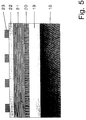
- Fig. 5 is the layer structure of a thin-film solar cell that with that described Process is reproduced.
- the thin nucleation layer (20) which is preferably 4 ⁇ m thick, becomes p-conductive and is highly endowed.
- the photovoltaically sensitive epitaxial layer (21) (layer thickness 5 ⁇ m to 400 ⁇ m, preferably 10 - 30 ⁇ m) deposited.
- the n-layer (22) and the front contact (23) are located above it.
- an MIS inversion-layer solar cell can also be produced on the epitaxial layer (21) become.
Landscapes
- Photovoltaic Devices (AREA)
- Recrystallisation Techniques (AREA)
- Mechanical Treatment Of Semiconductor (AREA)
- Internal Circuitry In Semiconductor Integrated Circuit Devices (AREA)
- Solid State Image Pick-Up Elements (AREA)
Description
- Fig. 1
- eine Prinzipdarstellung einer Anordnung zur Herstellung eines Halbleiter-Bauelements,
- Fig. 2
- eine alternative Ausführungsform einer Anordnung zur Herstellung eines Halbleiter-Bauelements,
- Fig. 3
- Ausbildung von Wärmequellen zum Aufschmelzen einer Keimbildungsschicht,
- Fig. 4
- eine Prinzipdarstellung zur Erläuterung eines Rekristallisationsvorgangs,
- Fig. 5
- einen Aufbau eines Halbleiter-Bauelementes,
- Fig. 6
- ein Schliffbild eines eine Keimbildungsschicht und eine Halbleiterschicht umfassenden Schichtaufbaus und
- Fig. 7
- eine Textur einer Epitaxieschicht eines Halbleiter-Bauelements.
Claims (8)
- Verfahren zur Herstellung eines Halbleiter-Bauelementes, insbesondere Dünnschicht-Halbieiter-Bauelementes wie Dünnschicht-Solarzelle, umfassend einen Träger (1, 12, 18), erste und zweite elektrisch leitende Front- bzw. Rückkontakt (19, 23) bildende Kontakte sowie zumindest eine zwischen diesen vorhandene Halbleiterschicht (21, 22) und eine zwischen der Halbleiterschicht und dem Träger angeordnete Keimbildungsschicht (6, 9, 14, 20), die nach dem Auftragen zunächst lateral kristallisiert wird, um anschließend die Halbleiterschicht epitaktisch auf die Keimbildungsschicht abzuscheiden,
dadurch gekennzeichnet,
dass auf den aus Graphit bestehenden oder Graphit enthaltenden Träger (1, 18) eine diesen versiegelnde Zwischenschicht (19) aus polykristallinem und/oder amorphem SiC aufgetragen wird, die ein Eindringen von Material der Keimbildungsschicht verhindert und die gegenüber der Keimbildungsschicht (6, 9, 14, 20) bei einer Temperatur oberhalb deren Schmelzpunkt thermisch und chemisch stabil ist. - Verfahren nach Anspruch 1,
dadurch gekennzeichnet,
daß die Keimbildungsschicht (6, 9, 14, 20) einer derartigen lateralen Kristallisation mit einem in Richtung des Trägers (1, 12, 18) geneigten Temperaturgradienten unterzogen wird, daß sich in einer parallel zum Träger (1, 12, 18) verlaufenden Ebene eine konvex verlaufende Erstarrungsfront zwischen kristallisiertem Keimbildungsschichtbereich (11) und geschmolzenem Keimbildungsschichtbereich (10) ausbildet. - Verfahren nach Anspruch 1,
dadurch gekennzeichnet,
daß das Aufschmelzen der Keimbildungschicht (6, 9, 14, 20) in einem flächig vorspringenden Bereich oder einem Eckbereich der Keimbildungsschicht eingeleitet wird und/oder daß ein orientierter Keim in den Träger (1, 12, 18) eingelassen wird, und dieser beim Auftragen und Aufschmelzen der Keimbildungsschicht nur teilweise derart aufgeschmolzen wird, daß ein orientiertes laterales Kristallwachstum der kristallierenden Keimbildungsschicht erfolgt. - Verfahren nach zumindest einem der vorhergehenden Ansprüche,
dadurch gekennzeichnet,
daß die den Träger (1, 12, 18) versiegelnde Zwischenschicht (19) eine kontrolliert vorgegebene Oberflächenrauhigkeit durch z.B. Art der Abscheidung der Zwischenschicht, durch Anätzen dieser und/oder mechanisches Bearbeiten aufweist. - Verfahren nach Anspruch 4,
dadurch gekennzeichnet,
daß die Zwischenschicht (19) vor Auftragen der Keimbildungsschicht (20) in einem Gemisch aus Wasserstoff und zumindest einer flüchtigen Borverbindung wie BBr3, B2H6, vorzugsweise BCl3 getempert wird. - Verfahren nach zumindest einem der vorhergehenden Ansprüche,
dadurch gekennzeichnet,
daß die Keimbildungsschicht (6, 9, 14, 20) derart orientiert wird, daß die anschließend epitaktisch aufgetragene Halbleiterschicht (21) mit texturierter Oberfläche wächst. - Verfahren nach zumindest einem der vorhergehenden Ansprüche,
dadurch gekennzeichnet,
daß die laterale Erstarrung der Keimbildungsschicht (6, 9, 14, 20) derart erfolgt, daß Verunreinigungen des Keimbildungsschichtmaterials an der Grenzfläche zwischen der Keimbildungsschicht und der Zwischenschicht (19) angereichert werden. - Verfahren nach einem der vorhergehenden Ansprüche,
dadurch gekennzeichnet,
dass in der Zwischenschicht (19) als zusätzlichs Material Silizium verwendet wird.
Applications Claiming Priority (2)
| Application Number | Priority Date | Filing Date | Title |
|---|---|---|---|
| DE4133644A DE4133644A1 (de) | 1991-10-11 | 1991-10-11 | Halbleiterbauelement, verfahren zu dessen herstellung sowie hierzu benutzte anordnung |
| DE4133644 | 1991-10-11 |
Publications (3)
| Publication Number | Publication Date |
|---|---|
| EP0536682A2 EP0536682A2 (de) | 1993-04-14 |
| EP0536682A3 EP0536682A3 (en) | 1993-10-27 |
| EP0536682B1 true EP0536682B1 (de) | 2000-07-19 |
Family
ID=6442462
Family Applications (1)
| Application Number | Title | Priority Date | Filing Date |
|---|---|---|---|
| EP92117007A Expired - Lifetime EP0536682B1 (de) | 1991-10-11 | 1992-10-06 | Verfahren zur Herstellung eines Halbleiter-Bauelements |
Country Status (5)
| Country | Link |
|---|---|
| US (1) | US5380372A (de) |
| EP (1) | EP0536682B1 (de) |
| JP (1) | JP3771279B2 (de) |
| AT (1) | ATE194884T1 (de) |
| DE (2) | DE4133644A1 (de) |
Families Citing this family (29)
| Publication number | Priority date | Publication date | Assignee | Title |
|---|---|---|---|---|
| TW355845B (en) * | 1995-03-27 | 1999-04-11 | Semiconductor Energy Lab Co Ltd | Semiconductor device and a method of manufacturing the same |
| US7075002B1 (en) * | 1995-03-27 | 2006-07-11 | Semiconductor Energy Laboratory Company, Ltd. | Thin-film photoelectric conversion device and a method of manufacturing the same |
| US6133119A (en) * | 1996-07-08 | 2000-10-17 | Semiconductor Energy Laboratory Co., Ltd. | Photoelectric conversion device and method manufacturing same |
| PT831077E (pt) * | 1996-09-18 | 2002-04-29 | Tece Technical Ceramics Gmbh & | Substrato ceramico para celulas solares de camada fina de silicio cristalino |
| CA2283334A1 (en) * | 1997-03-04 | 1998-09-11 | Astropower, Inc. | Columnar-grained polycrystalline solar cell substrate and improved method of manufacture |
| JP3830623B2 (ja) * | 1997-07-14 | 2006-10-04 | 株式会社半導体エネルギー研究所 | 結晶性半導体膜の作製方法 |
| JP3295346B2 (ja) | 1997-07-14 | 2002-06-24 | 株式会社半導体エネルギー研究所 | 結晶性珪素膜の作製方法及びそれを用いた薄膜トランジスタ |
| DE10060221A1 (de) * | 2000-12-04 | 2002-06-13 | Cfi Ceramics For Industry Gmbh | Substrat auf Basis von Siliciumnitrid für Halbleiter-Bauelemente |
| US7071307B2 (en) * | 2001-05-04 | 2006-07-04 | Syngenta Participations Ag | Nucleic acids and proteins with thioredoxin reductase activity |
| DE102005019797A1 (de) * | 2005-04-28 | 2006-11-09 | Blitzstrom Gmbh | Verfahren zur Herstellung von Solarzellen Substraten |
| US7824579B2 (en) * | 2005-06-07 | 2010-11-02 | E. I. Du Pont De Nemours And Company | Aluminum thick film composition(s), electrode(s), semiconductor device(s) and methods of making thereof |
| US7771623B2 (en) * | 2005-06-07 | 2010-08-10 | E.I. du Pont de Nemours and Company Dupont (UK) Limited | Aluminum thick film composition(s), electrode(s), semiconductor device(s) and methods of making thereof |
| US7718092B2 (en) * | 2005-10-11 | 2010-05-18 | E.I. Du Pont De Nemours And Company | Aluminum thick film composition(s), electrode(s), semiconductor device(s) and methods of making thereof |
| WO2008039461A2 (en) * | 2006-09-27 | 2008-04-03 | Thinsilicon Corp. | Back contact device for photovoltaic cells and method of manufacturing a back contact |
| WO2008150769A2 (en) * | 2007-05-31 | 2008-12-11 | Thinsilicon Corporation | Photovoltaic device and method of manufacturing photovoltaic devices |
| US20100310860A1 (en) * | 2008-02-28 | 2010-12-09 | Changwon National University Industry Academy Cooperation Corps | Synthetic method for anti-oxidation ceramic coatings on graphite substrates |
| US20090250108A1 (en) * | 2008-04-02 | 2009-10-08 | Applied Materials, Inc. | Silicon carbide for crystalline silicon solar cell surface passivation |
| US20090255576A1 (en) * | 2008-04-04 | 2009-10-15 | Michael Tischler | Window solar cell |
| EP2356696A4 (de) * | 2009-05-06 | 2013-05-15 | Thinsilicon Corp | Photovoltaikzellen und verfahren zur verstärkung der lichterfassung in halbleiterschichtstapeln |
| US8398768B2 (en) * | 2009-05-14 | 2013-03-19 | Corning Incorporated | Methods of making an article of semiconducting material on a mold comprising semiconducting material |
| US8540920B2 (en) * | 2009-05-14 | 2013-09-24 | Corning Incorporated | Methods of making an article of semiconducting material on a mold comprising particles of a semiconducting material |
| US20110114156A1 (en) * | 2009-06-10 | 2011-05-19 | Thinsilicon Corporation | Photovoltaic modules having a built-in bypass diode and methods for manufacturing photovoltaic modules having a built-in bypass diode |
| JP2012523716A (ja) * | 2009-06-10 | 2012-10-04 | シンシリコン・コーポレーション | 光起電モジュール、及び、複数半導体層スタックを有する光起電モジュールの製造方法 |
| US20110048530A1 (en) * | 2009-08-31 | 2011-03-03 | Sasha Marjanovic | Surface nucleated glasses for photovoltaic devices |
| US20110086235A1 (en) * | 2009-10-08 | 2011-04-14 | Stewart Engineers, Inc. | Methods of nucleation control in film deposition |
| US8591795B2 (en) * | 2009-12-04 | 2013-11-26 | Corning Incorporated | Method of exocasting an article of semiconducting material |
| US9012253B2 (en) * | 2009-12-16 | 2015-04-21 | Micron Technology, Inc. | Gallium nitride wafer substrate for solid state lighting devices, and associated systems and methods |
| JP4775869B1 (ja) * | 2010-05-27 | 2011-09-21 | シャープ株式会社 | 光電変換装置 |
| CN108028267A (zh) | 2015-08-20 | 2018-05-11 | 恩特格里斯公司 | 碳化硅/石墨复合物与包括所述复合物的物件及组合件 |
Family Cites Families (3)
| Publication number | Priority date | Publication date | Assignee | Title |
|---|---|---|---|---|
| US3961997A (en) * | 1975-05-12 | 1976-06-08 | The United States Of America As Represented By The Administrator Of The National Aeronautics And Space Administration | Fabrication of polycrystalline solar cells on low-cost substrates |
| US4137355A (en) * | 1976-12-09 | 1979-01-30 | Honeywell Inc. | Ceramic coated with molten silicon |
| US4313254A (en) * | 1979-10-30 | 1982-02-02 | The Johns Hopkins University | Thin-film silicon solar cell with metal boride bottom electrode |
-
1991
- 1991-10-11 DE DE4133644A patent/DE4133644A1/de active Granted
-
1992
- 1992-10-06 AT AT92117007T patent/ATE194884T1/de not_active IP Right Cessation
- 1992-10-06 DE DE59209850T patent/DE59209850D1/de not_active Expired - Lifetime
- 1992-10-06 EP EP92117007A patent/EP0536682B1/de not_active Expired - Lifetime
- 1992-10-08 US US07/958,090 patent/US5380372A/en not_active Expired - Lifetime
- 1992-10-12 JP JP27326592A patent/JP3771279B2/ja not_active Expired - Lifetime
Also Published As
| Publication number | Publication date |
|---|---|
| EP0536682A3 (en) | 1993-10-27 |
| DE4133644A1 (de) | 1993-04-15 |
| DE59209850D1 (de) | 2000-08-24 |
| ATE194884T1 (de) | 2000-08-15 |
| US5380372A (en) | 1995-01-10 |
| DE4133644C2 (de) | 1993-07-22 |
| EP0536682A2 (de) | 1993-04-14 |
| JPH05299347A (ja) | 1993-11-12 |
| JP3771279B2 (ja) | 2006-04-26 |
Similar Documents
| Publication | Publication Date | Title |
|---|---|---|
| DE4133644C2 (de) | ||
| DE4138121C2 (de) | Verfahren zur Herstellung einer Solarzelle | |
| Lange et al. | Ribbon Growth on Substrate (RGS)—A new approach to high speed growth of silicon ribbons for photovoltaics | |
| US4159354A (en) | Method for making thin film III-V compound semiconductors for solar cells involving the use of a molten intermediate layer | |
| US4947219A (en) | Particulate semiconductor devices and methods | |
| DE4207411A1 (de) | Duennschicht-solarzelle und verfahren zu deren herstellung | |
| DE2702860A1 (de) | Solarzelle und verfahren zu ihrer herstellung | |
| DE3426338C2 (de) | ||
| DE69411861T2 (de) | Photoelektrische Wandlervorrichtung aus polykrystallinem Silicon und Verfahren zur Herstellung | |
| DE2818261A1 (de) | Halbleiter-solarzelle und verfahren zu ihrer herstellung | |
| EP0541033A2 (de) | Verfahren zur Herstellung von polykristallinen Silizium-Dünnschicht-Solarzellen | |
| DE202025103023U1 (de) | Metall-Halbleiter-Kontaktstruktur, Solarzelle und Photovoltaikmodul | |
| DE19927604A1 (de) | Silicium mit strukturierter Sauerstoffdotierung, dessen Herstellung und Verwendung | |
| JP2005159312A (ja) | 太陽電池用多結晶シリコン基板の母材および太陽電池用多結晶シリコン基板 | |
| Ishihara et al. | High efficiency thin film silicon solar cells prepared by zone‐melting recrystallization | |
| DE10005484B4 (de) | Verfahren zum Ausbilden einer dünnen kristallisierten Schicht | |
| DE19810019A1 (de) | Gerichtet erstarrtes multikristallines Silicium, ein Verfahren zu dessen Herstellung und dessen Verwendung sowie Solarzellen, enthaltend dieses Silicium und ein Verfahren zu deren Herstellung | |
| DE3856275T2 (de) | Kristalline Gegenstände und Verfahren zu ihrer Herstellung | |
| Akani et al. | Diffusion length measurements on plasma-sprayed polycrystalline silicon substrates and on silicon grown on them by chemical vapour deposition | |
| Tsuo et al. | Grain boundary structures and properties in polycrystalline silicon | |
| Reindl et al. | Electrical and structural properties of the Si/C interface in poly-Si thin films on graphite substrates | |
| JP2008053407A (ja) | 多結晶半導体太陽電池及びその製造方法 | |
| DE4229702A1 (de) | Verfahren zur Herstellung von Silizium- und Eisensilizid-Dünnschicht-Solarzellen durch Elektronenstahlrekristallisation | |
| Sopori et al. | Grain enhancement of thin silicon layers using optical processing | |
| Shi et al. | Solution growth of polycrystalline silicon on glass at low temperatures |
Legal Events
| Date | Code | Title | Description |
|---|---|---|---|
| PUAI | Public reference made under article 153(3) epc to a published international application that has entered the european phase |
Free format text: ORIGINAL CODE: 0009012 |
|
| AK | Designated contracting states |
Kind code of ref document: A2 Designated state(s): AT BE CH DE DK ES FR GB GR IT LI LU MC NL PT SE |
|
| PUAL | Search report despatched |
Free format text: ORIGINAL CODE: 0009013 |
|
| AK | Designated contracting states |
Kind code of ref document: A3 Designated state(s): AT BE CH DE DK ES FR GB GR IT LI LU MC NL PT SE |
|
| 17P | Request for examination filed |
Effective date: 19940426 |
|
| RBV | Designated contracting states (corrected) |
Designated state(s): AT BE CH DE FR GB IT LI |
|
| 17Q | First examination report despatched |
Effective date: 19950324 |
|
| GRAG | Despatch of communication of intention to grant |
Free format text: ORIGINAL CODE: EPIDOS AGRA |
|
| RTI1 | Title (correction) |
Free format text: PROCESS OF MANUFACTURING A SEMICONDUCTOR DEVICE |
|
| GRAG | Despatch of communication of intention to grant |
Free format text: ORIGINAL CODE: EPIDOS AGRA |
|
| GRAG | Despatch of communication of intention to grant |
Free format text: ORIGINAL CODE: EPIDOS AGRA |
|
| GRAH | Despatch of communication of intention to grant a patent |
Free format text: ORIGINAL CODE: EPIDOS IGRA |
|
| GRAH | Despatch of communication of intention to grant a patent |
Free format text: ORIGINAL CODE: EPIDOS IGRA |
|
| RAP1 | Party data changed (applicant data changed or rights of an application transferred) |
Owner name: ANGEWANDTE SOLARENERGIE - ASE GMBH |
|
| GRAA | (expected) grant |
Free format text: ORIGINAL CODE: 0009210 |
|
| AK | Designated contracting states |
Kind code of ref document: B1 Designated state(s): AT BE CH DE FR GB IT LI |
|
| REF | Corresponds to: |
Ref document number: 194884 Country of ref document: AT Date of ref document: 20000815 Kind code of ref document: T |
|
| REG | Reference to a national code |
Ref country code: CH Ref legal event code: EP |
|
| REF | Corresponds to: |
Ref document number: 59209850 Country of ref document: DE Date of ref document: 20000824 |
|
| ITF | It: translation for a ep patent filed | ||
| PG25 | Lapsed in a contracting state [announced via postgrant information from national office to epo] |
Ref country code: AT Free format text: LAPSE BECAUSE OF NON-PAYMENT OF DUE FEES Effective date: 20001006 |
|
| ET | Fr: translation filed | ||
| PG25 | Lapsed in a contracting state [announced via postgrant information from national office to epo] |
Ref country code: CH Free format text: LAPSE BECAUSE OF NON-PAYMENT OF DUE FEES Effective date: 20001031 Ref country code: LI Free format text: LAPSE BECAUSE OF NON-PAYMENT OF DUE FEES Effective date: 20001031 Ref country code: BE Free format text: LAPSE BECAUSE OF NON-PAYMENT OF DUE FEES Effective date: 20001031 |
|
| GBT | Gb: translation of ep patent filed (gb section 77(6)(a)/1977) |
Effective date: 20001006 |
|
| BERE | Be: lapsed |
Owner name: ANGEWANDTE SOLARENERGIE - ASE G.M.B.H. Effective date: 20001031 |
|
| PLBE | No opposition filed within time limit |
Free format text: ORIGINAL CODE: 0009261 |
|
| REG | Reference to a national code |
Ref country code: CH Ref legal event code: PL |
|
| 26N | No opposition filed | ||
| REG | Reference to a national code |
Ref country code: GB Ref legal event code: IF02 |
|
| REG | Reference to a national code |
Ref country code: FR Ref legal event code: CD |
|
| REG | Reference to a national code |
Ref country code: FR Ref legal event code: CD |
|
| PGFP | Annual fee paid to national office [announced via postgrant information from national office to epo] |
Ref country code: DE Payment date: 20101022 Year of fee payment: 19 |
|
| PGFP | Annual fee paid to national office [announced via postgrant information from national office to epo] |
Ref country code: IT Payment date: 20101026 Year of fee payment: 19 Ref country code: GB Payment date: 20101021 Year of fee payment: 19 |
|
| PGFP | Annual fee paid to national office [announced via postgrant information from national office to epo] |
Ref country code: FR Payment date: 20111103 Year of fee payment: 20 |
|
| REG | Reference to a national code |
Ref country code: DE Ref legal event code: R071 Ref document number: 59209850 Country of ref document: DE |
|
| REG | Reference to a national code |
Ref country code: DE Ref legal event code: R071 Ref document number: 59209850 Country of ref document: DE |
|
| REG | Reference to a national code |
Ref country code: GB Ref legal event code: PE20 Expiry date: 20121005 |
|
| PG25 | Lapsed in a contracting state [announced via postgrant information from national office to epo] |
Ref country code: GB Free format text: LAPSE BECAUSE OF EXPIRATION OF PROTECTION Effective date: 20121005 |